
 Open Access Article
 This Open Access Article is licensed under a
 Creative Commons Attribution 3.0 Unported Licence
Upper limit to the photovoltaic efficiency of imperfect crystals from first principles†
Sunghyun
Kim
 a,
José A.
Márquez
b,
Thomas
Unold
b and
Aron
Walsh
*ac
a,
José A.
Márquez
b,
Thomas
Unold
b and
Aron
Walsh
*ac
aDepartment of Materials, Imperial College London, Exhibition Road, London SW7 2AZ, UK. E-mail: a.walsh@imperial.ac.uk
bHelmholtz-Zentrum Berlin für Materialien und Energie GmbH, Department Structure and Dynamics of Energy Materials, Hahn-Meitner-Platz 1, D-14109 Berlin, Germany
cDepartment of Materials Science and Engineering, Yonsei University, Seoul 03722, Korea
First published on 9th March 2020
Abstract
The Shockley–Queisser (SQ) limit provides a convenient metric for predicting light-to-electricity conversion efficiency of a solar cell based on the band gap of the light-absorbing layer. In reality, few materials approach this radiative limit. We develop a formalism and computational method to predict the maximum photovoltaic efficiency of imperfect crystals from first principles. The trap-limited conversion efficiency includes equilibrium populations of native defects, their carrier-capture coefficients, and the associated recombination rates. When applied to kesterite solar cells, we reveal an intrinsic limit of 20% for Cu2ZnSnSe4, which falls far below the SQ limit of 32%. The effects of atomic substitution and extrinsic doping are studied, leading to pathways for an enhanced efficiency of 31%. This approach can be applied to support targeted-materials selection for future solar-energy technologies.
Sunlight is the most abundant source of sustainable energy. Similar to the Carnot efficiency of heat engines, the maximum efficiency for photovoltaic energy conversion is determined by thermodynamics and can be as high as 86% owing to the high temperature of the sun.1,2 However, in practical solar cells with single p–n semiconductor junctions, large irreversible energy loss occurs mainly through hot-carrier cooling and low light absorption below the band gap.3
The Shockley–Queisser (SQ) limit describes the theoretical sunlight-to-electricity conversion efficiency of a single-junction solar cell.3 The SQ limit (33.7% under AM1.5g illumination) and its variations, including spectroscopic limited maximum efficiency (SLME),4 determine the maximum efficiency of a solar cell based on the principle of detailed balance between the absorption and emission of light. The amount of photons absorbed determines the short-circuit current density JSC, and, hot-carrier cooling and radiative recombination limit the maximum carrier concentration and hence the open-circuit voltage VOC.
In the SQ limit, the predicted efficiency is a function of the semiconductor band gap, which is a trade-off between light absorption (current generation) and energy loss due to hot-carrier cooling. This analysis secured the band gap as a primary descriptor when searching for new photovoltaic compounds, often within a 1–1.5 eV target window. Unfortunately, few materials approach the SQ limit. Less than 10 classes of materials have achieved conversion efficiency greater than 20%.5 Most emerging technologies struggle to break the 10% efficiency threshold.
Kesterites are a class of quaternary materials studied for thin-film photovoltaic applications. Although a lot of progress has been made during the past few decades, the certified champion efficiency of 12.6%6 has been increased by less than 0.1% since 2013.7 The main bottleneck is the low open-circuit voltage, which is far below the SQ limit.8 Many routes to engineer compositions and architectures have been considered, but it is not clear which process dominates.9 One of the biggest questions in the field is if there is an intrinsic problem with kesterite semiconductors that prevent them approaching the radiative limit.10–12
The discrepancy between the SQ limit and efficiencies of real solar cells results from the extra irreversible processes such as electron–hole nonradiative recombination. While Shockley and Queisser studied the effect of the nonradiative recombination, it has been treated as a parameter of radiative efficiency and often a radiative efficiency of 100% is assumed, which is unrealistic for real materials.
The rate of nonradiative recombination mediated by traps can be described by Shockley–Read–Hall statistics.13,14 The steady-state recombination rate is determined by the detailed balance where the net electron-capture rate is equal to the net hole capture rate. A microscopic theory of carrier capture was proposed by Henry and Lang in 1977.15 The thermal vibration of the defect, together with the electron–phonon coupling, causes charge transfer from a delocalised free carrier to a localised defect state. Thus the carrier capture coefficient heavily depends on the electron and phonon wave functions associated with a defect, which are difficult to probe experimentally. Instead, the microscopic processes in materials, including nonradiative carrier capture, have been inferred from macroscopic responses such as a capacitance transient.15 Macroscopic properties of solar cells (e.g. open-circuit voltage and device efficiency) and microscopic processes in the material (e.g. carrier capture coefficient) are rarely connected. Therefore, although theories of solar cells are well known, the theoretical approaches have failed to provide a priori predictions of photovoltaic efficiencies of real materials.
Each material has a fundamental limit of radiative efficiency because the material contains a certain amount of native defects. Their concentrations in thermal equilibrium are intrinsic properties of the materials, and the resulting ‘soup’ of defects determines the maximum radiative efficiency. Recently, first-principles methods based on density functional theory (DFT) have been developed to calculate the nonradiative carrier capture,16–18 which opens up the possibility for studying the theoretical upper-bound of photovolataic efficiency of a real material limited by both the radiative and the nonradiative recombination.
In this work, we propose a first-principles method of the trap-limited conversion efficiency (TLC) to calculate the upper-limit of photovolatic efficiency of a material containing the number of native defects in thermal equilibrium. To take into account both radiative and nonradiative processes, we perform a series of calculations for kesterites. The absorption and the emission of light are calculated in the framework of Shockley and Queisser. To obtain the nonradiative recombination rate, we calculate the carrier capture coefficients and equilibrium concentrations of native defects. The workflow for our method is shown in Fig. 1. We conclude that kesterite solar cells suffer from significant nonradiative recombination and are unable to reach the SQ limit even under optimal growth conditions. Strategies to overcome such rapid recombination rates are suggested.
 | ||
| Fig. 1 Diagram for the calculation of trap-limited conversion efficiency. The dependent calculations are connected by lines. For each numbered step, the calculated quantities are appended. The red and blue boxes represent calculations for radiative and nonradiative electron–hole recombination, respectively. The combined device simulations are marked in green. The corresponding physical processes are detailed and illustrated in the ESI.† | ||
I. Theory
A. Radiative recombination
The short-circuit current JSC of a solar cell whose absorber thickness is W is given by the absorbed photon flux multiplied by an elementary charge q: | (1) |
The radiative recombination rate for the solar cell at temperature T is given by
 | (2) |
 | (3) |
In the SQ limit, an absorptivity is assumed to be a step function being 1 above the band gap Eg and 0 otherwise, while a real material has a finite absorptivity with a tail near the band gap Eg, which depends on the sample thickness. Rau et al.19 defined a photovoltaic band gap using the absorption edge spectrum and found that, in inorganic solar cells, the effect of the finite absorption tail on the open-circuit voltage loss is small.19
B. Nonradiative recombination
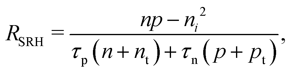
A material in thermal equilibrium will contain a population of native defects. Defect processes are unavoidable and define the upper limit of performance of optoelectronic devices. The nonradiative recombination at charge carriers via defects is often a dominant source of degradation of solar cells and should be carefully controlled.20Based on the principle of detailed balance,13,14 the steady-state recombination rate RSRHvia a defect with electron-capture coefficient Cn and hole-capture cross coefficient Cp is given by
 | (4) |
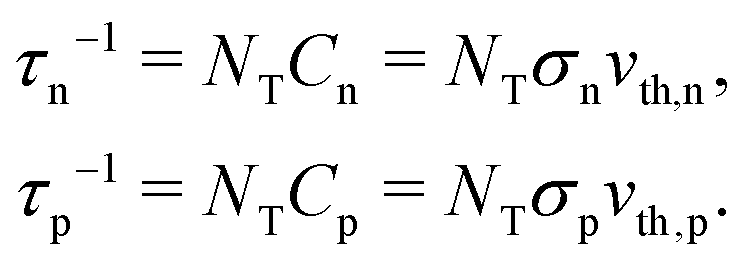 | (5) |
For doped semiconductors, minority carrier lifetime often determines the rate of the total recombination process. For example, in a p-type semiconductor where the acceptor concentration, p0, is much higher than the photoexcited carrier density, the RSRH due to a deep defect is proportional to the (photoexcited) excess carrier density Δn:21
 | (6) |
The calculation of RSRH requires three properties of a defect (concentration NT, defect level ET, and capture coefficient Cn/p) in addition to the carrier concentrations n and p, as well as the intrinsic doping density n0 or p0 in the bulk host, as explained in the following subsections.
Phase diagram. The growth environment of a crystal including elemental ratio, partial pressures, and temperature determines the properties of the material including concentrations of the native defects. In a theoretical framework, the growth conditions can be expressed using the thermodynamic chemical potential μ of each element. We compare the energies of kesterites and their competing secondary phases, showing a range of chemical potentials that favors the formation of kesterites, using CPLAP.27 We can avoid the formation of the secondary phases by a careful choice of synthesis conditions. However even ‘pure’ kesterites without secondary phases will contain native defects whose concentrations are controlled by this choice of chemical potentials.
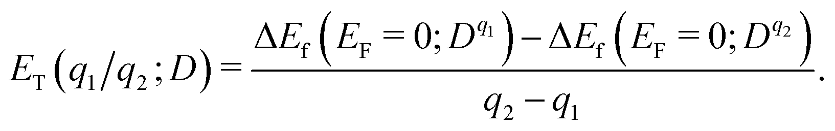
Formation energy of a defect. We calculated the formation energy ΔEf(Dq) of a defect D with the charge state q as given by28
 | (7) |
Self-consistent Fermi level. For a given synthesis condition (set of atomic chemical potentials), the formation energy is a function of the Fermi level as shown in eqn (7), while the Fermi level is determined by the concentrations of charged defects and carriers. Thus we calculate the equilibrium concentrations of defects and carriers, and the Fermi level self-consistently under the constraint of charge neutrality condition for overall system of defects and charge carriers using SC-FERMI.31
For a given Fermi level, the equilibrium concentration of a defect N(Dq) is given by
| N(Dq) = Nsitege−ΔEf(Dq)/kBT, | (8) |
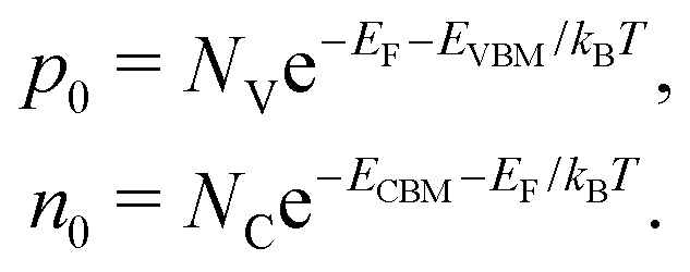
The concentrations of holes p0 and electrons n0 are determined by the effective density of states of valence band NV and conduction band NC:
 | (9) |
The net charge of defects should be compensated by the net charge of electrons and holes:
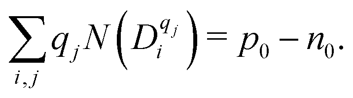 | (10) |
 | (11) |
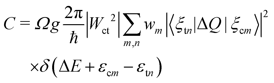
The carrier capture coefficient C can be expressed using the electron–phonon coupling Wct and the overlap of phonon wave functions 〈ξcm|ΔQ|ξtn〉,17,18 which is given by
 | (12) |
 | (13) |
 | (14) |
 . Accordingly, the steady-state concentrations of electron n and hole p under applied voltage V are given by
 | (15) |
C. Trap-limited conversion efficiency
By taking into account the carrier annihilation due to both radiative recombination (eqn (3)) and nonradiative recombination (eqn (4)), the trap-limited current density J under a bias voltage V is given by | (16) |
 | (17) |
II. Results
We apply our scheme to kesterite solar cells (Cu2ZnSnSe4, Cu2ZnSnS4, Cu2ZnGeSe4, and Ag2ZnSnSe4), with details presented in the Methods section and Tables S1 and S2 (ESI†).A. Cu2ZnSnSe4 and Cu2ZnSnS4
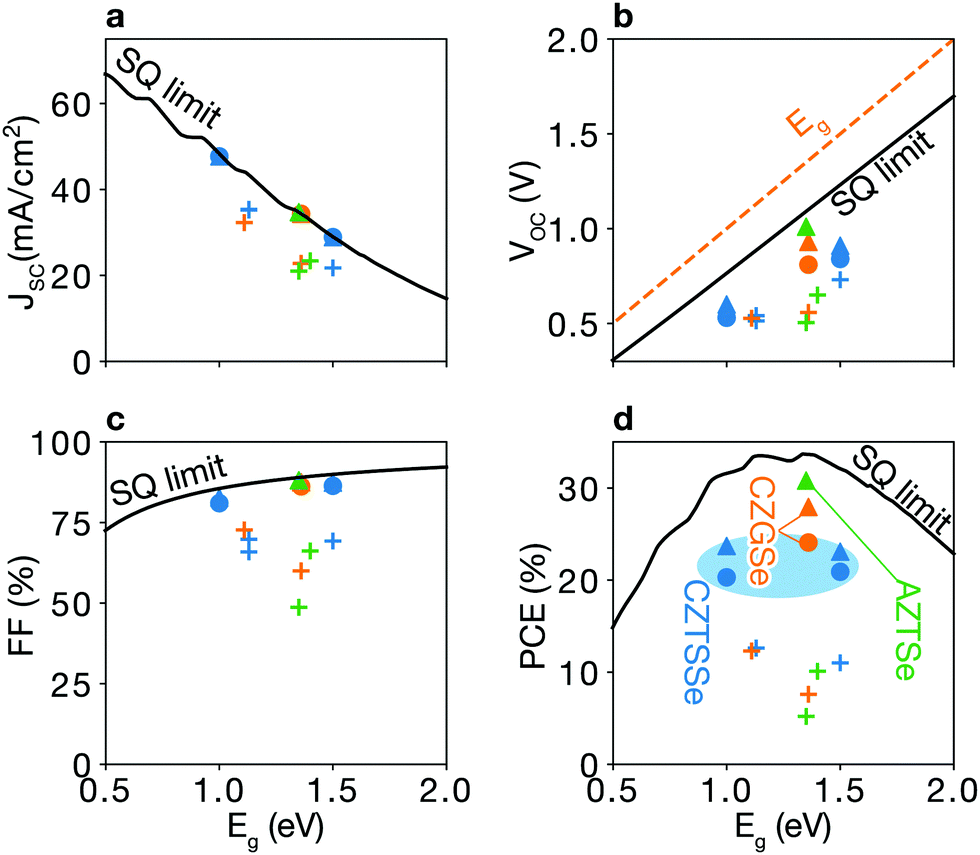 | ||
| Fig. 2 Shockley–Queisser limit and trap-limited-conversion efficiency. (a) Short-circuit current density JSC, (b) open-circuit voltage VOC, (c) fill factor FF, and (d) efficiency η. Filled symbols represent the trap-limited conversion (TLC), while a black line is the SQ limit. TLCs with doping (triangles) show better performances as compared to TLCs without doping (circles). Plus signs indicate experimental data for kesterite solar cells taken from ref. 6, 7 and 22–26. The detailed values are listed in Table 1. | ||
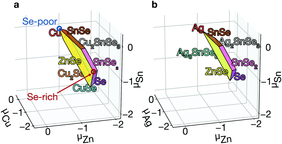 | ||
| Fig. 3 Growth condition. Calculated phase diagrams of Cu2ZnSnSe4 (a) and Ag2ZnSnSe4 (b) where μi = 0 represents the chemical potential of element i in its elemental state. Each plane represents a phase boundary with the secondary phase. Blue and red circles indicate Se-poor and Se-rich conditions, respectively. | ||
The band structure of CZTSe is composed of antibonding Sn 5s–Se 4p* state at the lower conduction band and antibonding Cu 3d–Se 4p* state at the upper valence band. According to models for defect tolerance,35,36 the Cu dangling bond would produce a shallow level, while a deep level can be introduced by the Sn dangling bond. Moreover, the cation antisites, especially (Cu,Zn)Sn and Sn(Cu,Zn) are expected to be deep due to the large difference in the site electrostatic (Madelung) potentials.37
Admittance spectroscopy (AS) measurements identified several shallow acceptors in Cu2ZnSn(S,Se)4, CZTSSe, CZTSe and CZTS at an energy range between 0.05–0.17 eV,38–43 which were attributed to VCu and CuZn. They also found a deep level close to the midgap (ET = 0.5 eV). A series of deep-level transient spectroscopy (DLTS) experiments also revealed the presence of the shallow levels as well as a broad spectrum of deep levels around the mid gap.44–46 Transient photocapacitance (TPC) spectra showed sub-band-gap absorption via deep defects near 0.8 eV with broad bandwidth.47,48 Theoretical calculations37,49–51 revealed the atomic origins of shallow defects: acceptors VCu and CuZn and a donor ZnCu. Several atomic models for the deep defects have been proposed such as (Cu3)Sn, SnZn, VS, VS–CuZn, and SnZn–CuZn.37,49–51
First, we find shallow acceptors (VCu and CuZn) and a shallow donor (ZnCu) (see Fig. 4a and Table S3, ESI†). Due to the similar ionic radii of Cu and Zn, the energy cost for the formation of CuZn and ZnCu is very low. The very low formation energy of CuZn for every set of chemical potentials is largely responsible for the p-type Fermi level around 0.2 eV. We find that the decrease in oxidation state of Sn found in VSe, SnZn and VSe–CuZn produces deep levels, similar to those found in CZTS.37,49–51 The deep donor SnZn becomes shallow when it combines with CuZn because of the Coulomb attraction between the ionized donor and acceptor.50
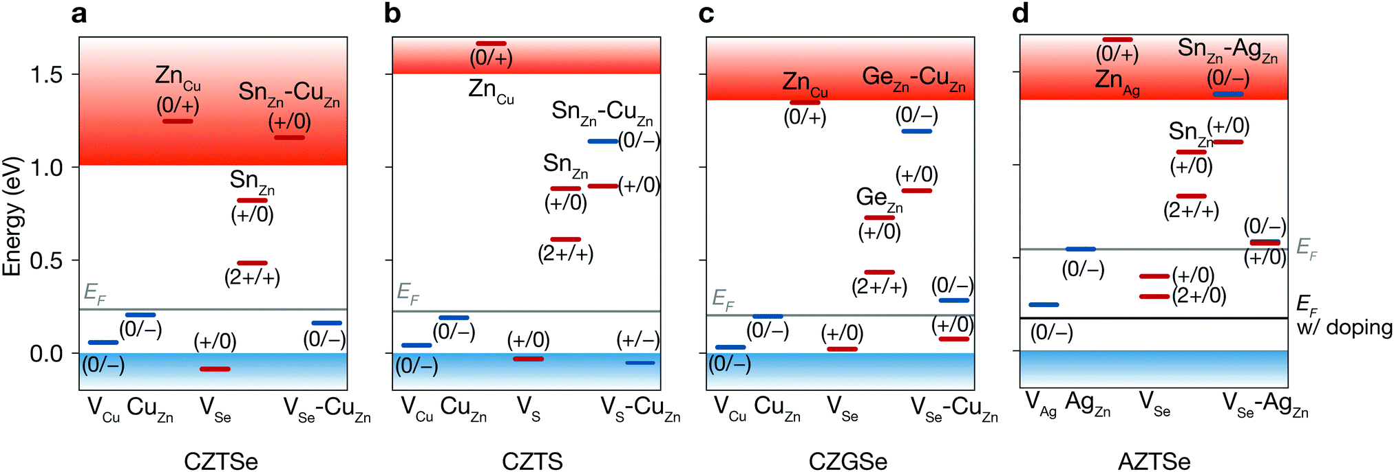 | ||
| Fig. 4 Defect levels of native defects. Donor (red) and acceptor (blue) levels of native point defects of Cu2ZnSnSe4 (a), Cu2ZnSnS4 (b), Cu2ZnGeSe4 (c), and Ag2ZnSnSe4 (d). Blue and red bands represents valence and conduction bands, respectively. Fermi levels are shown in gray lines. The black line in d represents the Fermi level of Ag2ZnSnSe4 with a doping density of 1020 cm−3. | ||
Due to the Sn reduction associated with these defects, they exhibit not only a deep level, but also a large structural relaxation that leads to large electron-capture coefficients.37,50Fig. 5a shows the configuration coordinate for SnZn(2+/1+), illustrating that the carrier-capture barrier is small due to the large lattice relaxation, the horizontal shift of the potential energy surface of Sn1+Zn with respect to that of Sn2+Zn. Thus, we find that SnZn(2+/1+) has a large electron-capture coefficient of 9 × 10⁻⁷ cm3 s−1 (corresponding to the capture cross section of 9.29 × 10⁻¹⁴ cm3 s−1), which classify them as killer centers.52 Note that the minority-carrier capture coefficient of these native defects in CZTSe are of a similar order of magnitude of the most detrimental extrinsic impurities in Si solar cells.53,54 We also find a large electron-capture coefficient of VSe–CuZn, which is listed in Table S3 (ESI†).
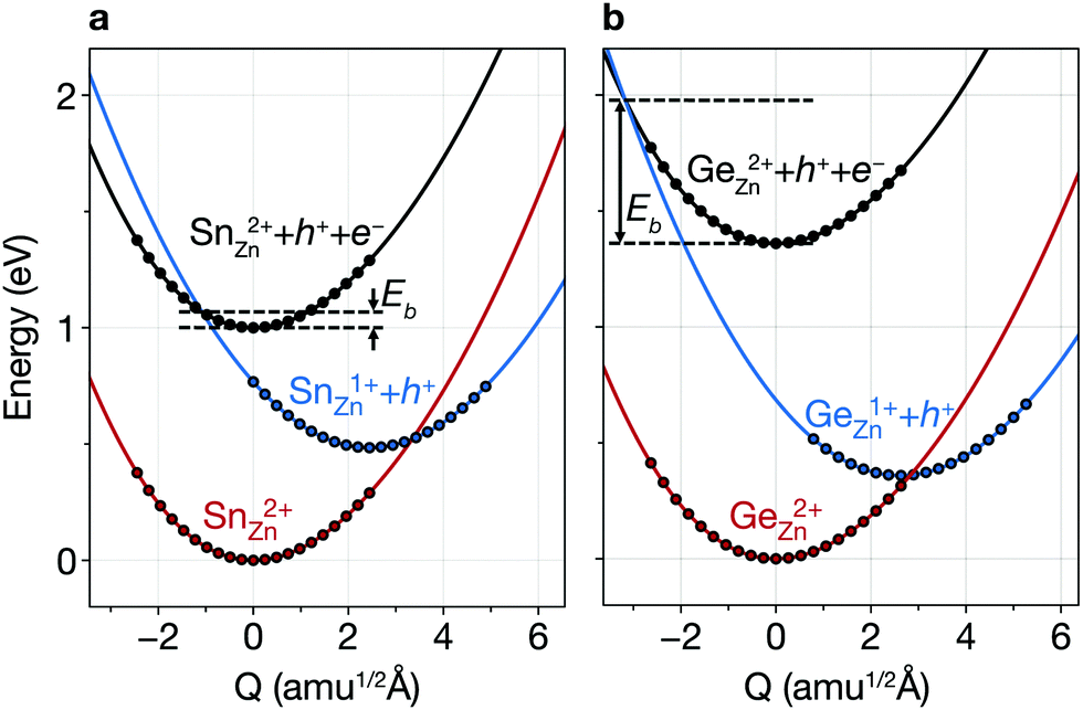 | ||
| Fig. 5 Configuration coordinate diagram for carrier capture. Potential energy surfaces for the vibrations of SnZn (2+/+) in Cu2ZnSnSe4 (a) and GeZn (2+/+) in Cu2ZnGeSe4 (b). The solid circle represents the relative formation energy calculated using DFT, and the line is a spline fit. Eb represents the electron-capture barrier. | ||
Equilibrium concentration. The concentration of native point defects can be tuned through the chemical environment. However, we find that it is difficult to reduce the concentration of the killer centers in CZTSe. For example, to reduce the concentration of SnZn, we need: (i) to increase Zn incorporation, (ii) to decrease Sn incorporation, or (iii) to decrease hole concentration. These are difficult to achieve due to the narrow thermal equilibrium phase diagram. First, the high-Zn incorporation is difficult to achieve because of the aforementioned high stability of ZnSe. On the other hand, the incorporation can be tuned to decrease the concentration of SnZn. The low Sn incorporation, together with the low Zn incorporation, will, however, result in the formation of the highly conductive secondary phases of CuSe and Cu2Se (see Fig. 3a), which can electrically short the device.55 Thus, the low Sn incorporation should actually be avoided. We also find the hole concentrations are high under all conditions due to the high concentrations of CuZn, which is also the consequence of the poor Zn incorporation. Therefore, it is difficult to decrease the concentrations of SnZn in thermal equilibrium.
Fig. 6a shows the equilibrium concentrations of native defects under Se-poor and Se-rich conditions (see Fig. 3a). Under Se-poor conditions, we find high concentration of VSe–CuZn, which is an efficient recombination center. While their concentrations can be significantly decreased through Se incorporation, the concentration of SnZn can not be decreased below 1014 cm−3, which limits the maximum performance of CZTSe solar cells.
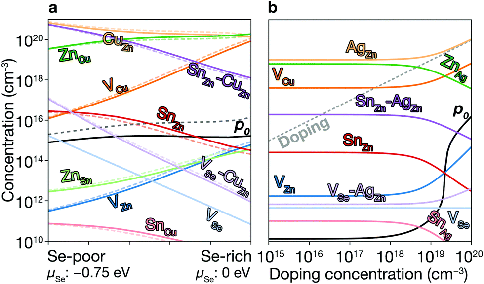 | ||
| Fig. 6 Concentrations of native defects. (a) The concentrations of native defects in CZTSe. The dashed lines represent the concentration with the doping during the growth (see text for details). (b) The concentrations of native defects in AZTSe with the doping during the growth. The dashed diagonal line represents the doping concentration. | ||
Finally, we stress that the capture cross section and defect concentrations of the dominant recombination center in CZTSe (SnZn) are in good agreement with experiments.40,56 Our previous admittance spectroscopy40 revealed a deep defect level located at 0.5 eV. Based on the thermal emission prefactors of up to 5 × 1012 cm s−1 at room temperature, we estimate the capture cross section as 1 × 10⁻¹³ cm2 which agrees well with our calculation of 9 × 10⁻¹⁴ cm2 (see Table S3, ESI†). We also find the longest minority-carrier lifetime achievable is less than 5.5 ns in CZTSe which closely agrees with the previous assessment of the real minority-carrier lifetime of below 1 ns based on time-resolved photoluminescence.56,57
Trap-limited conversion efficiency. We calculate the current–voltage characteristic (eqn (16)) of a CZTSe solar cell containing the equilibrium concentrations of native point defects under the Se-rich condition (see Fig. 7a). We used the a film thickness of 2 μm. The overall power-conversion efficiency is 20.3%, which is below two thirds of the SQ limit of 31.6% (see Fig. 2 and Table 1).
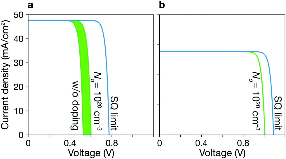 | ||
| Fig. 7 Current–voltage simulation. J–V curves for CZTSe (a) and AZTSe (b) solar cells based on the properties of the bulk absorber materials and not including interfacial processes. Green lines represent the TLCs with various doping concentrations up to 1020 cm−3. The SQ limit is shown in the blue curve. | ||
| E gap (eV) | η (%) | J SC (mA cm−2) | V OC (V) | FF (%) | Ref. | |
|---|---|---|---|---|---|---|
| CZTS | 1.50 | 32.1 | 28.9 | 1.23 | 90.0 | SQ limit |
| CZTSe | 1.00 | 31.6 | 47.7 | 0.77 | 85.7 | SQ limit |
| CZGSe | 1.36 | 33.3 | 34.3 | 1.10 | 89.1 | SQ limit |
| AZTSe | 1.35 | 33.7 | 34.7 | 1.09 | 89.0 | SQ limit |
| CZTS | 1.50 | 20.9 | 28.9 | 0.84 | 86.4 | TLC |
| CZTSe | 1.00 | 20.3 | 47.7 | 0.53 | 81.0 | TLC |
| CZGSe | 1.36 | 24.1 | 34.3 | 0.81 | 86.2 | TLC |
| CZTS:H | 1.50 | 23.1 | 28.9 | 0.91 | 87.4 | TLC |
| CZTSe:H | 1.00 | 23.7 | 47.7 | 0.60 | 82.7 | TLC |
| CZGSe:H | 1.36 | 27.9 | 34.3 | 0.93 | 87.5 | TLC |
| AZTSe:H | 1.35 | 30.8 | 34.7 | 1.01 | 88.1 | TLC |
| CZTS | 1.50 | 11.0 | 21.7 | 0.73 | 69.27 | Exp.25 |
| CZTSe | 1.00 | 11.6 | 40.6 | 0.42 | 67.3 | Exp.70 |
| CZTSSe | 1.13 | 12.6 | 35.4 | 0.54 | 65.9 | Exp.6 |
| CZTGSe | 1.11 | 12.3 | 32.3 | 0.53 | 72.7 | Exp.22 |
| CZGSe | 1.36 | 7.6 | 22.8 | 0.56 | 60 | Exp.26 |
| AZTSe | 1.35 | 5.2 | 21.0 | 0.50 | 48.7 | Exp.23 |
| ACZCTS | 1.40 | 10.1 | 23.4 | 0.65 | 66.2 | Exp.24 |
Sulfide kesterite. Cu2ZnSnS4 (CZTS) also suffers from nonradiative recombination due to the redox activity of Sn and the narrow phase space limited by the high stability of ZnS. Similar to SnZn in CZTSe, we find the large structural relaxation for SnZn that causes fast carrier capture. Moreover, although the defect complex SnZn–CuZn is a shallow donor in CZTSe, in CZTS having the larger band gap of 1.5 eV, SnZn–CuZn produces the deep donor level at ET = 0.90 eV as shown in Fig. 4a and b. Thus, the recombination pathways in CZTS are not only through the isolated SnZn but also the SnZn bound to the acceptor CuZn, which agrees well with a previous theoretical study.51 We find that the similar behavior for GeZn in Cu2ZnGeSe4 which will be discussed in detail in the following section. We calculate a nonradiative VOC loss of 0.39 V, corresponding to an achievable VOC of 0.84 V and a maximum TLC of 20.9% for CZTS, which is similar to that of CZTSe.
B. Cu2ZnGeSe4
As the redox activity of Sn is one culprit that reduces the voltage and efficiency of CZTSe and CZTS devices, we can suppress the nonradiative recombination by substituting Sn with other cations such as Si with a more stable 4+ oxidation state. However, the SQ limit of Cu2ZnSiSe4 is below 16% because of its large band gap of 2.33 eV.58 On the other hand, Cu2ZnGeSe4 (CZGSe) has an optimal band gap of 1.36 eV with an SQ limit of 33.6%. However, we find that the similar redox activity of Ge in CZGSe causes significant nonradiative recombination and limits the VOC.Ge also exhibits an inert-pair effect with large ionisation energy for the 4s orbital. Thus, Ge-related defects (GeZn, GeZn–CuZn, VSe and VSe–CuZn) introduce deep donor levels in the band gap. GeZn exhibits the similar potential energy surfaces to those of SnZn in CZTSe (Fig. 5b). However, GeZn has a deeper donor level than that of SnZn due to the larger band gap of CZGSe (see Table S2, ESI†). As shown in Fig. 5, because the electron-capture processes due to SnZn and GeZn are in the so-called “Marcus inverted region”,59 the deeper donor level of GeZn results in a higher energy barrier for electron-capture (0.62 eV). We find a several orders of magnitude smaller electron-capture coefficient for GeZn (2+/1+) as compared to that of SnZn (2+/1+), implying that the recombination due to the isolated GeZn is unlikely to happen (see Table S3, ESI†).
However, the nonradiative recombination rate in CZGSe is still high due to defect complexation. The abundant acceptor CuZn tends to form a defect complex with donors such as GeZn. The Coulomb attraction between the ionized donor and acceptor further promote the formation of the complex. Moreover, the donor–acceptor complex makes the defect level shallower (ET = 0.87 eV).50 We find that the electron-capture barrier is 71 meV for GeZn–CuZn (1+/0), which is the dominant recombination pathway in CZGSe. Although, we considered only the GeZn and CuZn pair bound at the closest site, in reality, there are a variety of complexes with a wide range of distances between SnZn and CuZn. Such a spectrum of complexes are partially responsible for the broad defect levels in kesterites measured in photocapacitance spectroscopies.47,48
By taking into account the formation of defect complexes, we find significant nonradiative loss in CZGSe. The maximum efficiency is predicted to be 24.1% with large non-radiative open-circuit voltage loss of 0.29 V (see Fig. 2 and Table 1).
C. Hydrogen and alkali-metal doping, and Ag2ZnSnSe4
As an additional lever to tune the defect profiles, we consider extrinsic doping. The formation energy, and hence concentration, of a defect depends on the chemical potential of an electron (Fermi level). In CZTSe, CZTS, and CZGSe, the intrinsic Fermi levels are pinned ∼0.2 eV above the valence band (Fig. 4a–c), promoting the formation of deep donors. As illustrated in Fig. 8a, such high concentrations of donors arise at high (growth) temperature and remain after cooling because they are mostly immobile vacancies and antisites. While n-type doping can increase the Fermi level, this type of doping will not increase the VOC (efficiency) for a material with limited minority carrier lifetime, because n-type doping will decrease the p-type conductivity.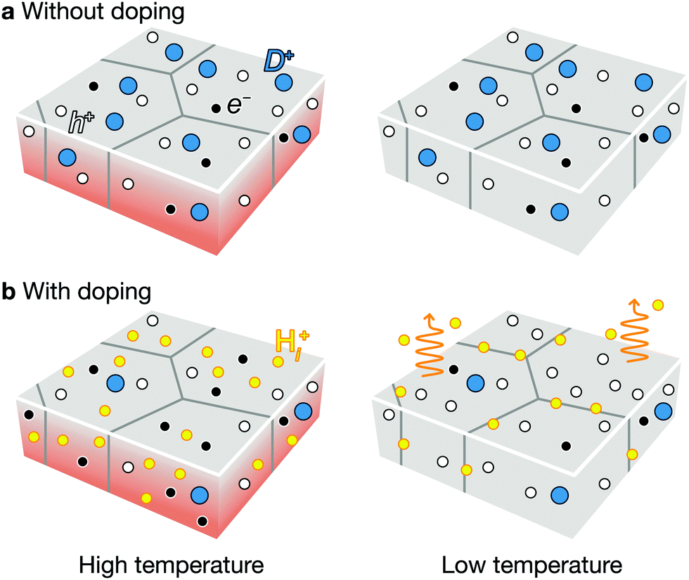 | ||
| Fig. 8 The effect of hydrogen/alkali-metal doping on kesterites. Schematics for the formation of defects without doping (a) and with doping (b). During thermal annealing, the native defects are formed at high temperature (left panel), whose populations remain the same when the sample is cooled down to low temperature (right panel). A high concentration of hole (white circle) promote the formation of donors (blue circle). Dopants are marked as yellow circles. For the clarity, the acceptors are not drawn. | ||
Instead, we predict that hydrogen and alkali-metal doping is helpful to increase the efficiency. At high temperature during the thin-film growth or thermal annealing, the incorporation of the hydrogen or alkali metals at the interstitial sites will increase the Fermi level as they act as donors in p-type semiconductors.60 The high Fermi level decreases the hole concentration and the formation of donor type defects as well (see Fig. 8c). Since hydrogen and alkali-metals are mobile, they tend to diffuse easily and segregate to the grain boundary or outgas, when the thin-film cools down to the room temperature (see Fig. 8d). The final thin-film will exhibit an increased hole concentration and longer carrier lifetime, consistent with the experiments.61 This is indeed the mechanism behind the success of hydrogen-codoping in nitride semiconductors.62,63
We calculate the concentrations of defects in CZTSe with a n-type doping concentration of 1020 cm−3 at T = Tan. Once the dopants are removed, the hole concentration increases by an order of magnitude at T = Top, and the concentration of SnZn is significantly lowered (see Fig. 6a). Thus, the maximum efficiency increases up to 23.7% (Fig. 2 and 7a). This requires a high level of doping to gain a noticeable improvement due to the high concentration of native donors and acceptors, and the self-compensation mechanism via them. Alkali-metal elements may be less effective dopants due to their low solubility.61 On the other hand, the previous calculations60 have shown that the formation energies of Hi in kesterites are low at p-type Fermi-level, suggesting high solubility of H in kesterites. We also noted that Son et al. formed a S–Se grading in the current champion device6 using H2S gas, which may introduce the H-doping unintentionally and be responsible for the high efficiency.
The low formation energies and the high concentrations of CuZn and ZnCu originate from the similar ionic radii of Cu1+ and Zn2+. We may decrease their concentrations by exploiting Ag substituting Cu or Cd substituting Zn.64 Ag substitution for Cu gives Ag2ZnSnSe4 (AZTSe), which also has a narrow phase diagram as shown in Fig. 3b. However, we find several orders of magnitude lower concentrations of the dominant acceptor and donor, AgZn and ZnAg (see Fig. 6b). AZTSe is an intrinsic semiconductor under Se-rich conditions, while n-type Fermi level was found under Se-poor conditions.
For a set of atomic chemical potentials determined under Se-rich conditions, the calculated self-consistent Fermi-level is 0.55 eV above the valence band. Due to the low hole concentration in AZTSe, eqn (6) is not valid, and the hole-capture process becomes the bottleneck in the recombination process owing to the high hole-capture barrier of 0.20 eV as compared to the electron-capture barrier of 0.11 eV. However, due to the high Fermi level in AZTSe or even n-type conductivity, Ag-based solar cells based on the commonly used thin-film architecture for Cu-based kesterites (Mo/kesterite/CdS/ZnO/ITO), have been found to exhibit limited device performance.23,65,66 Notwithstanding these practical challenges, we predict that Ag-based kesterites should show much lower non-radiative recombination and thus possess a significantly larger efficiency potential than the previously discussed Cu- or Ge-based kesterites. Indeed, increased photoluminescence quantum yields (PLQY) have been recently observed for Ag-substituted kesterites.67
An extrinsic n-type doping level of 1020 cm−3 during growth can lower the room temperature Fermi-level to 0.18 eV. As shown in Fig. 6b, this causes the concentration of SnZn to decrease below 1014 cm−3, enhancing the maximum efficiency up to 30.8% (see Fig. 2 and 7), implying that co-doped AZTSe is a promising material as a p-type absorber if the synthesis and processing be appropriately controlled.
D. Calculation of optoelectronic parameters
The achievable solar cell parameters estimated for four types of kesterite materials using our first-principles approach are summarized in Table 1, and compared with the (defect-free) Shockley–Queisser limit, as well as current champion devices.The Ge- and Ag-based materials so far significantly underperform, and that big leaps in efficiency appear possible by the proposed co-doping strategy. Device performance can be limited by a number of non-idealities such as non-optimised functional layers, wrong band line-ups, as well as interface recombination. It is therefore helpful to consider the main (absorber layer) optoelectronic parameters that are experimentally accessible even without building devices. Among the most relevant to judge potential device performance are carrier lifetime, net doping density, and external PLQY, which indicates the ratio of radiative recombination over the total recombination, typically dominated by non-radiative processes. The PLQY can be estimated from non-radiative voltage loss using ΔVnonradOC = kBT![[thin space (1/6-em)]](https://www.rsc.org/images/entities/char_2009.gif) ln(PLQY).68
ln(PLQY).68
A summary of these parameters, calculated from first-principles, are listed in Table 2, indicating small PLQY and lifetimes for CZTS and large PLQY and long lifetimes for co-doped AZTSe. The small predicted PLQY for CZTS is in agreement with observations that the luminescence yield of this material is consistently below the detection limit (ca. 1 × 10⁻⁴%). Also, the PLQY value of 1 × 10⁻²% is consistent with recent reports of 1.5 × 10⁻³% measured on a CZTSe single crystal57 and of 3 × 10⁻³% on 11.6% efficient Li-doped CZTSSe solar cells.69
| E gap (eV) | ΔVnonradOC (V) | p 0 (cm−3) | τ SRH (ns) | PLQY (%) | |
|---|---|---|---|---|---|
| CZTS | 1.50 | 0.39 | 3.3 × 10¹⁵ | 0.13 | 3.1 × 10⁻⁵ |
| CZTSe | 1.00 | 0.24 | 1.7 × 10¹⁵ | 3.4 | 9.8 × 10⁻³ |
| CZGSe | 1.36 | 0.29 | 9.0 × 10¹⁵ | 0.21 | 1.4 × 10⁻³ |
| AZTSe | 1.35 | 1.0 × 10¹⁰ | |||
| CZTS:H | 1.50 | 0.32 | 3.8 × 10¹⁶ | 0.21 | 4.5 × 10⁻⁴ |
| CZTSe:H | 1.00 | 0.17 | 1.8 × 10¹⁶ | 5.5 | 1.5 × 10⁻¹ |
| CZGSe:H | 1.36 | 0.17 | 4.8 × 10¹⁷ | 0.38 | 1.5 × 10⁻¹ |
| AZTSe:H | 1.35 | 0.08 | 1.7 × 10¹⁶ | 1130 | 4.6 |
In these solar cells the lifetime did not change significantly with Li-doping, while the PLQY and net doping density increased, again inline with our predictions. With regards to the calculated minority carrier lifetimes, we point out that the small estimated lifetimes for CZTS and CZTSe are in good agreement with recent findings indicating that reported carrier lifetimes for kesterites are often overestimated and that (typical) real lifetimes are in fact below 1 ns.56
III. Conclusions
We have combined the physics of solar cells with modern first-principles defect theory to assess the efficiency limit of solar cells. We have included the thermal equilibrium concentrations of native defects of the absorber material, which reduces carrier lifetime, and have proposed a first-principles method to calculate the maximum efficiency limited by recombination centers. Sn-Based kesterites suffer from severe nonradiative recombination due to native point defects. The fast nonradiative recombination can be mitigated by extrinsic doping and Ag-alloying, reducing the concentration of recombination centres, thereby increasing the performance threshold to 29%.Although, our approach advances first-principles approaches for solar cells, its limitations should be noted. We are pushing defect theory to its limits of applicability and note that inaccuracies, e.g. through finite-sized corrections or choice of exchange–correlation functional, will become magnified in the predictions of defect concentrations and capture cross-sections. The method inherits some of the limitations of the SQ approach.71 It is based on bulk properties and therefore does not take into account surface or interface recombination. Parasitic absorption effects in the buffer or window layers are also ignored.
In the case of kesterite solar cells, although it is widely accepted that a short carrier life is the main performance bottleneck,9,56 high series resistance can further reduce efficiency.9 Thin-films are often inhomogeneous with lateral variations in stoichiometry. Therefore, fluctuations of the band gap and the electrostatic potential can reduce the open-circuit voltage beyond our predictions.72
The TLC metric should be considered as an upper bound, based on the bulk properties of the absorber, that can be achieved when losses through other degradation pathways are minimal. In commercial photovoltaic solar cells, JSC and FF approach the SQ limit. The main efficiency-limiting factor is VOC,71,73 which we tackle. Therefore, our method can provide a new direction for searching for promising photovoltaic materials by providing a realistic upper limit on expected performance. It can be used as part of screening procedures to select viable candidates. Finally, we emphasise that to assess the genuine potential of real materials for photovoltaics, one should consider not only the thermodynamics of light and electrons, but also the thermodynamics of crystals.
IV. Data availability
The data that support the findings of this study are available in Zenodo repository with the identifier DOI: http://10.5281/zenodo.3585618. The code used in this study is available in Zenodo repository with the identifier DOI: http://10.5281/zenodo.3700743. We make use of the open-source packages https://github.com/WMD-group/CarrierCapture.jl (capture cross-sections), https://github.com/jbuckeridge/sc-fermi (equilibrium concentrations) and https://github.com/jbuckeridge/cplap (chemical stability fields).Conflicts of interest
There are no conflicts to declare.Acknowledgements
We thank Samantha N. Hood, John Buckeridge, and Ji-Sang Park for valuable discussions. This research has been funded by the EU Horizon2020 Framework (STARCELL, Grant No. 720907). We are grateful to the UK Materials and Molecular Modelling Hub for computational resources, which is partially funded by EPSRC (EP/P020194/1). Via our membership of the UK's HEC Materials Chemistry Consortium, which is funded by EPSRC (EP/L000202), this work used the ARCHER UK National Supercomputing Service (http://www.archer.ac.uk). This work was also supported by a National Research Foundation of Korea (NRF) grant funded by the Korean government (MSIT) (No. 2018R1C1B6008728).References
- P. T. Landsberg and G. Tonge, J. Appl. Phys., 1980, 51, R1–R20 CrossRef CAS.
- A. Mart and G. L. Araújo, Sol. Energy Mater. Sol. Cells, 1996, 43, 203–222 CrossRef.
- W. Shockley and H. J. Queisser, J. Appl. Phys., 1961, 32, 510–519 CrossRef CAS.
- L. Yu and A. Zunger, Phys. Rev. Lett., 2012, 108, 068701 CrossRef PubMed.
- M. A. Green, E. D. Dunlop, D. H. Levi, J. Hohl-Ebinger, M. Yoshita and A. W. Y. Ho-Baillie, Prog. Photovoltaics, 2019, 27, 565–575 Search PubMed.
- D.-H. Son, S.-H. Kim, S.-Y. Kim, Y.-I. Kim, J.-H. Sim, S.-N. Park, D.-H. Jeon, D.-K. Hwang, S.-J. Sung, J.-K. Kang, K.-J. Yang and D.-H. Kim, J. Mater. Chem. A, 2019, 132, 17384 Search PubMed.
- W. Wang, M. T. Winkler, O. Gunawan, T. Gokmen, T. K. Todorov, Y. Zhu and D. B. Mitzi, Adv. Energy Mater., 2013, 4, 1301465 CrossRef.
- S. K. Wallace, D. B. Mitzi and A. Walsh, ACS Energy Lett., 2017, 2, 776–779 CrossRef CAS.
- L. Grenet, M. A. A. Suzon, F. Emieux and F. Roux, ACS Appl. Energy Mater., 2018, 1, 2103 CrossRef CAS.
- S. Siebentritt, Thin Solid Films, 2013, 535, 1–4 CrossRef CAS.
- S. Bourdais, C. Choné, B. Delatouche, A. Jacob, G. Larramona, C. Moisan, A. Lafond, F. Donatini, G. Rey and S. Siebentritt, et al. , Adv. Energy Mater., 2016, 6, 1502276 CrossRef.
- S. Schorr, G. Gurieva, M. Guc, M. Dimitrievska, A. Pérez-Rodrguez, V. Izquierdo-Roca, C. S. Schnohr, J. Kim, W. Jo and J. M. Merino, J. Phys.: Energy, 2019, 2, 12002, DOI:10.1088/2515-7655/ab4a25.
- W. Shockley and W. T. Read, Phys. Rev., 1952, 87, 835 CrossRef CAS.
- R. N. Hall, Phys. Rev., 1952, 87, 387 CrossRef CAS.
- C. H. Henry and D. V. Lang, Phys. Rev. B: Condens. Matter Mater. Phys., 1977, 15, 989 CrossRef CAS.
- L. Shi and L.-W. Wang, Phys. Rev. Lett., 2012, 109, 245501 CrossRef PubMed.
- A. Alkauskas, Q. Yan and C. G. Van de Walle, Phys. Rev. B: Condens. Matter Mater. Phys., 2014, 90, 075202 CrossRef.
- S. Kim, S. N. Hood and A. Walsh, Phys. Rev. B, 2019, 100, 041202(R) CrossRef.
- U. Rau, B. Blank, T. C. M. Müller and T. Kirchartz, Phys. Rev. Appl., 2017, 7, 044016 CrossRef.
- J.-S. Park, S. Kim, Z. Xie and A. Walsh, Nat. Rev. Mater., 2018, 3, 194–210 CrossRef CAS.
- J. Nelson, The Physics of Solar Cells, Imperial College Press, London, UK, 2003 Search PubMed.
- S. Kim, K. M. Kim, H. Tampo, H. Shibata and S. Niki, Appl. Phys. Express, 2016, 9, 102301 CrossRef.
- T. Gershon, K. Sardashti, O. Gunawan, R. Mankad, S. Singh, Y. S. Lee, J. A. Ott, A. Kummel and R. Haight, Adv. Energy Mater., 2016, 6, 1601182 CrossRef.
- S. H. Hadke, S. Levcenko, S. Lie, C. J. Hages, J. A. Marquez, T. Unold and L. H. Wong, Adv. Energy Mater., 2018, 18, 1802540 CrossRef.
- C. Yan, J. Huang, K. Sun, S. Johnston, Y. Zhang, H. Sun, A. Pu, M. He, F. Liu, K. Eder, L. Yang, J. M. Cairney, N. J. Ekins-Daukes, Z. Hameiri, J. A. Stride, S. Chen, M. A. Green and X. Hao, Nat. Energy, 2018, 3, 764 CrossRef CAS.
- L. Choubrac, G. Brammertz, N. Barreau, L. Arzel, S. Harel, M. Meuris and B. Vermang, Phys. Status Solidi A, 2018, 215, 1800043 CrossRef.
- J. Buckeridge, D. O. Scanlon, A. Walsh and C. R. A. Catlow, Comput. Phys. Commun., 2014, 185, 330 CrossRef CAS.
- C. Freysoldt, B. Grabowski, T. Hickel, J. Neugebauer, G. Kresse, A. Janotti and C. G. Van de Walle, Rev. Mod. Phys., 2014, 86, 253 CrossRef.
- C. Freysoldt, J. Neugebauer and C. G. Van de Walle, Phys. Rev. Lett., 2009, 102, 016402 CrossRef PubMed.
- Y. Kumagai and F. Oba, Phys. Rev. B: Condens. Matter Mater. Phys., 2014, 89, 195205 CrossRef.
- J. Buckeridge, Comput. Phys. Commun., 2019, 244, 329–342 CrossRef CAS.
- A. Walsh, A. A. Sokol and C. R. A. Catlow, Phys. Rev. B: Condens. Matter Mater. Phys., 2011, 83, 224105 CrossRef.
- R. Pässler, Phys. Status Solidi B, 1976, 78, 625–635 CrossRef.
- P. T. Landsberg, Recombination in Semiconductors, Cambridge University Press, Cambridge, UK, 2009 Search PubMed.
- A. Zakutayev, C. M. Caskey, A. N. Fioretti, D. S. Ginley, J. Vidal, V. Stevanovic, E. Tea and S. Lany, J. Phys. Chem. Lett., 2014, 5, 1117 CrossRef CAS PubMed.
- A. Walsh and A. Zunger, Nat. Mater., 2017, 50, 797 Search PubMed.
- S. Kim, J.-S. Park and A. Walsh, ACS Energy Lett., 2018, 3, 496–500 CrossRef CAS.
- O. Gunawan, T. Gokmen, C. W. Warren, J. D. Cohen, T. K. Todorov, D. A. R. Barkhouse, S. Bag, J. Tang, B. Shin and D. B. Mitzi, Appl. Phys. Lett., 2012, 100, 253905 CrossRef.
- D. B. Khadka, S. Kim and J. Kim, J. Phys. Chem. C, 2015, 119, 12226 CrossRef CAS.
- S. Levcenko, J. Just, A. Redinger, G. Larramona, S. Bourdais, G. Dennler, A. Jacob and T. Unold, Phys. Rev. Appl., 2016, 5, 024004 CrossRef.
- M. J. Koeper, C. J. Hages, J. V. Li, D. Levi and R. Agrawal, Appl. Phys. Lett., 2017, 111, 142105 CrossRef.
- K.-J. Yang, S. Kim, J.-H. Sim, D.-H. Son, D.-H. Kim, J. Kim, W. Jo, H. Yoo, J. Kim and J.-K. Kang, Nano Energy, 2018, 52, 38 CrossRef CAS.
- K.-J. Yang, S. Kim, S.-Y. Kim, K. Ahn, D.-H. Son, S.-H. Kim, S.-J. Lee, Y.-I. Kim, S.-N. Park, S.-J. Sung, D.-H. Kim, T. Enkhbat, J. Kim, C.-W. Jeon and J.-K. Kang, Nat. Commun., 2019, 10, 2959 CrossRef PubMed.
- J. V. Li, D. Kuciauskas, M. R. Young and I. L. Repins, Appl. Phys. Lett., 2013, 102, 163905 CrossRef.
- S. Das, S. K. Chaudhuri, R. N. Bhattacharya and K. C. Mandal, Appl. Phys. Lett., 2014, 104, 192106 CrossRef.
- V. Kheraj, E. A. Lund, A. E. Caruso, K. Al-Ajmi, D. Pruzan, C. Miskin, R. Agrawal, C. Beall, I. Repins and M. A. Scarpulla, IEEE 43rd Photovoltaic Specialists Conference, 2016, p. 2195 Search PubMed.
- D. W. Miller, C. W. Warren, O. Gunawan, T. Gokmen, D. B. Mitzi and J. D. Cohen, Appl. Phys. Lett., 2012, 101, 142106 CrossRef.
- M. M. Islam, M. A. Halim, T. Sakurai, N. Sakai, T. Kato, H. Sugimoto, H. Tampo, H. Shibata, S. Niki and K. Akimoto, Appl. Phys. Lett., 2015, 106, 243905 CrossRef.
- D. Han, Y. Y. Sun, J. Bang, Y. Y. Zhang, H.-B. Sun, X.-B. Li and S. B. Zhang, Phys. Rev. B: Condens. Matter Mater. Phys., 2013, 87, 155206 CrossRef.
- S. Kim, J.-S. Park, S. N. Hood and A. Walsh, J. Mater. Chem. A, 2019, 7, 2686 RSC.
- J. Li, Z.-K. Yuan, S. Chen, X.-G. Gong and S.-H. Wei, Chem. Mater., 2019, 31, 826 CrossRef CAS.
- A. M. Stoneham, Theory of Defects in Solids, Oxford University Press, Cambridge, UK, 1975 Search PubMed.
- D. Macdonald and L. J. Geerligs, Appl. Phys. Lett., 2004, 85, 4061–4063 CrossRef CAS.
- A. R. Peaker, V. P. Markevich, B. Hamilton, G. Parada, A. Dudas, A. Pap, E. Don, B. Lim, J. Schmidt, L. Yu, Y. Yoon and G. Rozgonyi, Phys. Status Solidi A, 2012, 209, 1884–1893 CrossRef CAS.
- M. Dimitrievska, A. Fairbrother, E. Saucedo, A. Perez-Rodriguez and V. Izquierdo-Roca, Sol. Energy Mater. Sol. Cells, 2016, 149, 304–309 CrossRef CAS.
- C. J. Hages, A. Redinger, S. Levcenko, H. Hempel, M. J. Koeper, R. Agrawal, D. Greiner, C. A. Kaufmann and T. Unold, Adv. Energy Mater., 2017, 7, 1700167 CrossRef.
- S. Li, M. A. Lloyd, H. Hempel, C. J. Hages, J. A. Márquez, T. Unold, R. Eichberger, B. E. McCandless and J. B. Baxter, Phys. Rev. Appl., 2019, 11, 034005 CrossRef CAS.
- Q. Shu, J.-H. Yang, S. Chen, B. Huang, H. Xiang, X.-G. Gong and S.-H. Wei, Phys. Rev. B: Condens. Matter Mater. Phys., 2013, 87, 115208 CrossRef.
- R. A. Marcus and N. Sutin, Biochim. Biophys. Acta, 1985, 811, 265–322 CrossRef CAS.
- J. B. Varley, V. Lordi, T. Ogitsu, A. Deangelis, K. Horsley and N. Gaillard, J. Appl. Phys., 2018, 123, 161408 CrossRef.
- S. G. Haass, C. Andres, R. Figi, C. Schreiner, M. Bürki, Y. E. Romanyuk and A. N. Tiwari, Adv. Energy Mater., 2017, 6, 1701760 Search PubMed.
- S. Nakamura, Rev. Mod. Phys., 2015, 87, 1139–1151 CrossRef CAS.
- A. N. Fioretti, A. Stokes, M. R. Young, B. Gorman, E. S. Toberer, A. C. Tamboli and A. Zakutayev, Adv. Electron. Mater., 2017, 3, 1600544 CrossRef.
- G. S. Gautam, T. P. Senftle and E. A. Carter, Chem. Mater., 2018, 30, 4543–4555 CrossRef.
- T. Gershon, O. Gunawan, T. Gokmen, K. W. Brew, S. Singh, M. Hopstaken, J. R. Poindexter, E. S. Barnard, T. Buonassisi and R. Haight, J. Appl. Phys., 2017, 121, 174501 CrossRef.
- Y. Jiang, B. Yao, J. Jia, Z. Ding, R. Deng, D. Liu, Y. Sui, H. Wang and Y. Li, J. Appl. Phys., 2019, 125, 025703 CrossRef.
- G. Gurieva, J. A. Márquez, A. Franz, C. J. Hges, S. Levcenko, T. Unold and S. Schorr, under review.
- R. T. Ross, J. Chem. Phys., 1967, 46, 4590–4593 CrossRef CAS.
- A. Cabas-Vidani, S. G. Haass, C. Andres, R. Caballero, R. Figi, C. Schreiner, J. A. Márquez, C. Hages, T. Unold and D. Bleiner, et al. , Adv. Energy Mater., 2018, 8, 1801191 CrossRef.
- Y. S. Lee, T. Gershon, O. Gunawan, T. K. Todorov, T. Gokmen, Y. Virgus and S. Guha, Adv. Energy Mater., 2014, 5, 1401372 CrossRef.
- J.-F. Guillemoles, T. Kirchartz, D. Cahen and U. Rau, Nat. Photonics, 2019, 13, 501 CrossRef CAS.
- J. Mattheis, J. H. Werner and U. Rau, Phys. Rev. B: Condens. Matter Mater. Phys., 2008, 77, 085203 CrossRef.
- P. K. Nayak, S. Mahesh, H. J. Snaith and D. Cahen, Nat. Rev. Mater., 2019, 4, 269 CrossRef CAS.
Footnote |
| † Electronic supplementary information (ESI) available. See DOI: 10.1039/d0ee00291g |
| This journal is © The Royal Society of Chemistry 2020 |