
 Open Access Article
 This Open Access Article is licensed under a
 Creative Commons Attribution 3.0 Unported Licence
Influence of SiO2 or h-BN substrate on the room-temperature electronic transport in chemically derived single layer graphene†
Zhenping Wanga,
Qirong Yaob,
Yalei Hua,
Chuan Lib,
Marleen Hußmanna,
Ben Weintrubc,
Jan N. Kirchhofc,
Kirill Bolotinc,
Takashi Taniguchid,
Kenji Watanabe d and
Siegfried Eigler*a
d and
Siegfried Eigler*a
aInstitute of Chemistry and Biochemistry, Freie Universität Berlin, Takustraße 3, 14195 Berlin, Germany. E-mail: siegfried.eigler@fu-berlin.de
bPhysics of Interfaces and Nanomaterials, MESA+ Institute for Nanotechnology, University of Twente, P.O. Box 217, 7500 AE Enschede, The Netherlands
cInstitute of Physics, Freie Universität Berlin, Arnimallee 14, 14195 Berlin, Germany
dAdvanced Materials Laboratory, National Institute for Materials Science, 1-1 Namiki, Tsukuba 305-0044, Japan
First published on 21st November 2019
Abstract
The substrate effect on the electronic transport of graphene with a density of defects of about 0.5% (0.5%G) is studied. Devices composed of monolayer 0.5%G, partially deposited on SiO2 and h-BN were used for transport measurements. We find that the 0.5%G on h-BN exhibits ambipolar transfer behaviours under ambient conditions, in comparison to unipolar p-type characters on SiO2 for the same flake. While intrinsic defects in graphene cause scattering, the use of h-BN as a substrate reduces p-doping.
Wet-chemically prepared graphene from graphite can be stabilized in solution by covalently bound oxo-groups using established oxidation protocols.1–3 In general, the materials obtained are termed graphene oxide (GO). However, the chemical structure varies and the carbon lattice may even be amorphous due to the evolution of CO2 during synthesis.4 Thus, in this study we use oxo-functionalized graphene (oxo-G), a type of GO with a more defined structure, as proven in our previous work.3 The oxygen-containing groups on the graphene basal plane and rims of flakes and holes make GO a p-type semiconductor with a typical resistance of 1010–1013 Ω sq−1
![[thin space (1/6-em)]](https://www.rsc.org/images/entities/char_2009.gif) 5,6 and a band gap of about 2.2 eV.7,8 The reductive defunctionalization of GO leads to a certain type of graphene (G), often named reduced GO (r-GO).4,9 Removal of oxo-groups from the surface can be achieved by chemical reduction,9,10 electrochemical methods,11,12 electron beam treatment13 and was observed in situ by transmission electron microscopy.13 Thermal processing of GO instead leads to a disproportionation reaction forming carbon with additional vacancy defects and CO2.14 In general, the reduction of GO turns r-GO from a semi-conductive material to a semi-metal. Mobility values were determined in field effect transistor (FET) devices.15,16 Generally, the quality of graphene strongly depends on the integrity of the hexagonal carbon lattice. Thus, mobility values of 10−3 and up to 103 cm2 V−1 s−1 were reported,3,17,18 with the resistance fluctuating between 103 and 106 Ω sq−1.19–21 We reported on the highest mobility values of chemically reduced oxo-G (with about 0.02% of lattice defects) of 1000 cm2 V−1 s−1,3 determined by Hall-bar measurements at 1.6 K.
5,6 and a band gap of about 2.2 eV.7,8 The reductive defunctionalization of GO leads to a certain type of graphene (G), often named reduced GO (r-GO).4,9 Removal of oxo-groups from the surface can be achieved by chemical reduction,9,10 electrochemical methods,11,12 electron beam treatment13 and was observed in situ by transmission electron microscopy.13 Thermal processing of GO instead leads to a disproportionation reaction forming carbon with additional vacancy defects and CO2.14 In general, the reduction of GO turns r-GO from a semi-conductive material to a semi-metal. Mobility values were determined in field effect transistor (FET) devices.15,16 Generally, the quality of graphene strongly depends on the integrity of the hexagonal carbon lattice. Thus, mobility values of 10−3 and up to 103 cm2 V−1 s−1 were reported,3,17,18 with the resistance fluctuating between 103 and 106 Ω sq−1.19–21 We reported on the highest mobility values of chemically reduced oxo-G (with about 0.02% of lattice defects) of 1000 cm2 V−1 s−1,3 determined by Hall-bar measurements at 1.6 K.
Hexagonal boron nitride (h-BN) has been proved to be an excellent substrate for matching graphene-based materials owing to its atomic flatness, chemical inertness and electronic insulation due to a bandgap of ∼5.5 eV.22 Up to now, most studies with graphene deposited on h-BN were restricted to measurements with virtually defect-free graphene.23 To the best of the authors knowledge, no studies reported transport measurements based on single layers of GO or oxo-G on h-BN substrates. No studies are reported with graphene derived from GO or oxo-G on single-layer level. Recently, we found that chemical reactions can be selectively conducted close to the rims of defects.24 However, before functionalized devices can be studied, the lack of knowledge on the ambient environment device performances of graphene with defects and the influence of substrates must be addressed. Therefore, we fabricated the devices composed of 0.5%G, partially deposited on SiO2 (SiO2/0.5%G) and h-BN (h-BN/0.5%G) (Fig. 1). Areas of the same flake on both materials are used to ensure reliable measurements and to prove that the results stem from the influence of the substrate rather than from the difference between devices. Thereby, the 0.5%G exhibits an ID/IG ratio of about 3–4, corresponding to 0.5% of defects, according to the model introduced by Lucchese and Cançado.25–28 Our results demonstrate that the h-BN layer is responsible for a downshift of the Dirac point and a more narrow hysteresis, resulting in ambipolar transfer behaviours in h-BN/0.5%G.
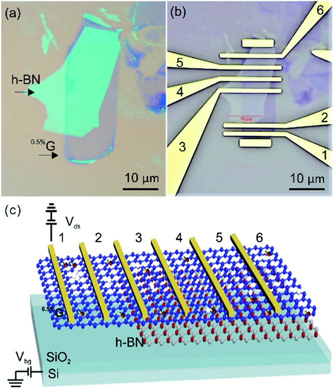 | ||
| Fig. 1 (a) Optical image of the fabricated h-BN/0.5%G heterostructure on SiO2. (b) The h-BN/0.5%G heterostructure device. Electrodes 1 and 2 define the SiO2/0.5%G FET device. Electrodes 1 and 3 define the 0.5%G on overlapped SiO2/h-BN hetero-substrate device. Electrodes 3 and 4 define the h-BN/0.5%G FET device. Distance between the electrodes 1–2 and 3–4 is 1.5 μm and 3 μm, respectively. (c) 3D illustration of the h-BN/0.5%G transistor device. | ||
Results and discussion
To gain structural information of 0.5%G, flakes of 0.5%G were deposited on HOPG surface and examined by scanning tunnelling microscopy (STM) under an ultra-high vacuum (10−10 mbar). The average height of a single 0.5%G flake was determined as 0.9 nm (Fig. 2a). At higher resolution, two different morphologies are detected in the 0.5%G flake, as depicted in Fig. 2b. The atomically resolved structure is assigned for the dark region while the resolution fades away in the bright region. The diffraction spots marked in dashed red indicate the hexagonal lattice of graphene in the dark regions, shown in Fig. 2c. The bright regions are caused by the oxygen-containing groups attached to the carbon lattice, which breaks the lattice periodicity of graphene and subsequently lead to no apparent diffraction feature in the reciprocal space (Fig. 2d).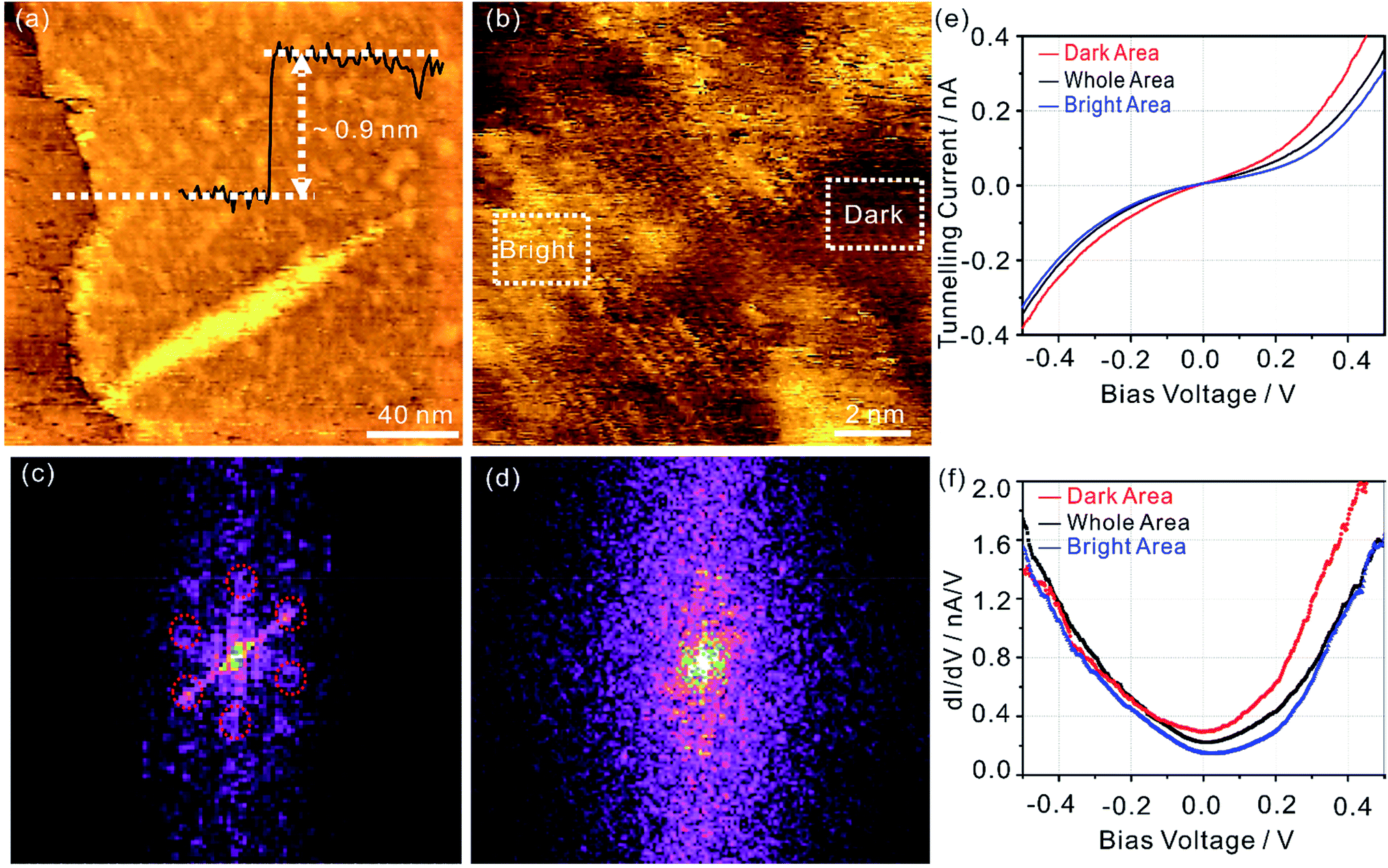 | ||
| Fig. 2 (a) Overview STM topographic image of the 0.5%G on highly oriented pyrolytic graphite (HOPG) substrate (200 nm × 200 nm; It = 0.6 nA, Vs = −0.5 V). The inset is the height profile of the 0.5%G flake. (b) STM topographic image of the 0.5%G (12 nm × 12 nm; It = 0.4 nA, Vs = −0.3 V). (c) and (d) Fast Fourier transform (FFT) images of the dark region and bright region in (b), respectively. (e) and (f) I (V) spectrum (averaged over >100 single spectra) and corresponding dI/dV curves recorded at the dark area (red curve), bright area (blue curve) and whole area (black curve), respectively. | ||
Atomic scale electronic properties of 0.5%G were explored using scanning tunnelling spectroscopy (STS). Fig. 2e displays the I (V) spectrum of the 0.5%G surface. Compared to the tunnelling current at the dark region, there exists an apparent suppression of current at the bright region owing to a lower conductivity in the distorted graphene lattices. For the averaged I (V) spectra of the whole area, the metallic behaviour of the 0.5%G flake is found. This phenomenon is also confirmed by the differential conductivity (dI/dV) curves in Fig. 2f. The Dirac point is determined from the minimum value in dI/dV curves. The Dirac point in dark region is located at 0.0 V, suggesting low impurity-related doping level. In contrast, the bright regions exhibit a positive shift of the Dirac point of about 50 mV, likely due to the presence of oxygen groups. For the entire scanned areas, the 0.5%G flake exhibits a p-type electronic doping feature with the average Dirac point at about 20 mV.
For the fabrication of the heterostructure of h-BN/0.5%G or SiO2/0.5%G, flakes of oxo-G were first deposited on SiO2 substrate by Langmuir–Blodgett technique,29 as shown in Fig. 3a. Then 0.5%G flakes were prepared by reduction using vapor of HI/TFA (in inset of Fig. 3b).30 The h-BN flakes used in this study were exfoliated from h-BN single crystals.31 Next, the heterostructures of h-BN/0.5%G or SiO2/0.5%G were prepared by a dry transfer technique.32
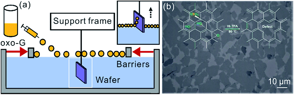 | ||
| Fig. 3 (a) Schematic illustration of Langmuir–Blodgett assembly of oxo-G single layers. (b) Optical image of collected 0.5%G flakes on a silicon wafer with 300 nm SiO2, obtained after hydroiodic acid (HI) and trifluoroacetic acid (TFA) reduction as shown in the inset. | ||
Fig. 4a shows an AFM image of a h-BN/0.5%G heterostructure, which consists of SiO2 substrate with multilayer h-BN flake and a monolayer 0.5%G flake (∼25 × 10 μm2) partially covering the h-BN. The AFM image in Fig. 4b, obtained within the marked area in Fig. 4a, revealed that the transfer process induced wrinkles and folds in 0.5%G. The height profile of the single 0.5%G flake on SiO2 is shown in Fig. 4c (compare Fig. S1†) and depicts a thickness of about 2 nm. This height is much thicker than 0.9 nm measured by STM for similar monolayer 0.5%G on HOPG. A major plausible reason is that e.g. water molecules are inevitably adsorbed on the hydrophilic SiO2 surface (treated by O2 plasma) leading to an approximately nanometer-thick hydrogen-bonded water layer and cleaved oxo-groups captured between SiO2 and 0.5%G.33 In contrast, although small amounts of polymer residues are likely trapped between h-BN and 0.5%G, the measured thickness of the same 0.5%G flake on h-BN is ∼1 nm as shown in Fig. 4c, which is almost the same result as the thickness determined by STM. The 0.5%G flake on ∼6 nm thick h-BN (Fig. 4c) possesses a lower roughness (∼0.5 nm) than on SiO2 (∼1 nm). Therefore, h-BN, as a passivation layer, can not only negate the influence of trapped water on graphene, but also improves accuracy in the AFM thickness measurements of monolayer 2D flakes.
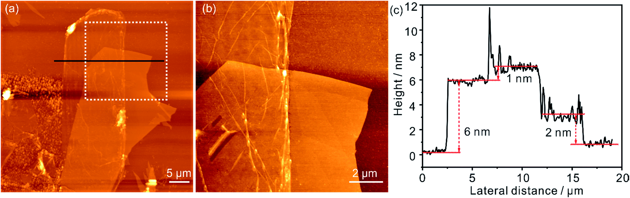 | ||
| Fig. 4 (a) AFM image of a h-BN/0.5%G heterostructure on a Si/SiO2 substrate. (b) AFM image obtained from the area within the white square in (a). (c) Height profiles of 0.5%G on SiO2, 0.5%G on h-BN and h-BN layer, which are corresponding to the black lines in (b). | ||
Average Raman spectra of the 0.5%G supported by SiO2 and h-BN, respectively, are shown in Fig. 5a. The primary peaks are the D peak near 1340 cm−1, the G peak near 1555–1557 cm−1 and the 2D peak near 2667 cm−1. The D peak of 0.5%G on each interface is mainly activated by defects in the carbon skeletons. The G and 2D peaks closely relate to the quality of graphene. The almost unchanged positions of the three peaks indicate that wrinkles and residual polymers induced during the transfer processes do not produce obvious doping effect on the single layer 0.5%G. We use scatter plots of ID/IG versus Γ2D to further confirm the quality of the 0.5%G in Fig. 5b. For the 0.5%G on h-BN, the ID/IG ratio is about 3.3, within the standard deviation of the ID/IG ratio of 3.1 determined on SiO2. Based on the model introduced by Lucchese and Cançado et al.,25,26 the density of lattice defects is related to 0.5% for the devices on h-BN and SiO2. This density of defects relates to the average distance between defects of around 3 nm. The related defect density (nD) is 4.0 × 1012 cm−2 on h-BN and SiO2, respectively, calculated from the equation nD (cm−2) = 1014/(πL2D).25 The Γ2D of the Raman 2D band is sensitive to the presence of defects. For the monolayer 0.5%G on h-BN, only a slightly smaller Γ2D of ∼70 cm−1 is observed than on SiO2 (∼72 cm−1). The same monolayer 0.5%G, partially deposited on SiO2 and h-BN, presents almost the same Γ2D. Therefore, the quality of the investigated flake is the same on SiO2 and h-BN, respectively.
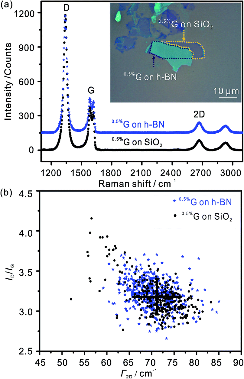 | ||
| Fig. 5 Statistical Raman microscopy measured with each pixel corresponding to an area of ∼0.7 × 0.7 μm2 at 532 nm laser excitation wavelength. The laser power is below 1 mW to avoid heating induced by laser. (a) Average Raman spectra of 0.5%G on SiO2 and h-BN. (b) ID/IG ratio vs. Γ2D. | ||
Reference experiments to determine the contact resistance were conducted using four-probe measurements. The surface resistance is determined to roughly 21 kOhm in four-probe configuration and 23.5 kOhm in two-probe configuration (Fig. S2†). Thus, further investigations were conducted in two-probe configuration under ambient conditions. For our transport measurements, we prepared one device with monolayer 0.5%G on SiO2 substrate (Fig. S3†), two devices with the same monolayer 0.5%G flake that are in part on SiO2 and on h-BN (Fig. 1 and S4†) and one device with monolayer 0.5%G on h-BN substrate (Fig. S5†). The patterning of the electrodes was achieved by standard electron beam lithography processing and subsequent deposition of 5 nm Cr/70 nm Au by thermal evaporation. The electrical performance of the 0.5%G flake on h-BN and SiO2, respectively, is summarised in Table 1. The resistance of 0.5%G on h-BN and SiO2 measured at Vbg = 0 V ranges widely, from 5.0 kΩ to 34.4 kΩ. But the resistances are significant lower compared to >106 Ω reported for similar devices.17
| Resistance/kΩ | Mobility/cm2 V−1 s−1 | Dirac point voltage/V | Channel length/μm | |
|---|---|---|---|---|
| a Reference device of 0.5%G on SiO2, see Fig. S3 (channel: 1–2).b Reference device of 0.5%G on SiO2, see Fig. S3 (channel: 2–3).c Reference device of 0.5%G on SiO2, see Fig. S4 (channel: 1–2).d Reference device of 0.5%G on h-BN, see Fig. S4 (channel: 3–4).e Reference device of 0.5%G on h-BN, see Fig. S5 (channel: 1–2). | ||||
| h-BN/0.5%G | 34.4 | 5.6 | ∼20 | 3 |
| SiO2/0.5%G | 15.6 | 11.6 | >43 | 1.5 |
| SiO2/0.5%G a | 5.0 | 14.2 | >50 | 3 |
| SiO2/0.5%G b | 5.7 | 14.5 | >50 | 3 |
| SiO2/0.5%G c | 6.8 | 7.4 | >60 | 2 |
| h-BN/0.5%G d | 18.7 | 5.3 | ∼37 | 2 |
| h-BN/0.5%G e | 32.5 | 8.5 | ∼22 | 1.5 |
Transfer curves (Ids–Vds) of 0.5%G on h-BN is shown in Fig. 6a. The Dirac points are located at around +20 V. The hysteresis effect of the 0.5%G on h-BN is observed in ambient environment for sweeping continuously from −50 to 50 V in forward direction and then back to −50 V (backward direction). From the red dashed lines presented in Fig. 6a, a room-temperature hole mobility (μh) of 5.6 cm2 V−1 s−1 is extracted using the equation μ = (L/W) × (1/(CoxVds)) × (dIds/dVbg),34 where Cox = 1.15 × 10⁻⁸ F cm−2. As the output curves (Ids–Vds) exhibit ohmic behaviour (Fig. 6b) we conclude that there is no Schottky contact between 0.5%G and metal electrodes. For the 0.5%G deposited on the overlapped SiO2-h-BN hetero-substrate (transport measurements performed between electrodes 2 and 4, shown in Fig. 1c), we observe only p-type character of the Ids–Vds curves with the Dirac point shifted to about +30 V (Fig. 6c).
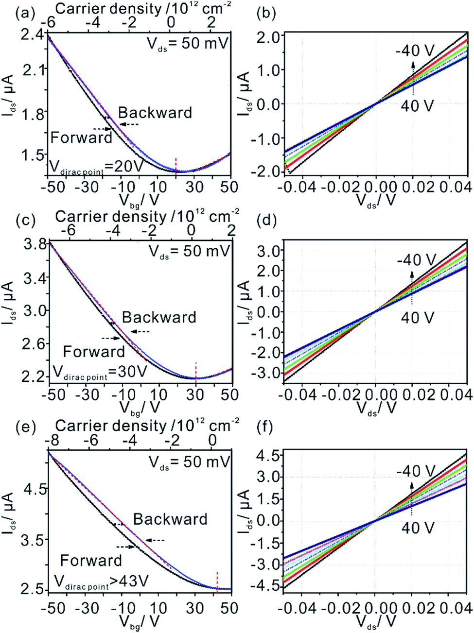 | ||
| Fig. 6 (a), (c) and (e) Transfer characteristics under ambient conditions for 0.5%G on h-BN, overlapped SiO2/hBN hetero-substrate and SiO2 with Vds = 50 mV. The gate voltage is swept continuously from −50 to 50 V and back to −50 V. (b), (d) and (f) Related Ids–Vds curves acquired for Vbg values from −40 V to 40 V in steps of 10 V. | ||
In contrast to 0.5%G on h-BN and overlapped SiO2-h-BN hetero-structure, the 0.5%G on SiO2 exhibits unipolar p-type character (Fig. 6e). The point of the minimum conductivity in the Ids–Vbg curve is not observed and the Dirac point moves to higher positive voltage (>43 V). Obviously, electrical transport of the 0.5%G on SiO2 is completely governed by holes with hole mobility μh estimated to about 11.6 cm2 V−1 s−1. In addition, the Ids–Vbg curves exhibit an increase of hysteresis in SiO2/0.5%G device with a shift of Vbg (ΔVbg ≈ 7.3 V) between the forward and reverse sweeps, compared to the h-BN/0.5%G device with ΔVbg ≈ 2.6 V. Substrate change from h-BN to SiO2 induces trapped holes with density higher than 1.6 × 1012 cm−2 using Δnt = ΔVDirac point (Cox/q),2 where q is the elementary charge, ΔVDirac point > 43–20 = 23 V. In general, a high density of charge traps can cause hysteresis and lead to reduced mobility of graphene samples.35 However, as summarized in Table 1, mobility values on SiO2 are higher and the resistance is lower than on h-BN. The main reason for that contradictory finding is that for 0.5%G defects are the dominant scatterers reducing the carrier mobility. This is consistent with Raman results of Fig. 5b. As further reference experiments we conducted transport measurements of defective graphene, here 0.8%G on SiO2. As shown in Fig. S6,† due to the higher density of defects the hole mobility values are 0.6 cm2 V−1 s−1 in ambient and 0.9 cm2 V−1 s−1 in vacuum. However, the Dirac point shifts only from 60 V in ambient to 30 V in vacuum. Those results are in agreement with the STS measurements, which indicate p-doping of 0.5%G in vacuum. It could however be expected that oxo-groups with −I and −M effects,2,3 decorating the rims of vacancy defects, may be responsible for trapping hole carriers. However, the experimental results, such as transport and AFM measurements, give evidence that p-doping is strongly induced by the SiO2 substrate and cleaved oxo-species, such as water or organosulfate, which are trapped between SiO2 and 0.5%G. Therefore, based on the AFM height determination on SiO2, the knowledge about the chemical structure and the reduction mechanism of oxo-G to 0.5%G we propose that molecules, such as water or hydrogensulfate stemming from oxo-G (Fig. 7a) are trapped between the SiO2 substrate surface and 0.5%G (Fig. 7b). In comparison, h-BN is affected by the local polarity of h-BN/0.5%G. As a result, spurious dopant molecules may get squeezed out (Fig. 7c), as is also supported by the measured height and roughness results determined by AFM.
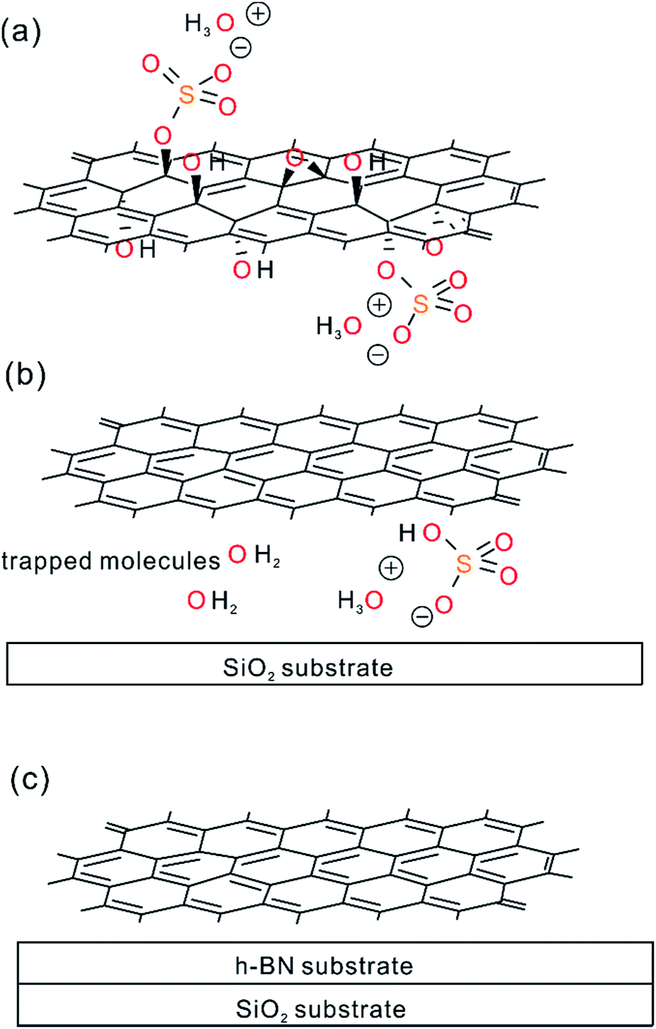 | ||
| Fig. 7 Proposed model of trapped species upon cleavage of oxo-groups upon reduction and influence of substrate. (a) Chemical sketch of the structure of oxo-G with the graphene lattice decorated by hydroxyl-, epoxy- and organosulfate groups. (b) 0.5%G prepared by chemical reduction of oxo-G; covalently bound oxo-groups are cleaved and at least partially trapped between 0.5%G and the SiO2 substrate. (c) 0.5%G on h-BN; cleaved oxo-groups may not be trapped between h-BN and 0.5%G because they are squeezed out. | ||
Conclusions
0.5%G is a p-doped material and defects determine the scattering of charge carriers. Using h-BN as substrate leads to less trapped molecules, which are responsible for p-doping. In this regard, most likely hydrogen-bonded water and other cleaved oxo-species are captured between SiO2 and 0.5%G causing p-doping, as a consequence of chemical reduction of oxo-G. The ambipolar behaviour with VDirac point of +20 V was therefore observed for the h-BN/0.5%G structure while unipolar p-type response was shown for the same 0.5%G flake on SiO2. Transfer characteristics show a reduction of hysteresis in the h-BN/0.5%G. The mobility of the SiO2/0.5%G is determined to 7.4–14.5 cm2 V−1 s−1 and for h-BN/0.5%G to 5.6–8.5 cm2 V−1 s−1 at ambient conditions.Conflicts of interest
There are no conflicts to declare.Acknowledgements
This research is supported by the China Scholarship Council (CSC), the Deutsche Forschungsgemeinschaft (DFG, German Research Foundation), project number 392444269 and 249559513, and ERC Grant No. 639739.References
- D. C. Marcano, D. V. Kosynkin, J. M. Berlin, A. Sinitskii, Z. Sun, A. Slesarev, L. B. Alemany, W. Lu and J. M. Tour, ACS Nano, 2010, 4, 4806–4814 CrossRef CAS PubMed.
- Y. Zhu, S. Murali, W. Cai, X. Li, J. W. Suk, J. R. Potts and R. S. Ruoff, Adv. Mater., 2010, 22, 3906–3924 CrossRef CAS PubMed.
- S. Eigler, M. Enzelberger-Heim, S. Grimm, P. Hofmann, W. Kroener, A. Geworski, C. Dotzer, M. Rockert, J. Xiao, C. Papp, O. Lytken, H. P. Steinrück, P. Müller and A. Hirsch, Adv. Mater., 2013, 25, 3583–3587 CrossRef CAS PubMed.
- D. R. Dreyer, S. Park, C. W. Bielawski and R. S. Ruoff, Chem. Soc. Rev., 2010, 39, 228–240 RSC.
- H.-J. Shin, K. K. Kim, A. Benayad, S.-M. Yoon, H. K. Park, I.-S. Jung, M. H. Jin, H.-K. Jeong, J. M. Kim, J.-Y. Choi and Y. H. Lee, Adv. Funct. Mater., 2009, 19, 1987–1992 CrossRef CAS.
- O. M. Slobodian, P. M. Lytvyn, A. S. Nikolenko, V. M. Naseka, O. Y. Khyzhun, A. V. Vasin, S. V. Sevostianov and A. N. Nazarov, Nanoscale Res. Lett., 2018, 13, 139 CrossRef.
- H. F. Liang, C. T. G. Smith, C. A. Mills and S. R. P. Silva, J. Mater. Chem. C, 2015, 3, 12484–12491 RSC.
- M. A. Velasco-Soto, S. A. Pérez-García, J. Alvarez-Quintana, Y. Cao, L. Nyborg and L. Licea-Jiménez, Carbon, 2015, 93, 967–973 CrossRef CAS.
- S. Pei and H.-M. Cheng, Carbon, 2012, 50, 3210–3228 CrossRef CAS.
- H. L. Guo, X. F. Wang, Q. Y. Qian, F. B. Wang and X. H. Xia, ACS Nano, 2009, 3, 2653–2659 CrossRef CAS PubMed.
- K. W. Silverstein, C. E. Halbig, J. S. Mehta, A. Sharma, S. Eigler and J. M. Mativetsky, Nanoscale, 2019, 11, 3112–3116 RSC.
- S. Yang, M. R. Lohe, K. Müllen and X. L. Feng, Adv. Mater., 2016, 28, 6213–6221 CrossRef CAS PubMed.
- B. Butz, C. Dolle, C. E. Halbig, E. Spiecker and S. Eigler, Angew. Chem., Int. Ed., 2016, 55, 15771–15774 CrossRef CAS PubMed.
- F. Grote, C. Gruber, F. Börrnert, U. Kaiser and S. Eigler, Angew. Chem., Int. Ed., 2017, 56, 9222–9225 CrossRef CAS PubMed.
- B. Radisavljevic, A. Radenovic, J. Brivio, V. Giacometti and A. Kis, Nat. Nanotechnol., 2011, 6, 147–150 CrossRef CAS PubMed.
- K. Kim, J. Y. Choi, T. Kim, S. H. Cho and H. J. Chung, Nature, 2011, 479, 338–344 CrossRef CAS PubMed.
- C. Gòmez-Navarro, R. T. Weitz, A. M. Bittner, M. Scolari, A. Mews, M. Burghard and K. Kern, Nano Lett., 2007, 7, 3499–3503 CrossRef PubMed.
- C. Y. Su, Y. P. Xu, W. J. Zhang, J. W. Zhao, A. P. Liu, X. H. Tang, C. H. Tsai, Y. Z. Huang and L. J. Li, ACS Nano, 2010, 4, 5285–5292 CrossRef CAS PubMed.
- J. K. Wassei and R. B. Kaner, Mater. Today, 2010, 13, 52–59 CrossRef CAS.
- Y. L. Wang, Y. A. Chen, S. D. Lacey, L. S. Xu, H. Xie, T. Li, V. A. Danner and L. B. Hu, Mater. Today, 2018, 21, 186–192 CrossRef CAS.
- R. Negishi, M. Akabori, T. Ito, Y. Watanabe and Y. Kobayashi, Sci. Rep., 2016, 6, 28936 CrossRef CAS PubMed.
- G. Cassabois, P. Valvin and B. Gil, Nat. Photonics, 2016, 10, 262 CrossRef CAS.
- C. R. Dean, A. F. Young, I. Meric, C. Lee, L. Wang, S. Sorgenfrei, K. Watanabe, T. Taniguchi, P. Kim, K. L. Shepard and J. Hone, Nat. Nanotechnol., 2010, 5, 722–726 CrossRef CAS PubMed.
- C. E. Halbig, R. Lasch, J. Krull, A. S. Pirzer, Z. P. Wang, J. N. Kirchhof, K. I. Bolotin, M. R. Heinrich and S. Eigler, Angew. Chem., Int. Ed., 2019, 58, 3599–3603 CrossRef CAS PubMed.
- L. G. Cançado, A. Jorio, E. H. Ferreira, F. Stavale, C. A. Achete, R. B. Capaz, M. V. Moutinho, A. Lombardo, T. S. Kulmala and A. C. Ferrari, Nano Lett., 2011, 11, 3190–3196 CrossRef PubMed.
- M. M. Lucchese, F. Stavale, E. H. M. Ferreira, C. Vilani, M. V. O. Moutinho, R. B. Capaz, C. A. Achete and A. Jorio, Carbon, 2010, 48, 1592–1597 CrossRef CAS.
- P. Vecera, S. Eigler, M. Kolesnik-Gray, V. Krstic, A. Vierck, J. Maultzsch, R. A. Schäfer, F. Hauke and A. Hirsch, Sci. Rep., 2017, 7, 45165 CrossRef CAS PubMed.
- A. Naumov, F. Grote, M. Overgaard, A. Roth, C. E. Halbig, K. Nørgaard, D. M. Guldi and S. Eigler, J. Am. Chem. Soc., 2016, 138, 11445–11448 CrossRef CAS PubMed.
- L. J. Cote, F. Kim and J. Huang, J. Am. Chem. Soc., 2009, 131, 1043–1049 CrossRef CAS PubMed.
- S. Eigler, S. Grimm, M. Enzelberger-Heim, P. Müller and A. Hirsch, Chem. Commun., 2013, 49, 7391–7393 RSC.
- R. V. Noorden, Nature, 2012, 483, S32–S33 CrossRef.
- X. Ma, Q. Liu, D. Xu, Y. Zhu, S. Kim, Y. Cui, L. Zhong and M. Liu, Nano Lett., 2017, 17, 6961–6967 CrossRef CAS.
- M. J. Lee, J. S. Choi, J. S. Kim, I. S. Byun, D. H. Lee, S. Ryu, C. Lee and B. H. Park, Nano Res., 2012, 5, 710–717 CrossRef CAS.
- F. Schwierz, Nat. Nanotechnol., 2010, 5, 487–496 CrossRef CAS PubMed.
- A. D. Bartolomeo, F. Giubileo, F. Romeo, P. Sabatino, G. Carapella, L. Iemmo, T. Schroeder and G. Lupina, Nanotechnology, 2015, 26, 475202–475210 CrossRef.
Footnote |
| † Electronic supplementary information (ESI) available. See DOI: 10.1039/c9ra09197a |
| This journal is © The Royal Society of Chemistry 2019 |