
 Open Access Article
 This Open Access Article is licensed under a
 Creative Commons Attribution 3.0 Unported Licence
Thermal conductivity suppression in GaAs–AlAs core–shell nanowire arrays
Taneli
Juntunen
 *a,
Tomi
Koskinen
a,
Vladislav
Khayrudinov
a,
Tuomas
Haggren
b,
Hua
Jiang
c,
Harri
Lipsanen
a and
Ilkka
Tittonen
a
*a,
Tomi
Koskinen
a,
Vladislav
Khayrudinov
a,
Tuomas
Haggren
b,
Hua
Jiang
c,
Harri
Lipsanen
a and
Ilkka
Tittonen
a
aDepartment of Electronics and Nanoengineering, Aalto University, P.O. Box 13500, FI-00076 Aalto, Finland. E-mail: taneli.juntunen@aalto.fi
bDepartment of Electronic Materials Engineering, Research School of Physics and Engineering, The Australian National University, Canberra, ACT 2601, Australia
cDepartment of Applied Physics, Aalto University, P.O. Box 15100, FI-00076 Aalto, Finland
First published on 28th October 2019
Abstract
Semiconductor nanowire heterostructures have been shown to provide appealing properties for optoelectronics and solid-state energy harvesting by thermoelectrics. Among these nanoarchitectures, coaxial core–shell nanowires have been of primary interest due to their electrical functionality, as well as intriguing phonon localization effects in the surface-dominated regime predicted via atomic simulations. However, experimental studies on the thermophysical properties of III–V semiconductor core–shell nanowires remain scarce regardless of the ubiquitous nature of these compounds in solid-state applications. Here, we present thermal conductivity measurements of the arrays of GaAs nanowires coated with AlAs shells. We unveil a strong suppression in thermal transport facilitated by the AlAs shells, up to ∼60%, producing a non-monotonous dependence of thermal conductivity on the shell thickness. Such translation of the novel heat transport phenomena to macroscopic nanowire arrays paves the way for rational thermal design in nanoscale applications.
Semiconductor nanowires (NWs) have emerged as pivotal low-dimensional systems for thermoelectric applications. Compared to their bulk counterparts, experiments have proposed a significant enhancement in the thermoelectric efficiency of NWs, based largely on the strong thermal conductivity suppression of one to two orders of magnitude in Si and SiGe alloy NWs with a diameter of few tens of nanometers.1–3 In contrast, studies on, e.g., Bi2Te3
![[thin space (1/6-em)]](https://www.rsc.org/images/entities/char_2009.gif) 4 and InSb5,6 NWs demonstrated a decrease in the overall thermoelectric performance in comparison with their bulk counterparts, suggesting that a high degree of control over the thermal and electrical properties of the NWs is required.
4 and InSb5,6 NWs demonstrated a decrease in the overall thermoelectric performance in comparison with their bulk counterparts, suggesting that a high degree of control over the thermal and electrical properties of the NWs is required.
Nanowire heterostructures provide a potential route for further optimizing the thermophysical properties of NWs. Apart from thermal conductivity reduction by the classical size effect, ultimately capped by the diffusive Casimir limit, NWs covered with structural resonances such as branches7 and shells8–10 have attracted attention due to the additional emergent thermal wave phenomena in these systems. Such effects rely on the suppression of phonon modes in the main wire through their hybridization with non-propagating localized modes of the resonant structures. Hu et al.11,12 found a drastic 75% reduction in the thermal conductivity of Si–Ge core–shell nanowires (CSNWs), followed by Chen et al.13 with 25% in a similar study. Such manifestation of phonon coherence is a promising route for thermal engineering; however, it remains largely unexplored through experiments.
Surprisingly, to this end no experimental results on the thermal conductivity of III–V semiconductor CSNWs have been reported and regardless of the established position of these compounds in optoelectronic14 and thermoelectric6 applications, the existing work remains limited to individual Ge–Si15 (Si–Ge16) and Bi–Te17 CSNWs. In fact, even pure III–V semiconductor NWs remain relatively scarcely studied, with InAs,18–20 GaAs,21,22 and InSb.5,6 As an exemplary consequence, the low-temperature measurements by Fon et al.21 remain the only reference for theoretical predictions on the thermal conductivity of GaAs NWs.23,24
As technological applications ultimately necessitate the implementation of macroscopic arrays of NWs embedded in a low-thermal conductivity matrix,25 we present thermal conductivities of GaAs NW and GaAs–AlAs CSNW arrays, grown by metalorganic vapor-phase epitaxy (MOVPE) and measured via the nanosecond transient thermoreflectance (ns-TTR) method. Since an optical pump–probe method is used for thermal characterization, the samples are planarized by embedding the NWs in a spin-on-glass host matrix to form a composite. A prominent advantage of the utilization of macroscopic NW arrays is the inherent ensemble averaging taking place upon characterizing a single sample, mitigating the effect of structural variation at the level of individual NWs. Such an approach has been applied recently to, e.g., InAs,18 Bi2Te3,26,27 BiSbTe alloy,28 and Si NWs with various surface modifications.28–32
The NW growth and sample preparation steps are shown in Fig. 1(a). GaAs core–shell NWs are synthesized on p-GaAs (111)B substrates using the Au nanoparticle-assisted vapor–liquid–solid (VLS) growth method. To determine the thermal contribution of the NWs in the composite experimentally, both sufficient areal density and a low thermal conductivity host material are required. Substrate functionalization is necessary for controlling the self-assembly of the Au catalyst particles, and is conventionally achieved using poly-L-lysine (PLL) promoting nanoparticle adhesion on the substrate surface. However, PLL was found to yield modest particle densities for sufficient areal density of NWs. To achieve reliable thermal analysis, poly(diallyldimethylammonium chloride) (PDDAC) was instead found to significantly increase the nanoparticle density while retaining the uniform growth of the NW arrays.33 The substrates are treated with PDDAC solution (20 wt%) for 20 min. Subsequently, a 40 nm diameter colloidal Au nanoparticle solution (BBI International, UK) is applied onto the sample surface for 30 min before drying with nitrogen and transferred into a horizontal flow atmospheric pressure MOVPE system. Prior to the growth, the substrates are annealed in situ at 600 °C for 10 minutes under hydrogen flow to desorb surface contaminants as measured by using a thermocouple in the lamp-heated graphite susceptor.34,35 Trimethylgallium (TMGa) and tertiarybutylarsene (TBAs) are used as precursors for GaAs core growth, and trimethylaluminum (TMAl) and TBAs are used for AlAs shells. Hydrogen is used as a carrier gas, resulting in a total reactor gas flow of ∼5 l min−1 (SLM). The growth temperature of GaAs NW cores is fixed at 465 °C for 40 s with TMGa and TBAs flows of 10.8 μmol min−1 and 270 μmol min−1, respectively, and a nominal V/III ratio of 25. The ∼55 nm diameter cores are then coaxially grown for 50 s at 650 °C under similar conditions for a subset of samples to yield NWs of approximately 100 nm in diameter. AlAs NW shells are grown at 650 °C for 1–50 s (depending on the desired thickness) with a nominal V/III ratio of 9.4, and TMAl and TBAs flows of 28.8 μmol min−1 and 270 μmol min−1, respectively. Finally, a subset of AlGaAs-alloyed shell NWs is also investigated, grown with a nominal V/III ratio of 10 and TMAl, TMGa, and TBAs flows of 21.6 μmol min−1, 25.3 μmol min−1 and 468 μmol min−1, respectively. The structural analysis of the NW arrays is performed using a scanning electron microscope (SEM), and the areal packing densities of NWs are determined by image analysis with a typical fractional uncertainty of ∼2–8%.
 | ||
| Fig. 1 Fabrication and thermal modeling of the macroscopic NW arrays. (a) Core–shell NWs are grown by MOVPE from self-assembled Au catalyst particles and partly embedded in a methyl siloxane-based spin-on-glass (SOG). The samples are planarized using chemical mechanical polishing (CMP), and a 200 nm Au heat transducer film is e-beam evaporated on the sample surface for room temperature optical pump–probe measurement. Inset: MOVPE growth processes of the investigated NWs with two core diameters. (b) Thermal finite-element method (FEM) model of the SOG/NW composite structure, accounting for the three-dimensional sample geometry. (c) The one-dimensional (1D) heat transfer model fitted to the measured thermoreflectance signal of SOG, as well as FEM reproduction of the measurement. (d) Comparison between the effective thermal conductivity calculated from FEM input (κsog = 0.35 W m−1 K−1) and the resulting thermal conductivities from the 1D heat transfer model with varying NW diameter d (nm), interfacial thermal resistance Rsog/nw (K m2 GW−1), NW areal fraction x (−), and NW thermal conductivity κnw (W m−1 K−1). | ||
Fig. 2(a) and (b) show tilted-view SEM micrographs of the GaAs NWs with and without radial AlAs shell growth, respectively. A typical areal density of ∼6% is achieved through PDDAC functionalization of the substrates. A variation of ∼15% from the average diameter and a slight tapering of the NWs inherent for the non-selective growth are observed and accounted for in the thermal conductivity analysis. A high-resolution transmission electron microscopy (HRTEM) micrograph of a single GaAs NW is shown in Fig. 2(c). The micrographs confirm the [111] growth direction of the wires, as well as the pristine zinc blende crystalline structure as revealed by the HRTEM diffraction pattern. Fig. 2(d) shows a magnification of the GaAs NW surface, presenting the highly smooth surface with a sub-nm roughness. The respective analysis of the GaAs–AlAs CSNWs confirmed single-crystalline coaxial growth together with a similar surface topography, suggesting that the core–shell interface adopts the high structural order of the NW surface.
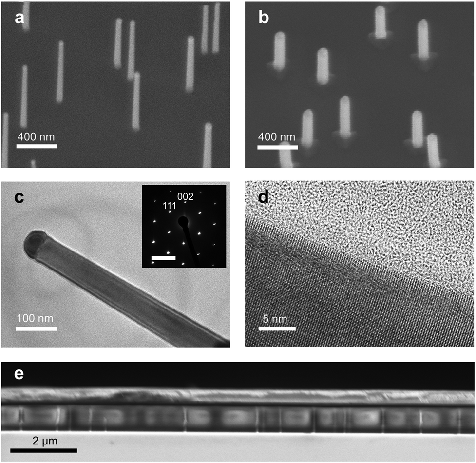 | ||
Fig. 2 SEM and HRTEM characterization of the NWs. (a and b) SEM micrographs of the GaAs NWs and GaAs–AlAs CSNWs grown by MOVPE, respectively (tilt angle 30°). CSNW shell thickness is controlled by growth time, here produced via 5 s (∼20 nm) coaxial growth. (c) HRTEM micrograph of a GaAs NW. Inset: Diffraction pattern of the zinc blende crystalline structure taken along the [1![[1 with combining macron]](https://www.rsc.org/images/entities/char_0031_0304.gif) 0] zone axis (scale bar: 4 nm−1). (d) Magnification of the NW surface. (e) Sample cross-section of GaAs NWs (d ≈ 55 nm) embedded in SOG, planarized, and coated with the Au transducer film. 0] zone axis (scale bar: 4 nm−1). (d) Magnification of the NW surface. (e) Sample cross-section of GaAs NWs (d ≈ 55 nm) embedded in SOG, planarized, and coated with the Au transducer film. | ||
To prepare samples for thermal characterization, the NW arrays are embedded in a methyl siloxane-based spin-on-glass (SOG, Honeywell Accuglass T-12) by spin-coating. After curing at elevated temperatures, the resulting SOG film is on average 600 nm thick, leaving the tips of the 1 μm NWs exposed. To obtain a smooth surface, the samples are subsequently planarized by chemical mechanical polishing (CMP, Struers) for 5 min under 5 N pressing force using a 40 nm silica bead slurry as an abrasive medium. After washing, 20/200 nm of Ti/Au is deposited onto the sample surface via e-beam evaporation to act as a heat transducer for the optical pump–probe measurement. Fig. 2(e) shows a cleaved cross-sectional view of a sample prepared for measurement, exposing several NWs embedded in SOG. The SOG matrix provides voidless filling of the NW array, further protecting the embedded sections of the NWs during the CMP process.
The thermal diffusivity of the composite is measured by ns-TTR (Linseis) at room temperature as reported previously36 and averaged over six positions over the ∼1 cm2 sample surface. In brief, the surface of the sample is heated by an 8 ns infrared laser pulse. Provided that the reflectance of the Au transducer film is linearly proportional to its surface temperature, the thermal transient probed by a laser diode may be fitted to a one-dimensional (1D) heat transmission model. In the model, we treat the composite as a homogeneous material in exploiting the widely utilized effective medium model (EMM), within which the volumetric heat capacity and thermal conductivity κc of the composite are assumed as a volumetric average of the NWs and the SOG matrix. Thus, the thermal conductivity of NWs is back-traced as κnw = x−1 (κc − [1 − x]κsog), where x denotes the areal fraction of NWs in the sample.37 A standard Gaussian error propagation analysis is carried out on the basis of experimental uncertainties of areal density and the thermal conductivity measurement.
The validity of the 1D heat transfer model is explored through finite-element method (FEM, Comsol Multiphysics) simulations, explicitly accounting for the NW geometry and the heterogeneity of the sample in the periodic in-plane direction, as shown in Fig. 1(b). The size of the simulation domain is set to correspond to the NW areal density. Fig. 1(c) shows a measured signal from the SOG together with the 1D heat transfer model and a FEM reproduction with a thermal conductivity of κsog = 0.35 ± 0.03 W m−1 K−1 in sound agreement. Furthermore, the measured value is consistent with prior measurements.29 The validity of the 1D heat transfer model is further tested with various system parameters, including NW diameter d = 50–100 nm, areal density x = 0.01–0.10, and thermal conductivity κnw = 1–10 W m−1 K−1. Fig. 1(d) shows the relationship between the effective thermal conductivity based on the FEM input and the 1D heat model result from analyzing the produced signal, showing a strong agreement within the relevant parameter space and roughly 10% uncertainty (shaded region). Moreover, significant thermal interface resistances of R = 100 K m2 GW−1 were imposed both between the NWs and the SOG matrix (Rsog/nw) and the metal transducer and the SOG/NW composite (not shown), resulting in a negligible effect owing to the relatively low thermal conductivity of the investigated composites. EMM is therefore highly justified for extracting the thermal conductivity of the NWs using the ns-TTR measurement.
Fig. 3 shows the measured thermal conductivities of pure GaAs NW arrays as well as those coated with an epitaxial shell. While pure GaAs NWs with two diameters of ∼55 nm and ∼100 nm were grown, the thin GaAs NWs without additional coaxial growth produce a rather low areal density of 1.5–2.0% and could not be reliably distinguished from the SOG matrix, further implying a low thermal conductivity of <5 W m−1 K−1. The thicker GaAs NWs with diameters of ∼100 nm, on the other hand, show a thermal conductivity of 6.6 W m−1 K−1 (Fig. 3(a)), calculated from the 0.8 W m−1 K−1 effective thermal conductivity of the SOG/NW composite. Calculation with a similar areal packing density and the bulk thermal conductivity of GaAs results in a corresponding effective thermal conductivity κc = 3.6 W m−1 K−1, compared to which the composite demonstrates a drastic (78%) reduction originating from nanoscale confinement of the GaAs constituent. The NW thermal conductivity is moderately lower than the broad range of 8–36 W m−1 K−1 reported by Soini et al.22 for individual GaAs nanowires (d ≈ 150 nm), obtained through micro-Raman measurements. The difference may be attributed to the high uncertainty in the micro-Raman technique, as well as difference in the NW diameter and surface geometry. To validate the thermal conductivity measured for pure GaAs NWs further, we compare the value to theoretical predictions as provided by the full Holland model40 in the Casimir limit τb−1 = vs/d, a phenomenological model proposed by Liang and Li,24 as well as results by Mingo38 and Martin et al.39 accounting for the full phonon dispersion of GaAs. Bulk phonon scattering rates within the Holland model are adopted after Chen and Tien,41 with the total (frequency-dependent) relaxation time calculated according to Matthiessen's rule
| τj−1 = τb−1 + τi−1 + τN,j−1 + τU,j−1, | (1) |
 | ||
| Fig. 3 (a) Thermal conductivity of GaAs nanowires. Lines represent predictions by the Holland model (solid), Mingo38 (dotted), interpolated results from Martin et al.39 (dash-dotted), and a phenomenological model by Liang and Li24 (dashed). (b) Thermal conductivity of GaAs–AlAs core–shell nanowires as a function of shell thickness (line as a guide for the eye). (c) Thermal conductivity of 105 nm diameter GaAs NWs with thin AlAs and AlGaAs shells. Reduction percentage is disclosed in parenthesis. The measurements are carried out at room temperature. | ||
From a simplistic effective medium perspective, an elemental substitution of GaAs with AlAs should be expected to increase the overall thermal conductivity, given the bulk values of 47 W m−1 K−1 and 91 W m−1 K−1 for GaAs and AlAs, respectively.43 Strikingly, the introduction of an AlAs shell on a thin GaAs NW is found to have the opposite effect on the thermal transport of the NWs, as shown in Fig. 3(b). Shell growth on GaAs NWs of d = 55 nm initially results in a drastic reduction of thermal conductivity as a function of shell thickness, measured up to ∼60% as compared to NWs with a minimal shell. However, the thermal conductivity shows a non-monotonous dependence on the shell thickness, as a thermal conductivity minimum is observed at a shell thickness of ∼30 nm. Above the minimum, thermal conductivity consistently increases with shell thickness. The transition between thermal conductivity suppression and increase suggests that AlAs shell growth on the GaAs NWs affects the transport properties in a non-trivial manner, showing characteristics of competing transport regimes mediated by the shell.
While several continuum models44–46 have been developed for thermophysical modeling of CSNWs, atomistic simulations have proved essential in capturing the competing transport effects in confined semiconductor heterostructures. Even though molecular and lattice dynamical simulations are computationally limited to nanowires of sub-20 nm diameter, we find a similarity between the proposed thermal conductivity reduction mechanisms and our data. In particular, several molecular dynamics (MD) studies on CSNWs have revealed a similar minimum in the shell thickness dependence of thermal conductivity as observed here.11–13 For instance, Chen et al.13 studied the behavior of Ge NWs coated with the higher thermal conductivity Si and found that the coating thickness achieving minimal thermal conductivity monotonically increases with the core diameter. The depth of the minimum is further increased by interfacial roughness between the core and the shell.
In these MD studies, the minimum has been attributed to the competing effects of decreasing thermal conductivity due to the localization of low-frequency phonons at the core–shell interface, and increasing thermal conductivity due to the reduced surface scattering as the surface-to-volume ratio of the NWs decreases with the increasing cross-sectional area. Localization of these low-frequency phonons results from the hybridization of the longitudinal propagating phonon modes and the confined non-propagating transverse modes, mediated by the vibrational mismatch between the core and the shell.8 Interfacial roughness, on the other hand, scatters high-frequency phonons with wavelength much less than the NW diameter.13
Prior experimental studies on CSNWs have also reported thermal conductivity reduction provoked by the shell. Kang et al.17 studied crystalline Bi NWs coated with 30 nm thick quasi-amorphous Te shells (κBi > κTe) and found that the reduction is strongly dependent on the core–shell interface roughness. The effect was thus attributed to the interfacial scattering, and also a considerable thermal conductivity reduction in CSNWs with smooth interfaces was observed. Wingert et al.15 additionally reported the possibility of localized low-frequency modes at the core–shell interface in the 10–20 nm Ge NWs coated with a 1–3 nm Si shell, further suggesting that the effect might be more prominent in the ultra-thin wires studied in the described MD work. In contrast, Hsiao et al.16 demonstrated the thermal conductivity reduction of comparatively thick Si–Ge NWs, proposing that the localization effect mediated by the shell would extend to much thicker coatings (>30 nm), and that the heterogeneous interface appears to induce phonon filtering in regions extending far from the core–shell interface. The emergence of a thermal conductivity minimum in the shell thickness dependence in Fig. 3(b) indeed offers additional insight and support for the proposed complex role of the interface in CSNWs. While interface scattering clearly affects thermal transport in experimentally realized CSNWs, the gradual thermal conductivity reduction with increasing the shell thickness suggests a coherent contribution to the thermal transport inhibition. Eventual thermal conductivity increase with the increasing shell thickness, on the other hand, is the expected consequence of the increasing phonon transmission in the AlAs shell region.
Finally, to gain more insight into the thermal conductivity reduction, we retain the overall diameter of ∼120 nm by introducing the thin AlAs as well as AlGaAs-alloyed shells onto GaAs NWs with diameters of ∼105 nm. As shown in Fig. 3(c), a higher thermal conductivity is measured despite the higher volumetric ratio of GaAs in the NWs and the higher number of atoms located in the proximity of the interface. Here, the 10–15 nm AlAs shell serves to reduce the thermal conductivity by ∼20%. A similar reduction is also observed in the AlGaAs surface-alloyed NWs within experimental uncertainty, suggesting that the thermal conductivity reduction induced by the thin shell is predominantly related to the Rayleigh-type scattering of high-frequency phonons with the characteristic τi ∝ ω−4 dependence.47 A more moderate reduction may thus result from the relative shift from resonant phonon inhibition to impurity scattering mediated by the shell in NWs with a thick GaAs core. The former is indeed expected to be mitigated with the increasing core diameter, resulting in thermal conductivity reduction primarily due to the interface and alloy scattering. A comparable reduction has also been observed in Si NW (d ≈ 100 nm) arrays with discrete surface doping of Ge.31
While GaAs–AlAs systems are most widely utilized in optoelectronics where advanced thermal engineering may facilitate the design of, e.g., improved-efficiency light-emitting diode (LED) CSNWs,48 our findings are also expected to translate to other III–V systems with thermoelectric potential. For instance, InSb and InAs-based NWs have attracted much interest for thermoelectric applications.5,6,38,49,50 InAs–InP CSNWs also exhibit an unusually high carrier mobility due to the introduction of an electron gas without promoting ionized impurity scattering,51 which together with the presented results provides a prospective system for a novel thermoelectric design.
In summary, we have measured the thermal conductivities of MOVPE grown GaAs NWs and GaAs–AlAs CSNW arrays using an optical pump–probe method. We establish the thermal conductivity of pure GaAs NWs, and reveal a strong suppression of thermal conductivity in GaAs NWs decorated with AlAs shells. CSNWs show a non-monotonous dependence on the shell thickness, suggesting a possible competition between coherent phonon suppression and reduction of surface scattering in increasing the diameter of the wire. Thus, CSNWs offer a potential structural building block for translating novel heat transport effects in the phonon confinement regime to macroscopic NW array-based energy harvesting and optoelectronic applications.
Conflicts of interest
There are no conflicts to declare.Acknowledgements
T. J. and V. K. acknowledge ELEC Doctoral School for financial support. V. K. further acknowledges the support from Walter Ahlström Foundation and Nokia Foundation. H. L. and I. T. would like to thank the Academy of Finland Flagship Programme (320167, PREIN). This work was performed, in part, within TransFlexTeg under European Union's Horizon 2020 Programme (No. 645241) and Academy of Finland Project No. 319018 in the facilities and with the technical support from Aalto University at Micronova Nanofabrication Centre.References
- A. I. Hochbaum, R. Chen, R. D. Delgado, W. Liang, E. C. Garnett, M. Najarian, A. Majumdar and P. Yang, Nature, 2008, 451, 163 CrossRef CAS PubMed.
- A. I. Boukai, Y. Bunimovich, J. Tahir-Kheli, J.-K. Yu, W. A. Goddard III and J. R. Heath, Nature, 2008, 451, 168 CrossRef CAS PubMed.
- E. K. Lee, L. Yin, Y. Lee, J. W. Lee, S. J. Lee, J. Lee, S. N. Cha, D. Whang, G. S. Hwang, K. Hippalgaonkar, A. Majumdar, C. Yu, B. L. Choi, J. M. Kim and K. Kim, Nano Lett., 2012, 12, 2918 CrossRef CAS.
- A. Mavrokefalos, A. L. Moore, M. T. Pettes, L. Shi, W. Wang and X. Li, J. Appl. Phys., 2009, 105, 104318 CrossRef.
- F. Zhou, A. L. Moore, M. T. Pettes, Y. Lee, J. H. Seol, Q. L. Ye, L. Rabenberg and L. Shi, J. Phys. D: Appl. Phys., 2009, 43, 025406 CrossRef.
- S. Yazji, M. Y. Swinkels, M. De Luca, E. A. Hoffmann, D. Ercolani, S. Roddaro, G. Abstreiter, L. Sorba, E. P. A. M. Bakkers and I. Zardo, Semicond. Sci. Technol., 2016, 31, 064001 CrossRef.
- S. Xiong, K. Sääskilahti, Y. A. Kosevich, H. Han, D. Donadio and S. Volz, Phys. Rev. Lett., 2016, 117, 025503 CrossRef.
- J. Chen, G. Zhang and B. Li, J. Chem. Phys., 2011, 135, 104508 CrossRef PubMed.
- E. Blandre, L. Chaput, S. Merabia, D. Lacroix and K. Termentzidis, Phys. Rev. B: Condens. Matter Mater. Phys., 2015, 91, 115404 CrossRef.
- S. Sarikurt, A. Ozden, A. Kandemir, C. Sevik, A. Kinaci, J. B. Haskins and T. Cagin, J. Appl. Phys., 2016, 119, 155101 CrossRef.
- M. Hu, K. P. Giapis, J. V. Goicochea, X. Zhang and D. Poulikakos, Nano Lett., 2010, 11, 618 CrossRef PubMed.
- M. Hu, X. Zhang, K. P. Giapis and D. Poulikakos, Phys. Rev. B: Condens. Matter Mater. Phys., 2011, 84, 085442 CrossRef.
- J. Chen, G. Zhang and B. Li, Nano Lett., 2012, 12, 2826 CrossRef CAS PubMed.
- Y. Zhang, J. Wu, M. Aagesen and H. Liu, J. Phys. D: Appl. Phys., 2015, 48, 463001 CrossRef.
- M. C. Wingert, Z. C. Y. Chen, E. Dechaumphai, J. Moon, J.-H. Kim, J. Xiang and R. Chen, Nano Lett., 2011, 11, 5507 CrossRef CAS.
- T.-K. Hsiao, B.-W. Huang, H.-K. Chang, S.-C. Liou, M.-W. Chu, S.-C. Lee and C.-W. Chang, Phys. Rev. B: Condens. Matter Mater. Phys., 2015, 91, 035406 CrossRef.
- J. Kang, J. W. Roh, W. Shim, J. Ham, J.-S. Noh and W. Lee, Adv. Mater., 2011, 23, 3414 CrossRef CAS PubMed.
- A. I. Persson, Y. K. Koh, D. G. Cahill, L. Samuelson and H. Linke, Nano Lett., 2009, 9, 4484 CrossRef CAS PubMed.
- F. Zhou, A. L. Moore, J. Bolinsson, A. Persson, L. Fröberg, M. T. Pettes, H. Kong, L. Rabenberg, P. Caroff, D. A. Stewart, N. Mingo, K. A. Dick, L. Samuelson, H. Linke and L. Shi, Phys. Rev. B: Condens. Matter Mater. Phys., 2011, 83, 205416 CrossRef.
- M. Y. Swinkels, M. R. van Delft, D. S. Oliveira, A. Cavalli, I. Zardo, R. W. van der Heijden and E. P. A. M. Bakkers, Nanotechnology, 2015, 26, 385401 CrossRef CAS PubMed.
- W. Fon, K. C. Schwab, J. M. Worlock and M. L. Roukes, Phys. Rev. B: Condens. Matter Mater. Phys., 2002, 66, 045302 CrossRef.
- M. Soini, I. Zardo, E. Uccelli, S. Funk, G. Koblmüller, A. Fontcuberta i Morral and G. Abstreiter, Appl. Phys. Lett., 2010, 97, 263107 CrossRef.
- S. Barman and G. P. Srivastava, Phys. Rev. B: Condens. Matter Mater. Phys., 2006, 73, 205308 CrossRef.
- L. H. Liang and B. Li, Phys. Rev. B: Condens. Matter Mater. Phys., 2006, 73, 153303 CrossRef.
- C. J. Vineis, A. Shakouri, A. Majumdar and M. G. Kanatzidis, Adv. Mater., 2010, 22, 3970 CrossRef CAS PubMed.
- K. G. Biswas, T. D. Sands, B. A. Cola and X. Xu, Appl. Phys. Lett., 2009, 94, 223116 CrossRef.
- M. Muñoz Rojo, S. Grauby, J.-M. Rampnoux, O. Caballero-Calero, M. Martín-González and S. Dilhaire, J. Appl. Phys., 2013, 113, 054308 CrossRef.
- D. Singhal, J. Paterson, D. Tainoff, J. Richard, M. Ben-Khedim, P. Gentile, L. Cagnon, D. Bourgault, D. Buttard and O. Bourgeois, Rev. Sci. Instrum., 2018, 89, 084902 CrossRef PubMed.
- J. P. Feser, J. S. Sadhu, B. P. Azeredo, K. H. Hsu, J. Ma, J. Kim, M. Seong, N. X. Fang, X. Li, P. M. Ferreira, S. Sinha and D. G. Cahill, J. Appl. Phys., 2012, 112, 114306 CrossRef.
- J. M. Weisse, A. M. Marconnet, D. R. Kim, P. M. Rao, M. A. Panzer, K. E. Goodson and X. Zheng, Nanoscale Res. Lett., 2012, 7, 554 CrossRef PubMed.
- Y. Pan, G. Hong, S. N. Raja, S. Zimmermann, M. K. Tiwari and D. Poulikakos, Appl. Phys. Lett., 2015, 106, 093102 CrossRef.
- A. Kikuchi, A. Yao, I. Mori, T. Ono and S. Samukawa, Appl. Phys. Lett., 2017, 110, 091908 CrossRef.
- D. Wu, X. H. Tang, A. Olivier and X. Q. Li, Mater. Res. Express, 2015, 2, 045002 CrossRef.
- V. Dhaka, J. Oksanen, H. Jiang, T. Haggren, A. Nykänen, R. Sanatinia, J.-P. Kakko, T. Huhtio, M. Mattila, J. Ruokolainen, S. Anand, E. Kauppinen and H. Lipsanen, Nano Lett., 2013, 13, 3581 CrossRef CAS PubMed.
- H. Yang, V. Khayrudinov, V. Dhaka, H. Jiang, A. Autere, H. Lipsanen, Z. Sun and H. Jussila, Sci. Adv., 2018, 4, eaar7954 CrossRef CAS PubMed.
- B. M. M. Faustino, D. Gomes, J. Faria, T. Juntunen, G. Gaspar, C. Bianchi, A. Almeida, A. Marques, I. Tittonen and I. Ferreira, Sci. Rep., 2018, 8, 6867 CrossRef PubMed.
- M. Ruoho, T. Juntunen and I. Tittonen, Nanotechnology, 2016, 27, 355403 CrossRef PubMed.
- N. Mingo, Appl. Phys. Lett., 2004, 84, 2652 CrossRef CAS.
- P. N. Martin, Z. Aksamija, E. Pop and U. Ravaioli, Nano Lett., 2010, 10, 1120 CrossRef CAS PubMed.
- M. G. Holland, Phys. Rev., 1963, 132, 2461 CrossRef CAS.
- G. Chen and C. L. Tien, J. Thermophys. Heat Transfer, 1993, 7, 311 CrossRef CAS.
- J. Carrete, L. J. Gallego, L. M. Varela and N. Mingo, Phys. Rev. B: Condens. Matter Mater. Phys., 2011, 84, 075403 CrossRef.
- S. Adachi and N. S. Takahashi, in Properties of Aluminium Gallium Arsenide, ed. S. Adachi, IET, London, 1993 Search PubMed.
- R. Yang, G. Chen and M. S. Dresselhaus, Nano Lett., 2005, 5, 1111 CrossRef CAS PubMed.
- R. Prasher, Appl. Phys. Lett., 2006, 89, 063121 CrossRef.
- W. Chen, Y. He, C. Sun and G. Ouyang, AIP Adv., 2016, 6, 015313 CrossRef.
- T. Juntunen, O. Vänskä and I. Tittonen, Phys. Rev. Lett., 2019, 122, 105901 CrossRef CAS PubMed.
- K. Tomioka, T. Tanaka, S. Hara, K. Hiruma and T. Fukui, IEEE J. Sel. Top. Quantum Electron., 2010, 17, 1112 Search PubMed.
- J. L. Boland, F. Amaduzzi, S. Sterzl, H. Potts, L. M. Herz, A. Fontcuberta i Morral and M. B. Johnston, Nano Lett., 2018, 18, 3703 CrossRef CAS PubMed.
- Y. Tian, M. R. Sakr, J. M. Kinder, D. Liang, M. J. MacDonald, R. L. J. Qiu, H.-J. Gao and X. P. A. Gao, Nano Lett., 2012, 12, 6492–6497 CrossRef CAS PubMed.
- X. Jiang, Q. Xiong, S. Nam, F. Qian, Y. Li and C. M. Lieber, Nano Lett., 2007, 7, 3214 CrossRef CAS PubMed.
| This journal is © The Royal Society of Chemistry 2019 |