
 Open Access Article
 This Open Access Article is licensed under a Creative Commons Attribution-Non Commercial 3.0 Unported Licence
Large-area, lithography-free, narrow-band and highly directional thermal emitter†
Xingxing
Liu‡
ab,
Zhiwei
Li‡
a,
Zhengji
Wen‡
ac,
Mingfei
Wu‡
ab,
Jialiang
Lu
a,
Xu
Chen
ab,
Xinchao
Zhao
ab,
Tao
Wang
d,
Ruonan
Ji
 ab,
Yafeng
Zhang
a,
Liaoxin
Sun
a,
Bo
Zhang
a,
Hao
Xu
a,
Jing
Zhou
a,
Jiaming
Hao
*a,
Shaowei
Wang
*ab,
Xiaoshuang
Chen
a,
Ning
Dai
a,
Wei
Lu
a and
Xuechu
Shen
a
ab,
Yafeng
Zhang
a,
Liaoxin
Sun
a,
Bo
Zhang
a,
Hao
Xu
a,
Jing
Zhou
a,
Jiaming
Hao
*a,
Shaowei
Wang
*ab,
Xiaoshuang
Chen
a,
Ning
Dai
a,
Wei
Lu
a and
Xuechu
Shen
a
aState Key Laboratory of Infrared Physics, Shanghai Institute of Technical Physics, Chinese Academy of Sciences, Shanghai 200083, China. E-mail: jiaming.hao@mail.sitp.ac.cn; wangshw@mail.sitp.ac.cn
bShanghai Engineering Research Center of Energy-Saving Coatings, Shanghai, 200083, China
cUniversity of Chinese Academy of Sciences, Beijing 100049, China
dInstitute of Materials Research and Engineering, A*STAR (Agency for Science, Technology and Research), 2 Fusionopolis Way, 08-03 Innovis, Singapore 138634, Singapore
First published on 18th October 2019
Abstract
Thermal radiation with narrow bandwidth and well-defined emission directions is highly sought after for a variety of applications, ranging from infrared sensing and thermal imaging to thermophotovoltaics. Here, a large-area (4-inch-diameter) long-wavelength infrared thermal emitter is presented, which is spectrally selective, highly directional, and easily fabricated. The basic structure of the proposed thermal emitter is composed of a truncated one-dimensional photonic crystal and a continuous metallic film separated by a dielectric spacer. Experimental results show that the emitter exhibits a narrowband thermal emittance peak of 92% in the normal direction at the wavenumber of 943.4 cm−1 with a bandwidth of 12.5 cm−1 and a narrow angular emission lobe with a limited solid angle of 0.325 sr (0.115 sr) for s (p) polarization. Numerical simulation analyses are performed to corroborate the experimental observations. Temporal coupled-mode theory combined with transfer matrix method is employed to analytically investigate the emission properties of the structure, which not only can be used to understand the experimental results, but also plays a certain guidance role in designing a thermal emitter with the desired properties. The present thermal emitter can be implemented for thermal photonics management, allowing applications in thermal imaging and medical systems, etc.
Introduction
Since the invention of the electric lamp by Thomas Alva Edison, the incandescent light bulb has become one of the major sources of light and plays an essential role in human life. The light source generally produces light by heating an incandescent material to a high temperature; it is then called a thermal source, which usually has a broadband emission spectrum and quasi-isotropic angular emission behavior. Nevertheless, thermal radiation with sharp emission peaks and narrow angular lobes, particularly in the mid-infrared (MIR) wavelength range (3–20 μm), is currently of great importance in various applications, such as high-efficiency infrared sensing,1,2 health monitoring,3 and thermophotovoltaics.4,5 As we know, the infrared absorption/emission spectrum has been widely used to fingerprint sample compositions in the techniques of chemical identification and analysis. For a given sensing application, in fact, only a small part of the spectrum with a bandwidth smaller than 50 cm−1 is needed,6,7 since most common molecules have unique and very narrow infrared responses related to their own molecular vibrations in this spectral region. Spectrally selective thermal emitters also take important roles in thermophotovoltaic systems, which are required to have a sharp emission peak corresponding to the narrow band-gap of photovoltaic cells while suppressing emission at other frequencies.4 In addition, controlled thermal emission with narrow spectral properties has significant applications in infrared labeling,8 thermal imaging,9,10 and infrared camouflage and countermeasures.11For these purposes, much attention has been devoted to developing novel narrow-spectrum infrared light sources.12–29 It has been demonstrated that semiconductor-based devices can be utilized to generate monochromatic and directional light. However, in contrast to the rapid development of such quantum light sources in the ultraviolet, visible and near-infrared spectral regions, they are not yet widely used in the MIR wavelength range due to their intrinsic constraints. For example, light-emitting diodes (LEDs)12,13 are one of the most popular light sources and used commonly in various applications, but in the MIR wavelength range, LEDs have very low optical quantum efficiencies, since interband transitions significantly interfere with thermal vibrations.13 Quantum cascade lasers (QCLs)14 can be used to efficiently produce near-monochromatic infrared energy, but these semiconductor injection lasers that rely on intersubband transitions usually consist of more than one thousand layers of alternating quantum wells and barriers; this makes their fabrication difficult. Another approach for achieving narrowband thermal emission is to control the radiation spectra using wavelength-scale (photonic crystals (PCs),15–18 optical cavities,19,20 and surface relief gratings,21etc.) and sub-wavelength-scale (plasmonics,22,23 metamaterials24–26 and optical antennas27) optical engineering structures28 based on Kirchhoff's law of thermal radiation,29 which states that the angular and frequency-dependent emittance of an arbitrary body is equal to its corresponding absorbance in thermodynamic equilibrium. Taking photonic crystals as example, these periodic optical structures normally have periodicities on the order of operating wavelengths and can be designed to suppress thermal radiation in the band gaps while enhancing radiation in the vicinity of the band edge significantly, and they have been regarded as good candidates for narrowband thermal emitters. Nevertheless, owing to their non-resonant nature, conventional photonic crystal thermal emitters do not have very sharp bands or high emittance.15,16 Plasmonic metamaterials, artificial electromagnetic materials that are structured on the subwavelength scale, have also been exploited for use as selective thermal emitters. Unfortunately, similar to the majority of optical engineering structures, not only are the thermal emission bandwidths of such media not narrow enough, but the manufacturing procedures usually require high-precision nanofabrication techniques that are costly.24–26
In the present work, we propose and experimentally demonstrate a large-area, lithography-free, narrow-band and highly directional thermal emitter operating at MIR frequencies. Our device is characterized by both angular and frequency-dependent emittance and absorbance measurements. Experimental results show that it exhibits a narrowband thermal emittance peak of 92% in the normal direction around the wavenumber of 943.4 cm−1 with a bandwidth of 12.5 cm−1 (10.6 μm, the same emission wavelength of carbon dioxide laser) and a narrow angular emission lobe with a limited solid angle of 0.325 sr (0.115 sr) for s (p) polarization. Numerical simulations are performed to corroborate the experimental observations. Temporal coupled-mode theory (CMT),30–32 in conjunction with transfer matrix method (TMM),33 is employed to analytically investigate the emission properties of the structure, which not only can be applied to understand the experimental results obtained, but also plays a certain guidance role in designing thermal emitters with the desired properties.
Results and discussion
As schematically shown in Fig. 1a, the basic structure of the proposed narrowband thermal emitter is composed of a truncated one-dimensional (1D) PC and a continuous metallic film separated by a dielectric spacer. Although a similar idea has been suggested to construct narrowband thermal emitters,34,35 to the best of our knowledge, few real prototype samples operating in the MIR wavelength range (especially in the long-wavelength infrared λ > 8 μm) have been reported.36–38 In this study, a 200 nm thick gold (Au) film was deposited on a polished silicon wafer after deposition of a 10 nm thick chromium (Cr) adhesion layer. A 298 nm thick zinc sulfide (ZnS) layer was then deposited by electron-beam (E-beam) evaporation and functioned as a dielectric spacer. The 1D PC consists of six alternating layers (N = 6) of the infrared optical materials germanium (Ge) and zinc sulfide (ZnS), with thicknesses of dH = 520 nm and dL = 945 nm, respectively. This multilayer structure was fabricated layer by layer with E-beam evaporation as well (see Experimental section for details of sample fabrication). Fig. 1b shows a photograph of the fabricated large-area thermal emitter, which has a diameter of 100 mm (4 inches). Namely, the total surface area of the thermal emitter is about 8 × 103 mm2. Fig. 1c displays a scanning electron microscopy (SEM) image of part of the fabricated sample.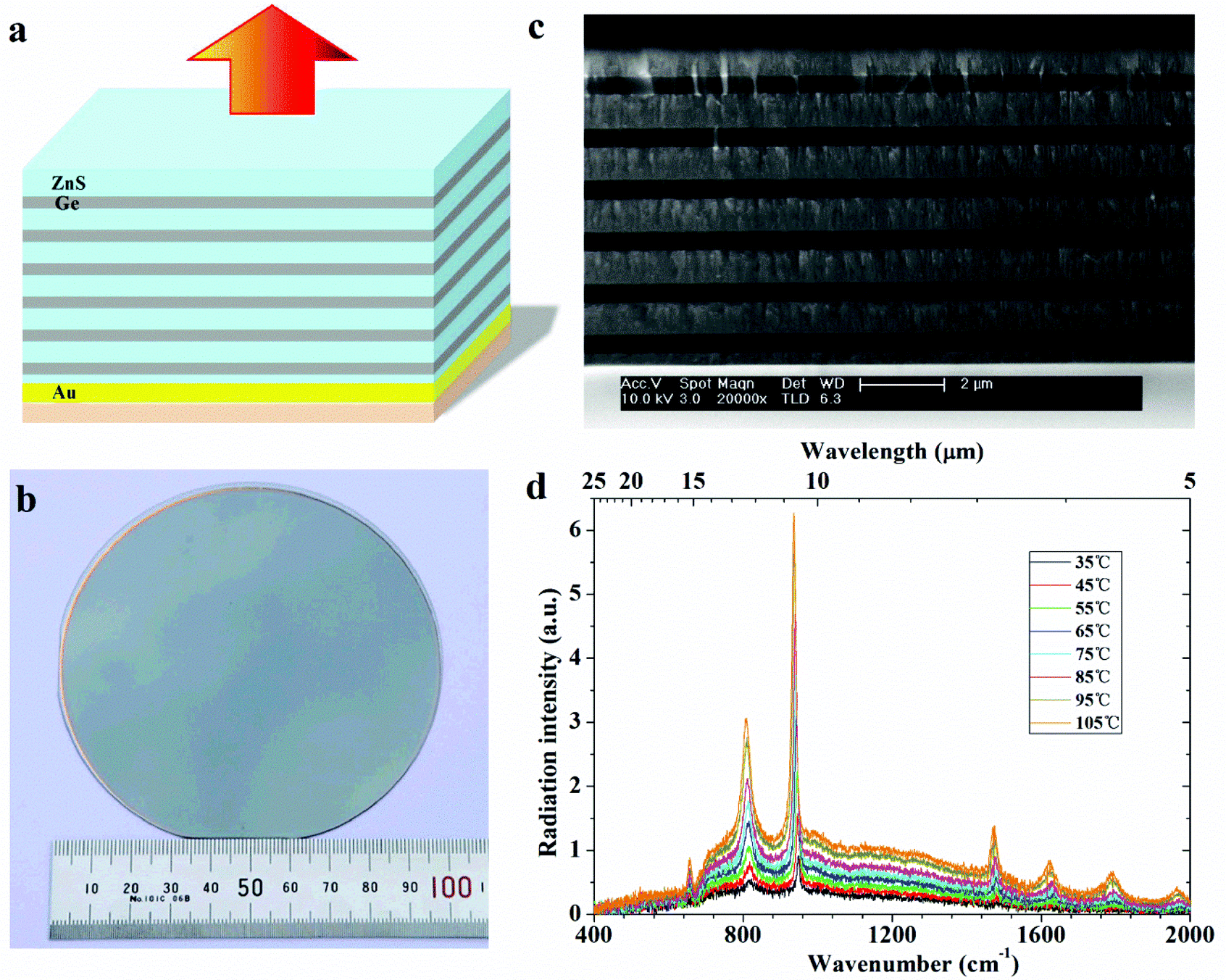 | ||
| Fig. 1 Large-area, narrow-band thermal emitter. (a) Schematic view of the thermal emitter, which consists of a one-dimensional photonic crystal (1DPC) slab, a dielectric spacer and a continuous metallic film. (b) Photograph of a fabricated large-area thermal emitter with diameter of 100 mm (4 inches), where the 1DPC consists of six alternating layers (N = 6) of infrared optical materials (Ge) and zinc sulfide (ZnS) with thickness of 520 nm and 945 nm, respectively. The dielectric spacer and the bottom layer are a 298 nm thick ZnS and a 200 nm thick gold film, respectively. (c) SEM image of part of the fabricated sample. (d) Experimentally measured emission spectra in the normal direction for eight different temperatures. The thermal emitter exhibits a narrow-band thermal emission peak at the wavenumber of 943.4 cm−1. | ||
For the emission studies, the device was mounted on an external heater fed with DC current for heating, and the temperature was monitored using a thermocouple attached to the back side of the sample. Thermal emission spectra were measured using a Fourier-transform infrared (FTIR) spectrometer with a liquid nitrogen-cooled HgCdTe (MCT) detector. Fig. 1d shows the measured emission spectra in the normal direction at eight different temperatures, from 35 °C to 105 °C, in steps of 10 degrees. The detector is not calibrated, and the detection is sensitive to wavelength; hence, the measured results shown in Fig. 1d are expressed in arbitrary units. As can be observed, our device exhibits a narrowband thermal emission peak at the wavenumber of 943.4 cm−1 with the bandwidth of 12.5 cm−1, which can be considered as one of the narrowest bandwidths reported to date. To evaluate the absolute emittance value of the fabricated device, the thermal emission spectrum of a blackbody control sample, a carbon nanotube array, was characterized under the same condition (see Fig. S1a, ESI†). The emission spectrum of the device can thus be normalized by division with the spectrum of the blackbody control sample. It is found that the normalized emittance (referred to as emittance hereinafter) of our device has a peak value of 92% (see Fig. S1b, ESI†).
The spectral-directional emission properties of the thermal emitter were also characterized by tilting the sample at angles of up to 65° to the surface-normal direction. The emittance (measured at the temperature 50 °C) as a function of the wavelength and emission angle for s, p and unpolarized light is presented in Fig. 2a, b and c, respectively. As one can see, the emittance peak positions are dependent on the emission direction and undergo blueshifts for both s and p polarizations as the emission angle increases. Taking s (p) polarization as an example, the corresponding emission peak wavelengths for emission angles of 0°, 25° and 50° are 946.1 cm−1 (946.1 cm−1), 953.3 cm−1 (964.3 cm−1) and 968.9 cm−1 (1003.1 cm−1), respectively. This result elucidates that for a given radiation wavelength, the emitted light should be directed into a well-defined angular region.
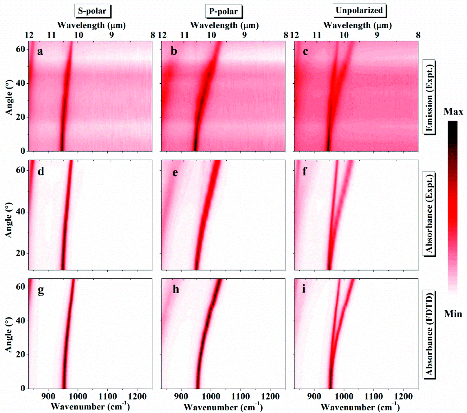 | ||
| Fig. 2 Spectral-directional emission and absorption properties of the thermal emitter. (a)–(c) Experimentally measured emittance as a function of the wavelength and emission angle for s, p and unpolarized light, respectively. Note that the emittance peak positions are dependent on the emission direction and undergo blueshifts as the emission angle increases. (d)–(f) Experimental measured absorbance as a function of the wavelength and incident angle (due to the limitation of variable angle reflection accessory, the minimum allowable incident angle is 13°) for s, p and unpolarized light, respectively. (g)–(i) The corresponding theoretical absorbance spectra for the three cases. Both experimental and theoretical absorbance data are found to be in good accordance with the thermal emittance spectra. | ||
To investigate the angular response of the emission pattern and the level of directionality, a three-dimensional (3D) image of the angular distribution of emission at the above three emission peak wavelengths for s polarization is plotted in Fig. 3a. As expected, for the wavenumber of 946.1 cm−1, the emission of the thermal emitter is concentrated in a narrow beam around the normal orientation of the structure, with a solid angle of 0.325 sr. For the wavenumbers of 953.3 cm−1 and 968.9 cm−1, the emission is respectively confined in the lobes centered at 25° and 50°, with half-power angular widths of 24.5° and 11.5°. The angular distribution of the emission pattern for p polarization is displayed in Fig. 3b, which exhibits similar behavior to s polarization but with greater concentration at the corresponding emission angles (details of this case are presented in the figure caption). More interestingly, for both polarizations, due to the nature of the planar structure, the angular emission pattern of our emitter has circular symmetry and resembles a blooming Calystegia flower. This feature is in great contrast to that of optical antennas.39,40 All of these experiments show unambiguous evidence of an extremely large-area, lithography-free, narrow-band thermal emitter, and highlight its potential function as a highly directional mid-infrared light source.
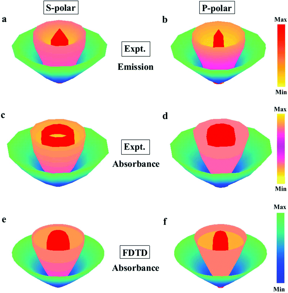 | ||
| Fig. 3 Angular responses of the emission and absorbance patterns of the thermal emitter. (a), (b) Angular distributions of emissions at three emission peak wavenumbers for s and p polarization, respectively. For s (p) polarization, at 946.1 cm−1, the emission of the thermal emitter is concentrated in a narrow beam around the normal direction (denoted by autumn colormap) of the structure with a solid angle of 0.325 sr (0.115 sr), while at 953.3 cm−1 (964.3 cm−1) and 968.9 cm−1 (1003.1 cm−1), the emissions are respectively confined in the lobes centered at 25° (denoted by spring colormap) and 50° (denoted by winter colormap), with half-power angular widths of 24.5° (18.75°) and 11.5° (11°). (c), (d) Angular distributions of experimental absorbance at the given radiation wavelengths for both s and p polarizations, respectively. Due to the limitation of the variable angle reflection accessory, the minimum allowable incident angle is 13°. (e), (f) The corresponding angular distributions of theoretical absorbance for the two polarizations. | ||
The radiative properties of the proposed thermal emitter are governed by Kirchhoff's Law. Since there is an optically thick gold film as ground plane to prevent light transmission, the angular and frequency-dependent emittance E(ω, θ) can be simply expressed as E(ω, θ) = A(ω, θ) = 1 − R(ω, θ), where A is the absorbance and R is the reflectance of the thermal emitter. In order to confirm our experimental observation and demonstrate the applicability of the above formula while reducing the issue of emission to the study of the absorption/reflection, additional optical measurements and analytical calculations were performed. Fig. 2d–f displays the experimental absorbance (obtained based on the experimental reflectance measured at room temperature) as a function of the wavenumber and incident angle for s, p and unpolarized light, respectively. Due to the limitation of the variable angle reflection accessory, the minimum allowable incident angle is 13°. The corresponding theoretical absorbance spectra for the three cases are presented in Fig. 2g–i. Numerical simulations in our study are based on the finite-difference-time-domain (FDTD) method. The structure parameters used are the same as the fabricated sample. Both experimental and theoretical absorbance data are found to be in good accordance with the thermal emittance spectra. Angle dependencies of the absorbance at the given radiation wavelengths for both s and p polarizations were also experimentally and theoretically evaluated, and depicted in Fig. 3c and d. These results not only confirm that such a thermal emitter radiates infrared light in well-defined directions, but also verify the validity of Kirchhoff's law indicating that developing a specific functional thermal emitter is equivalent to the design of an absorber with similar characteristics.
It should be pointed out that although the agreement among the experimental and theoretical results as shown in Fig. 2 and 3 is fairly good, there are several discrepancies. For visual clarity, we plot the theoretical reflection and absorption spectra at normal incidence in Fig. 4a and the corresponding experimental results at the incident angle of 13° in Fig. 4b, and show an enlarged view of the measured emission spectra for six different temperatures at normal incidence in Fig. 4c. As one can see that: (i) the peak values of experimental absorbance (93%, with a bandwidth of 8.8 cm−1) and emittance are a little less than the theoretical value, which as predicted, can be as high as ∼100%, while their bandwidths are larger than the theoretical value of 7.7 cm−1 (corresponding to a quality Q factor, Q = ωres/Δωres, with ωres as the resonance frequency and Δωres as the line width, of 124). We infer that this deviation mainly results from the imperfections of the multilayered structure, including random thickness fluctuations and the diffusive intermixing at the interfaces.41,42 (ii) Compared with the experimental and theoretical absorbance spectra (obtained at room temperature), the experimental thermal emission peak slightly shifts to long wavelengths as the operating temperature increases. The reason for this issue is predominantly attributed to the temperature dependence of the material's refractive index, rather than the thermal expansion effect24 (see ESI Note 1 and Fig. S2† for more details).
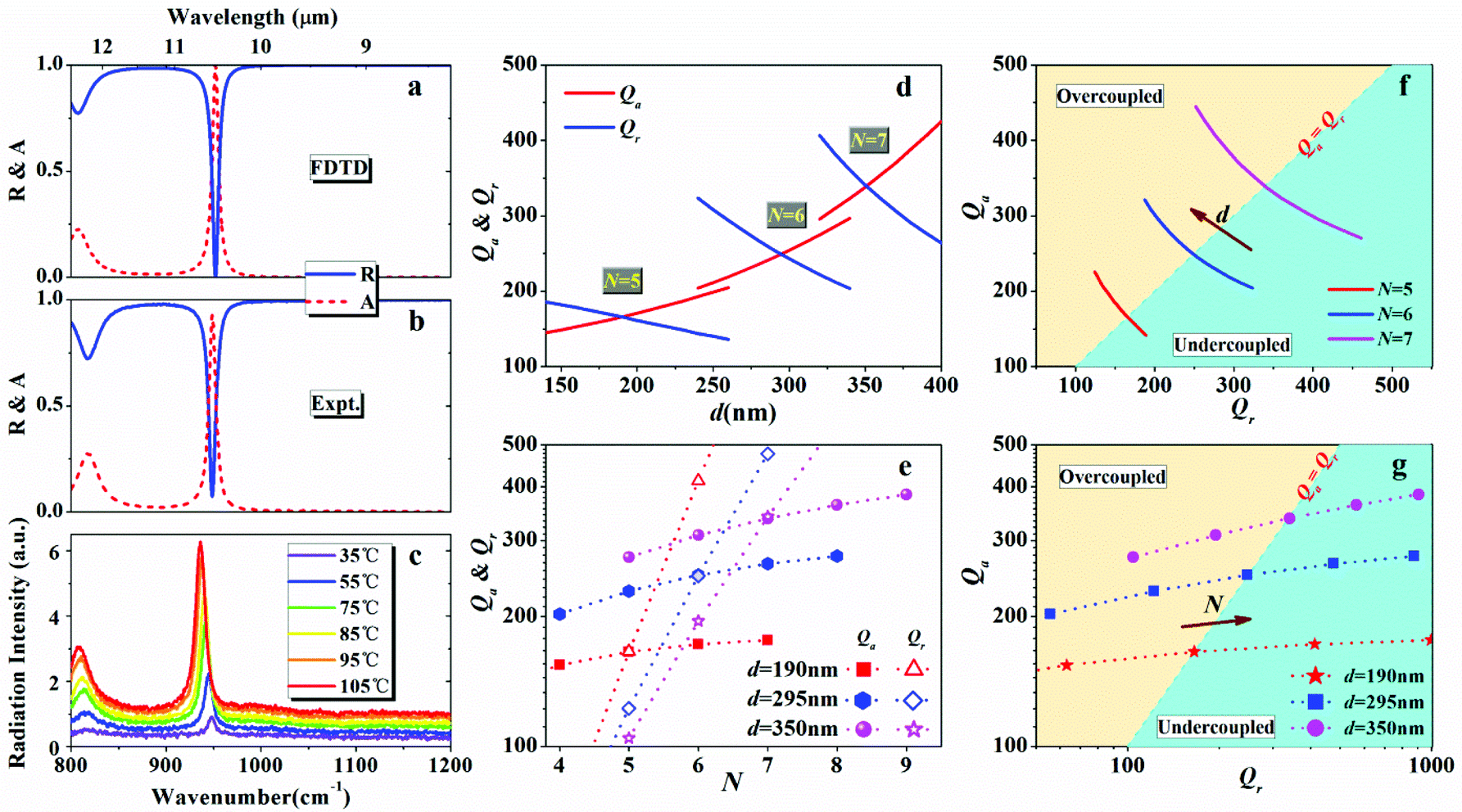 | ||
| Fig. 4 Reflection, absorption, and emission spectra of the thermal emitter at normal incidence and a general theoretical guidance for narrowband thermal emitter design. (a) Theoretical reflectance and absorbance spectra of our thermal emitter at normal incidence. (b) Experimental reflectance and absorbance spectra of the thermal emitter at 13° angle of incidence. (c) Enlarged view of the measured emission spectra for six different temperatures. (d) Qa and Qr as functions of the thickness of dielectric spacer d for the thermal emitters with three different numbers of photonic crystal periods. (e) Qa and Qr as functions of the number of photonic crystal periods N for the thermal emitters with three different thicknesses of dielectric spacer. (f), (g) Replot of the results shown in (d) and (e) into a Qa − Qr diagram. Note that the Q factors can be tuned from overcoupled to undercoupled region and to match the critical coupling condition (Qa = Qr) by adjusting the geometric parameter. | ||
On closer inspection of our thermal emitter, it turns out that this device can be regarded as a resonant cavity (dielectric spacer) surrounded on both sides by two optical mirrors. The top truncated 1DPC has photonic bandgaps for both s and p polarizations, as shown in Fig. 5a (light yellow regions), over which it blocks light, thus acting as a partially reflective dielectric mirror. The bottom gold layer not only functions as a metallic cavity mirror but, more importantly, serves as the source of thermal radiation, as both the dielectric spacer and the 1DPC are lossless. Such a multilayered heterostructure supports a surface-wave-like resonant mode (solid symbols in Fig. 5a) within the photonic bandgap, which can be directly coupled to propagating waves in free space.43 The observed enhanced thermal emission is strongly linked to the enhancement of the optical mode density and has a similar origin as the cavity quantum electrodynamics (QED) Purcell effect.20,44,45
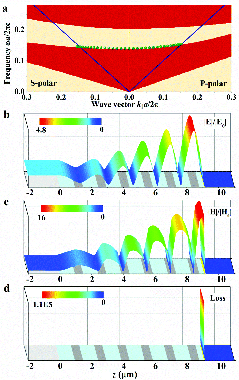 | ||
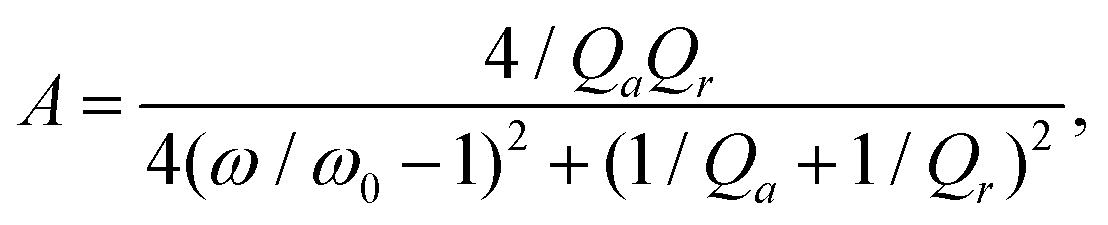
| Fig. 5 Projected band structure and electromagnetic field distributions. (a) Projected band structure of the 1D photonic crystal with the light line (solid line) and resonant cavity modes (solid symbols). The allowed and forbidden modes are indicated by red and light yellow regions, respectively. (b), (c) The normalized electric and magnetic field amplitudes at the absorption peak wavenumber of 952.4 cm−1, respectively. The calculated electric and magnetic fields are strongly enhanced inside the cavity layer and exhibit exponentially oscillating decay toward the opposite direction of z axis, showing effective surface wave behavior. (d) The time-averaged power dissipation density (W m−2) for the same case. The calculated results show that the energy of incident light is only completely dissipated by the bottom gold layer. | ||
In order to illustrate the nature of resonant enhancement of the thermal emission, we investigated the electromagnetic field distribution inside the structure, as it is excited by a normally incident plane wave. Fig. 5b and c show the normalized electric and magnetic field amplitudes at the absorption peak wavenumber of 952.4 cm−1. As can be observed, the calculated electric and magnetic fields are strongly enhanced inside the cavity layer and exhibit exponentially oscillating decay toward the opposite direction of z axis, revealing effective surface wave behavior. To provide further theoretical insights, the time-averaged power dissipation density (W m−2) was investigated for the same case and is plotted in Fig. 5d. In the calculations, the temperature dependence of material properties has been neglected. The calculated results show that the energy of incident light is completely dissipated by the bottom gold layer only, indicating that this gold layer is really acting both as the cavity mirror and the thermal radiation source.34
Finally, in order to show how to develop an optimized device design for fabrication, we investigated the absorption/emission properties of the thermal emitter using CMT combined with transfer-matrix approach. For the emitter constructed by one-dimensional multilayered resonant structure, owing to the presence of the bottom gold layer, no light energy can pass through it, so that it can be well described by a one-port single-mode resonator model according to the CMT. The absorbance of such model can be expressed as32,46
 | (1) |
Conclusions
In short, we have experimentally and theoretically demonstrated a large-area, lithography-free, narrow-band and highly directional mid-infrared thermal emitter. Experimental results show that our emitter exhibits a narrowband thermal emission peak at the wavenumber of 943.4 cm−1 with thermal emission efficiency (power emitted within the wavelength range of interest divided by total thermal power emitted at all frequencies in the normal direction) of 5.9% at the temperature of 105 °C. The experimental emittance spectra are found to be in good agreement with the experimental and calculated absorption spectra. Although Fig. 5a notes that the resonant mode is located in the vicinity of the band edge,15,16 it does not mean that the condition of band edge resonance is necessary for this type of thermal emitter. High emittance can be obtained and tuned to other positions by rearranging the location of the cavity layer (see Fig. S4, ESI†) or using other aperiodic multilayered structures.38,49,50 To illustrate the functionality of the device, a thermal infrared emission image of a designed pattern based on the thermal emitter was taken and is presented in Fig. S5 (ESI†). We believe that the proposed thermal emitter can be implemented for further applications, such as infrared sensing, medical systems, etc.Experimental section
Sample fabrication
A double-polished silicon substrate was cleaned by acetone, alcohol and DI water with ultrasonication in turn, then dried with nitrogen gas. A 200 nm thick gold (Au) film was deposited on the substrate by using a deposition system (MANTIS Deposition Ltd Qprep series). The deposition power was 100 W, and thickness was controlled by a quartz crystal oscillator. An ultrathin layer of chromium (Cr) was inserted between the substrate and Au film to enhance the adhesion. Then, the gold-coated substrate was placed into the chamber of a Leybold advanced optical deposition system (ARES1100) to deposit the ZnS and Ge films. The materials used were 99.99% purity for ZnS and Ge. The vacuum was 8 × 10⁻⁴ Pa, and deposition temperature was 150 °C. The evaporation rates of ZnS and Ge films were controlled by the PID control system, and their thicknesses were precisely controlled by the optical monitor OMS5000. A 298 nm thick ZnS layer was deposited firstly on the Au film as cavity. Then, six layers of Ge and ZnS were deposited alternately to form the photonic crystal structure, with thicknesses of 520 nm and 945 nm, respectively. The morphology of the fabricated sample was characterized using a scanning electron microscope (SEM, FEI Sirion 200) operating at an accelerating voltage of 10 kV.Optical characterizations
The angular polarized emission spectra of the infrared narrowband emitter sample were recorded using a Fourier transform infrared spectrometer (Bruker IFS 125HR). The sample was fixed on a homemade pillar holder, which could be heated and rotated to measure the emission spectra at different angles (see ESI Fig. S6 and S7†). The narrowband emitter we fabricated acted as the light source of the spectrometer during measurement. A mid-infrared polarizer (KRS-5) was placed in the sample chamber of the spectrometer to obtain both s and p polarization spectra. The angle-resolved reflectance (absorbance) spectra measurements were performed using the same FTIR system, which was equipped with a reflection module allowing for angles ranging 13°–85°. The measured reflection spectra were normalized with respect to a gold mirror. A KRS-5 infrared polarizer was placed in the light path to obtain the spectra for different polarization states.Numerical simulations
Full-wave numerical simulations were performed using the commercial package Lumerical FDTD Solutions, based on FDTD method. In our simulations, the dielectric permittivity of gold is taken from ref. 51. The refractive indices of Ge and ZnS are respectively assumed to be constant, 4.166 and 2.242, within the region of interest. Transmission and reflection were respectively collected with power monitors behind the incident wave and the structure. Two-dimensional field profile monitors were utilized to record electromagnetic field distributions.Author contributions
X. L., Z. L., Z. W. and M. W. contributed equally to this work and are joint first authors. X. L. carried out the sample fabrication. Z. L. performed the simulations. Z. W. conducted the theoretical analysis. M. W. and J. L. performed the thermal emission measurements. X. C. and X. Z. assisted with the sample fabrication. B. Z. built the experimental set-up. R. J., Y. Z, and L. S. assisted with the optical measurements. J. H. and S. W. directed the research. J. H. wrote the manuscript. All authors discussed the results and commented on the manuscript.Conflicts of interest
The authors declare no competing financial and nonfinancial interests.Acknowledgements
This work is supported by National Key R&D Program of China (2017YFA0205800), National Natural Science Foundation of China (61471345, 11874376, 11604355, 61705127), the National Young 1000 Talent Plan, and Shanghai Science and Technology Committee (18590712600, 16JC1403500, 19DZ2293400, 18DZ2282200, 19ZR1465900).References
- Y. Gong, Z. Wang, K. Li, L. Uggalla, J. Huang, N. Copner, Y. Zhou, D. Qiao and J. Zhu, Opt. Lett., 2017, 42, 4537–4540 CrossRef CAS PubMed.
- P. Werle, F. Slemr, K. Maurer, R. Kormann, R. Mücke and B. Jänker, Opt. Lasers Eng., 2002, 37, 101–114 CrossRef.
- H. N. Li, D. S. Li and G. B. Song, Eng. Struct., 2004, 26, 1647–1657 CrossRef.
- E. Rephaeli and S. Fan, Opt. Express, 2009, 17, 15145–15159 CrossRef CAS PubMed.
- A. Lenert, D. M. Bierman, Y. Nam, W. R. Chan, I. Celanović, M. Soljačić and E. N. Wang, Nat. Nanotechnol., 2014, 9, 126–130 CrossRef CAS PubMed.
- J. Hodgkinson and R. P. Tatam, Meas. Sci. Technol., 2013, 24, 012004 CrossRef.
- T. Wang, P. Li, D. N. Chigrin, A. J. Giles, F. J. Bezares, O. J. Glembocki, J. D. Caldwell and T. Taubner, ACS Photonics, 2017, 4, 1753–1760 CrossRef CAS.
- N. Gaponik, I. L. Radtchenko, M. R. Gerstenberger, Y. A. Fedutik, G. B. Sukhorukov and A. L. Rogach, Nano Lett., 2003, 3, 369–372 CrossRef CAS.
- X. Liu, T. Starr, A. F. Starr and W. J. Padilla, Phys. Rev. Lett., 2010, 104, 207403 CrossRef PubMed.
- W. Li, Y. Shi, Z. Chen and S. Fan, Nat. Commun., 2018, 9, 4240 CrossRef PubMed.
- Y. Li, X. Bai, T. Yang, H. Luo and C. W. Qiu, Nat. Commun., 2018, 9, 273 CrossRef PubMed.
- A. A. Bergh and P. J. Dean, Proc. IEEE, 1972, 60, 156–223 Search PubMed.
- D. Delbeke, R. Bockstaele, P. Bienstman, R. Baets and H. Benisty, IEEE J. Sel. Top. Quantum Electron., 2002, 8, 189–206 CrossRef CAS.
- J. Faist, F. Capasso, D. L. Sivco, C. Sirtori, A. L. Hutchinson and A. Y. Cho, Science, 1994, 264, 553–556 CrossRef CAS PubMed.
- M. U. Pralle, N. Moelders, M. P. McNeal, I. Puscasu, A. C. Greenwald, J. T. Daly, E. A. Johnson, T. George, D. S. Choi, I. El-Kady and R. Biswas, Appl. Phys. Lett., 2002, 81, 4685–4687 CrossRef CAS.
- M. De Zoysa, T. Asano, K. Mochizuki, A. Oskooi, T. Inoue and S. Noda, Nat. Photonics, 2012, 6, 535–539 CrossRef CAS.
- D. D. Kang, T. Inoue, T. Asano and S. Noda, Appl. Phys. Lett., 2017, 110, 181109 CrossRef.
- D. D. Kang, T. Inoue, T. Asano and S. Noda, ACS Photonics, 2019, 6, 1565–1571 CrossRef CAS.
- S. Maruyama, T. Kashiwa, H. Yugami and M. Esashi, Appl. Phys. Lett., 2001, 79, 1393 CrossRef CAS.
- K. J. Vahala, Nature, 2003, 424, 839–846 CrossRef CAS PubMed.
- J. J. Greffet, R. Carminati, K. Joulain, J. P. Mulet, S. Mainguy and Y. Chen, Nature, 2002, 416, 61–64 CrossRef CAS PubMed.
- M. W. Tsai, T. H. Chuang, C. Y. Meng, Y. T. Chang and S. C. Lee, Appl. Phys. Lett., 2006, 89, 173116 CrossRef.
- C.-M. Wang, Y.-C. Chang, M.-W. Tsai, Y.-H. Ye, C.-Y. Chen, Y.-W. Jiang, Y.-T. Chang, S.-C. Lee and D. P. Tsai, Opt. Express, 2007, 15, 14673–14678 CrossRef PubMed.
- X. Liu, T. Tyler, T. Starr, A. F. Starr, N. M. Jokerst and W. J. Padilla, Phys. Rev. Lett., 2011, 107, 45901 CrossRef PubMed.
- D. Costantini, A. Lefebvre, A. L. Coutrot, I. Moldovan-Doyen, J. P. Hugonin, S. Boutami, F. Marquier, H. Benisty and J. J. Greffet, Phys. Rev. Appl., 2015, 4, 014023 CrossRef.
- T. Yokoyama, T. D. Dao, K. Chen, S. Ishii, R. P. Sugavaneshwar, M. Kitajima and T. Nagao, Adv. Opt. Mater., 2016, 4, 1987–1992 CrossRef CAS.
- J. A. Schuller, T. Taubner and M. L. Brongersma, Nat. Photonics, 2009, 3, 658–661 CrossRef CAS.
- T. Inoue, M. De Zoysa, T. Asano and S. Noda, Optica, 2015, 2, 27–35 CrossRef CAS.
- J.-J. Greffet and M. Nieto-Vesperinas, J. Opt. Soc. Am. A, 1998, 15, 2735 CrossRef.
- H. A. Haus, Waves and Fields in Optoelectronics, Prentice-Hall, Englewood Cliffs, NJ, 1984 Search PubMed.
- S. Fan, W. Suh and J. D. Joannopoulos, J. Opt. Soc. Am. A, 2003, 20, 569–572 CrossRef PubMed.
- C. Qu, S. Ma, J. Hao, M. Qiu, X. Li, S. Xiao, Z. Miao, N. Dai, Q. He, S. Sun and L. Zhou, Phys. Rev. Lett., 2015, 115, 235503 CrossRef PubMed.
- P. Yeh, Optical Wave in Layered Media, Wiley, New York, 1988 Search PubMed.
- I. Celanovic, D. Perreault and J. Kassakian, Phys. Rev. B: Condens. Matter Mater. Phys., 2005, 72, 75127 CrossRef.
- B. J. Lee, C. J. Fu and Z. M. Zhang, Appl. Phys. Lett., 2005, 87, 071904 CrossRef.
- Z. Y. Yang, S. Ishii, T. Yokoyama, T. D. Dao, M. G. Sun, P. S. Pankin, I. V. Timofeev, T. Nagao and K. P. Chen, ACS Photonics, 2017, 4, 2212–2219 CrossRef CAS.
- Z. Wang, J. K. Clark, Y. L. Ho, B. Vilquin, H. Daiguji and J. J. Delaunay, ACS Photonics, 2018, 5, 2446–2452 CrossRef CAS.
- A. Sakurai, K. Yada, T. Simomura, S. Ju, M. Kashiwagi, H. Okada, T. Nagao, K. Tsuda and J. Shiomi, ACS Cent. Sci., 2019, 5, 319–326 CrossRef CAS PubMed.
- T. Kosako, Y. Kadoya and H. F. Hofmann, Nat. Photonics, 2010, 4, 312–315 CrossRef CAS.
- L. Novotny and N. Van Hulst, Nat. Photonics, 2011, 5, 83–90 CrossRef CAS.
- M. T. Asom, M. Geva, R. E. Leibenguth and S. N. G. Chu, Appl. Phys. Lett., 1991, 59, 976–978 CrossRef CAS.
- Ž. Gačević and N. Vukmirović, Phys. Rev. Appl., 2018, 9, 64041 CrossRef.
- B. J. Lee and Z. M. Zhang, J. Heat Transfer, 2007, 129, 17 CrossRef CAS.
- E. M. Purcell, Phys. Rev., 1946, 69, 681 CrossRef.
- L. Novotny and B. Hecht, Principles of Nano-Optics, Cambridge University Press, 2006 Search PubMed.
- T. Inoue, M. De Zoysa, T. Asano and S. Noda, Phys. Rev. B: Condens. Matter Mater. Phys., 2015, 91, 235316 CrossRef.
- D. L. C. Chan, I. Celanovic, J. D. Joannopoulos and M. Soljačić, Phys. Rev. A, 2006, 74, 064901 CrossRef.
- M. Ghebrebrhan, P. Bermel, Y. X. Yeng, I. Celanovic, M. Soljačić and J. D. Joannopoulos, Phys. Rev. A, 2011, 83, 33810 CrossRef.
- C. H. Granier, F. O. Afzal, C. Min, J. P. Dowling and G. Veronis, J. Opt. Soc. Am. B, 2014, 31, 1316–1321 CrossRef CAS.
- J. Drevillon and P. Ben-abdallah, J. Appl. Phys., 2007, 102, 114305 CrossRef.
- E. D. Palik, Handbook of Optical Constants of Solids, Academic Press, 1985 Search PubMed.
Footnotes |
| † Electronic supplementary information (ESI) available: Details of the temperature-dependent absorption/emission properties of the thermal emitter, analytical relationships between Q factors and the geometrical parameters, retrieving Q factors based on experimental and numerical simulation results, etc. See DOI: 10.1039/c9nr06181a |
| ‡ These authors contributed equally to this work. |
| This journal is © The Royal Society of Chemistry 2019 |