
Gradient oxygen doping triggered a microscale built-in electric field in CdIn2S4 for photoelectrochemical water splitting†
Jingwen
Sun‡
 *,
Shangling
Han‡
,
Fanglei
Yao
,
Ruixin
Li
,
Chenchen
Fang
,
Xiaoyuan
Zhang
,
Yaya
Wang
,
Xuefeng
Xu
,
Di
Wu
,
Kai
Liu
,
Pan
Xiong
and
Junwu
Zhu
*,
Shangling
Han‡
,
Fanglei
Yao
,
Ruixin
Li
,
Chenchen
Fang
,
Xiaoyuan
Zhang
,
Yaya
Wang
,
Xuefeng
Xu
,
Di
Wu
,
Kai
Liu
,
Pan
Xiong
and
Junwu
Zhu
Key Laboratory for Soft Chemistry and Functional Materials, Ministry of Education, Nanjing University of Science and Technology, Nanjing 210094, China. E-mail: Jingwen_Sun@njust.edu.cn
First published on 24th January 2024
Abstract
Construction of a built-in electric field has been identified as an attractive improvement strategy for photoelectrochemical (PEC) water splitting by facilitating the carrier extraction from the inside to the surface. However, the promotion effect of the electric field is still restrained by the confined built-in area. Herein, we construct a microscale built-in electric field via gradient oxygen doping. The octahedral configuration of the synthesized CdIn2S4 (CIS) provides a structural basis, which enables the subsequent oxygen doping to reach a depth of ∼100 nm. Accordingly, the oxygen-doped CIS (OCIS) photoanode exhibits a microscale built-in electric field with band bending. Excellent PEC catalytic activity with a photocurrent density of 3.69 mA cm−2 at 1.23 V vs. RHE is achieved by OCIS, which is 3.1 times higher than that of CIS. Combining the results of thorough characterization and theoretical calculations, accelerating migration and separation of charge carriers have been determined as the reasons for the improvement. Meanwhile, the recombination risk at the doping centers has also been reduced to the minimum via optimal experiments. This work provides a new-generation idea for constructing a built-in electric field from the view point of bulky configuration towards PEC water splitting.
 Jingwen Sun | Dr Jingwen Sun is an associate professor at Nanjing University of Science and Technology, China. She received her PhD in materials science and engineering from the same university in 2016. She was a visiting PhD student at Max Planck Institute of Colloids and Interfaces in Germany, followed by a postdoctoral researcher at Ben-Gurion University of the Negev, Israel. Her research focuses on the rational design of nitrides and carbides towards energy conversion and storage applications. |
Introduction
Photoelectrochemical (PEC) water splitting is regarded as a promising strategy for addressing the energy crisis and environmental challenges1–5 Rational design of photoanodes with high photoelectric activity is of great importance to achieve the ideal conversional efficient.6,7 Most of the reported photoanodes in PEC cells are based on metal oxides, including WO3,8 ZnO,9 In2O3,10 Fe2O3![[thin space (1/6-em)]](https://www.rsc.org/images/entities/char_2009.gif) 11,12 and BiVO4,13etc. However, the valence band (VB) is occupied by the O-2p orbital, resulting in an expanded bandgap and limiting its response to only UV light.14,15 The limitation is unfavorable for efficiently harnessing light energy.16,17 In contrast, metal sulfides demonstrate enhanced utilization of solar light owing to their narrower bandgaps,18,19 such as CdS,20 ZnS,21 SnS2,22 ZnIn2S4,23 and CdIn2S4,24 especially the latest ternary sulfides. In brief, the S-3p orbital occupies the VB position in metal sulfides, positioned higher than the O-2p orbital, resulting in the formation of a more negative VB and faster hole mobility.25–27 Nevertheless, the low photoinduced carrier separation efficiency and slow oxygen evolution reaction (OER) kinetics still impede the application of ternary sulfides in the PEC field.28–30 Therefore, there is a strong desire to develop efficient approaches to solve these drawbacks.
11,12 and BiVO4,13etc. However, the valence band (VB) is occupied by the O-2p orbital, resulting in an expanded bandgap and limiting its response to only UV light.14,15 The limitation is unfavorable for efficiently harnessing light energy.16,17 In contrast, metal sulfides demonstrate enhanced utilization of solar light owing to their narrower bandgaps,18,19 such as CdS,20 ZnS,21 SnS2,22 ZnIn2S4,23 and CdIn2S4,24 especially the latest ternary sulfides. In brief, the S-3p orbital occupies the VB position in metal sulfides, positioned higher than the O-2p orbital, resulting in the formation of a more negative VB and faster hole mobility.25–27 Nevertheless, the low photoinduced carrier separation efficiency and slow oxygen evolution reaction (OER) kinetics still impede the application of ternary sulfides in the PEC field.28–30 Therefore, there is a strong desire to develop efficient approaches to solve these drawbacks.
Constructing a built-in electric field by means of heterojunction engineering, cocatalysts introduction, facet junctions and element doping shows great promise for improving the PEC activity of ternary sulfides via manipulating the migration of photogenerated carriers to spatially separated reductive as well as oxidative sites.31,32 For instance, Meng et al.33 reported a CdIn2S4/In2S3/SnO2 composite, which was synthesized via the aid of Ni–phthalocyanine during the reaction followed by decorating the ultrathin amorphous SnO2 layer. The built-in electric field was constructed during the junction interface, providing the composite with improved surface OER kinetics, accelerated charge transfer, and enhanced catalytic performance. Li et al.34 developed a ZnIn2S4/SnS2 (ZIS-O-TS) composite via a combined strategy of hydrothermal method and water bath reaction. Band adaptation of the ZIS-O-TS was achieved through the new chemical bonds between the components. The established built-in electric field promoted the carrier separation and migration. However, as known from the reported literature, the depth of the built-in electric field near to heterocontacts is limited to only a few tens of nanometers.35 Beyond this range, photoexcited carriers still exhibit severe recombination.36 Therefore, reducing the recombination of carriers outside the electric field remains a critical issue for further enhancing the PEC activity of ternary sulfides.
Recently, gradient elemental doping has emerged as a candidate approach for expanding the range of the built-in electric field.9,37 Gradient oxygen doping from the surface to the bulk will generate intermediate states, therefore resulting in a reduced bandgap along with an enhanced light absorption capacity. Moreover, the VB bending, constructed from the gradient oxygen doping, may construct a microscale built-in electric field, thereby suppressing the bulky carrier recombination. However, in spite of the positive effect, excessive dopants in the photocatalyst may hinder the further improvement of the PEC activity by serving as carrier recombination centers.38,39 Therefore, regulating the dopants to an appropriate concentration is quite important for improving the PEC performance. More importantly, recent doping strategies have mostly focused on the 2D materials for their high specific surface area, and bulky morphologies have received less research interest.18
To this end, octahedral CdIn2S4 (CIS) is synthesized and selected as a typical bulky ternary sulfide. The relevant thicker morphology provides a structural basis for deeper elemental doping, allowing the creation of a wide-range built-in electric field. Further derived from the optimal annealing strategy, CIS with gradient oxygen doping (OCIS) has been successfully constructed. A continuous band bending is established by the analysis of UV-visible diffuse reflectance spectra and X-ray photoelectron spectra, thus endowing the realization of a microscale built-in electric field. Attributed to the improvement of carrier separation and migration, the optimal OCIS demonstrates a photocurrent density of 3.69 mA cm−2 at 1.23 V vs. RHE, which is 3.1 times higher than that of CIS.
Experimental
Chemicals
Cadmium nitrate hydrate (Cd(NO3)2·4H2O), indium hydrate (In(NO3)3·xH2O), thiourea (CH4N2S), sodium sulfate anhydrous (Na2SO4), and sodium sulfite anhydrous (Na2SO3) were purchased from Shanghai Aladdin Bio-Chem Technology Co., Ltd. Sodium sulfide hydrate (Na2S·9H2O) was purchased from Shanghai Macklin Biochemical Co., Ltd.Synthesis of the CdIn2S4 (CIS) photoanode
The preparation of the CIS photoanode involved a straightforward hydrothermal method. The precursor solution was created by adding Cd(NO3)2·5H2O (0.25 mmol), In(NO3)3·xH2O (0.50 mmol) and CH3N2S (1.00 mmol) to 25 mL of ultra-pure water. The fluorine-doped tin oxide conductive (FTO) glass underwent a pretreatment process involving sequential sonication in acetone, ethanol, and ultra-pure water. Afterwards, the cleaned FTO glass was positioned within the autoclave. The autoclave was then closed and reacted at 200 °C for 5 h. Next, the resulting product was washed with absolute ethanol and ultra-pure water. Finally, it was dried under vacuum.Synthesis of the O doped CdIn2S4 (OCIS) photoanode
In a standard procedure, the synthesized CIS photoanode was subjected to annealing for 2 h under an air atmosphere at the temperature of 300 °C. After cooling naturally, the product was labelled as OCIS. For comparison, the annealing temperature (100, 200, 400, 500 °C) and duration (1, 3, 4 h) were further optimized.Characterization
The X-ray diffraction (XRD) patterns of the materials were obtained using a Bruker D8 Advance diffractometer (40 kV, 40 mA, Cu Kα radiation, λ = 1.5418 Å). X-ray photoelectron spectra (XPS) were acquired with a PHI QUANTERA II X-ray photoelectron spectroscope. Monochromatic Al Kα radiation was employed as the excitation source (energy resolution <0.60 eV). The binding energy (BE) values were calibrated using the C (1 s) peak (284.8 eV). The Raman spectra were obtained using an inVia confocal Raman microscope (Renishaw). Fourier-transform infrared spectroscopy (FTIR) was measured using a Thermo Fisher Scientific NICOLET IS10 spectrometer. The morphology of the materials was imaged using a scanning electron microscope (SEM, JEOL JSM-7001F) and a transmission electron microscope (TEM, JEOL JEM-2100). The photoluminescence (PL) spectra (excited by 325 nm illumination) were record on an FLS1000 (Edinburgh Instruments), in which the excitation pulse comes from a 325-W Xe lamp. The time-resolved transient photoluminescence (TRPL) spectra were recorded on an FLS1000 (Edinburgh Instruments) using a 375 nm laser with pulse width of 81.9 ps. UV-visible diffuse reflectance spectra (DRS) were measured using a SHIMADZU UV-2550 spectrophotometer equipped with an integrating sphere. Gas production was measured by gas chromatography (GC9720Plus, Fuli Instruments). The photocatalytic H2 evolution activity was measured using an all-glass automatic online trace gas analysis system (Labsolar-6A, Beijing Perfectlight).PEC measurements
The PEC performance was evaluated on an electrochemical workstation (VersaSTAT3). Ag/AgCl and platinum sheet (1 cm × 2 cm) were used as the reference and counter electrodes, respectively, and the as-prepared photoanodes were used as the working electrode. The PEC water splitting performance was tested in a neutral solution of 0.5 M Na2SO4 (pH = 7), and the PEC sulfite oxidation performance was tested in a mixed solution of 0.35 M Na2SO3 and 0.25 M Na2S (pH = 12.5). The simulated solar light (100 mW cm−2) was provided by a sunlight simulator (XES-50S2) with an AM 1.5G solar simulator filter. The test area is 1 cm2. All PEC tests were irradiated from the back-side of the FTO. Linear sweep voltammetry (LSV) plots were recorded at a scan rate of 20 mV s−1. Electrochemical impedance spectroscopy (EIS) was conducted under illumination at the open-circuit potential (OCP) over the frequency range from 0.1 Hz to 105 Hz with a 10 mV amplitude. Mott–Schottky (M–S) plots were generated in the dark at various alternating current (AC) frequencies of 1, 5, and 9 kHz. The OCP and cyclic voltammograms (CV) were obtained under the same experimental conditions.The measured potential versus Ag/AgCl (EAg/AgCl) was converted to reversible hydrogen electrode (RHE) potential (ERHE) by the Nernst equation:
| ERHE = EAg/AgCl + 0.059 pH + 0.1976 | (1) |
The applied bias photon-to-current efficiency (ABPE) was calculated from the J–V curve using the equation:40
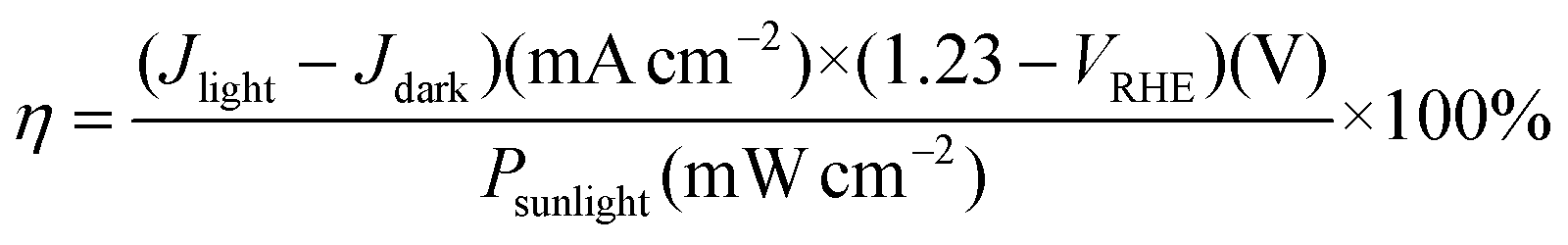 | (2) |
The incident photon-to-current conversion efficiency (IPCE) test was carried out at 0.6 V vs. RHE. A 300-W xenon lamp equipped with a monochromator was used for the monochromatic light irradiation test. The IPCE equation is as follows:40
 | (3) |
The absorbing photon-to-current conversion efficiency (APCE) was calculated from the IPCE and the light absorption efficiency (ηabs) using the following equation:
 | (4) |
η abs is calculated using the following equation:41
| ηabs = (1 − 10−A) × 100% | (5) |
The unity converted photocurrent density (Jabs) is calculated using the following equation:41
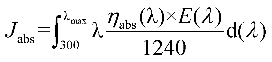 | (6) |
The charge separation efficiency (ηsep) and charge injection efficiency (ηinj) were tested with a hole scavenger, and the equation is as follows:42
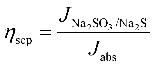 | (7) |
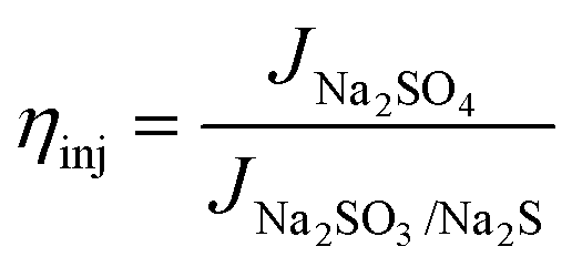 | (8) |
Computational methods
First-principles calculations were performed using density functional theory (DFT) within the Vienna ab initio simulation package (VASP), employing the projector-augmented wave (PAW) method.43,44 The exchange-functional was handled using the Perdew–Burke–Ernzerhof (PBE)45 functional. The DFT-D3 correction46 was adopted to describe weak interactions between atoms. The cut-off energy of the plane-wave basis was set at 450 eV in structural optimization. To optimize both the geometry and lattice size, Brillouin zone integration was conducted using 3 × 3 × 3 Monkhorst–Pack k-point sampling. The self-consistent calculations employed a convergence energy threshold of 10−5 eV. The equilibrium geometries and lattice constants were optimized with maximum stress on each atom within 0.02 eV Å−1. The isosurface level of charge density difference was set at 0.02 eV Å−3.Results and discussion
The octahedral oxygen-doped indium cadmium sulfide (OCIS) with 3D block structure was synthesized by a two-step process, including hydrothermal synthesis and subsequent annealing treatment (Fig. 1a). Uniform deposition can be observed in both the CIS (Fig. 1b and c) and OCIS (Fig. 1e and f). Similar octahedral morphology with a thickness and height of ∼0.8 μm (Fig. 1c and f) provides a structural basis for the deep diffusion doping. The high-resolution transmission electron microscopy (HRTEM) images of CIS and OCIS are illustrated in Fig. 1d and g. The synthesized CIS demonstrates a stripe spacing of 0.325 nm, which represents the typical (311) crystal plane (Fig. 1d). After oxygen doping, despite the similar lattice spacing, some broken lattice stripes can be detected (Fig. 1g), indicating that the oxygen has been successfully doped without structural collapse in the OCIS. Uniform distribution of the different elements, including Cd, In, S and O, was further verified through the energy-dispersive spectroscopy (EDS) elemental mapping in Fig. 1h. Furthermore, compared with the elemental composition of the CIS (Fig. S1†), OCIS demonstrates an increasing O content and a decreasing S content, indicating that the doping O atoms may replace the original S sites.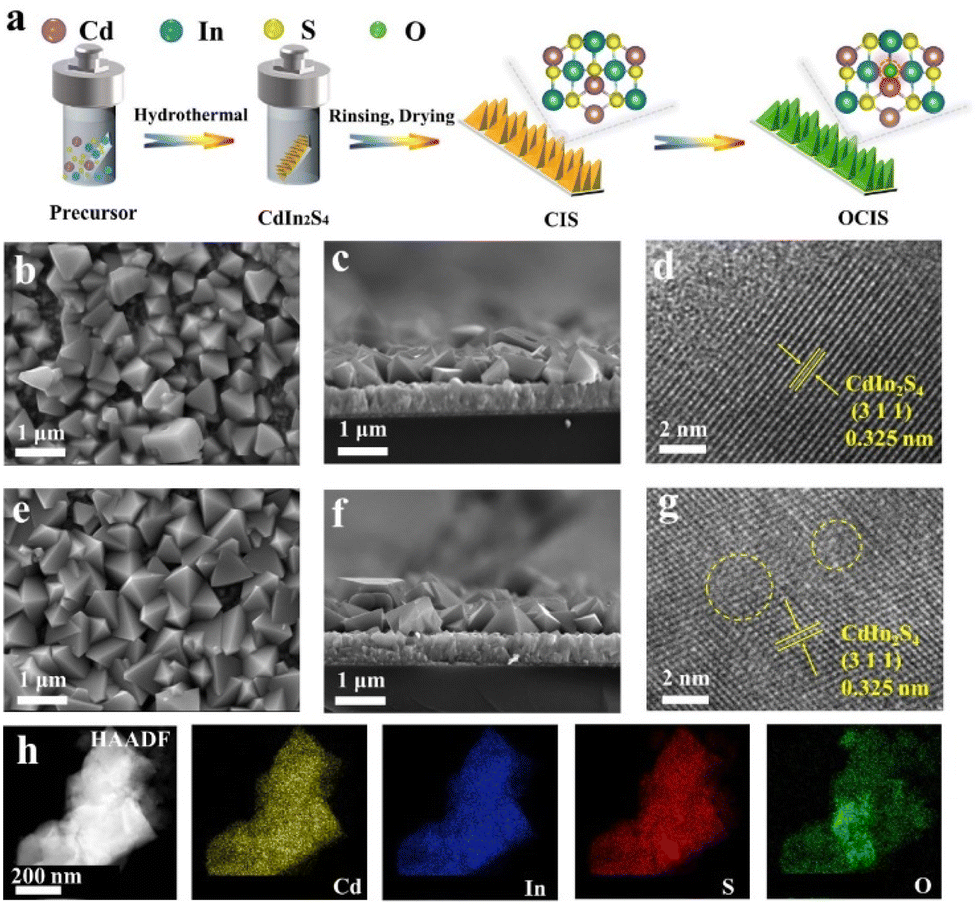 | ||
| Fig. 1 (a) The synthetic schematic for the OCIS photoanode. The top-view SEM images of (b) CIS, and (e) OCIS. The cross-sectional SEM images of (c) CIS and (f) OCIS. HRTEM images of (d) CIS and (g) OCIS. (h) EDS mapping of OCIS. | ||
XRD analysis was employed to investigate the crystalline phases of the OCIS photoanode (Fig. 2a).47 The diffraction peaks at about 14.14°, 23.18°, and 27.25° are ascribed to the (111), (220) and (311) planes, respectively.48 Negligible diffraction changes between OCIS and CIS further indicate the stability of the crystal form. Raman spectroscopy was applied to discern structural changes in OCIS. The peaks at 273, 308, 340 and 363 cm−1 correspond to the CIS (Fig. 2b).49 Remarkably, the peak at 363 cm−1, attributed to surface phonons of the anion,49 depicts a blue shift in OCIS. This phenomenon can be ascribed to the higher electronegativity of oxygen in OCIS. A similar influence was also detected in the FTIR analysis (Fig. S2†).
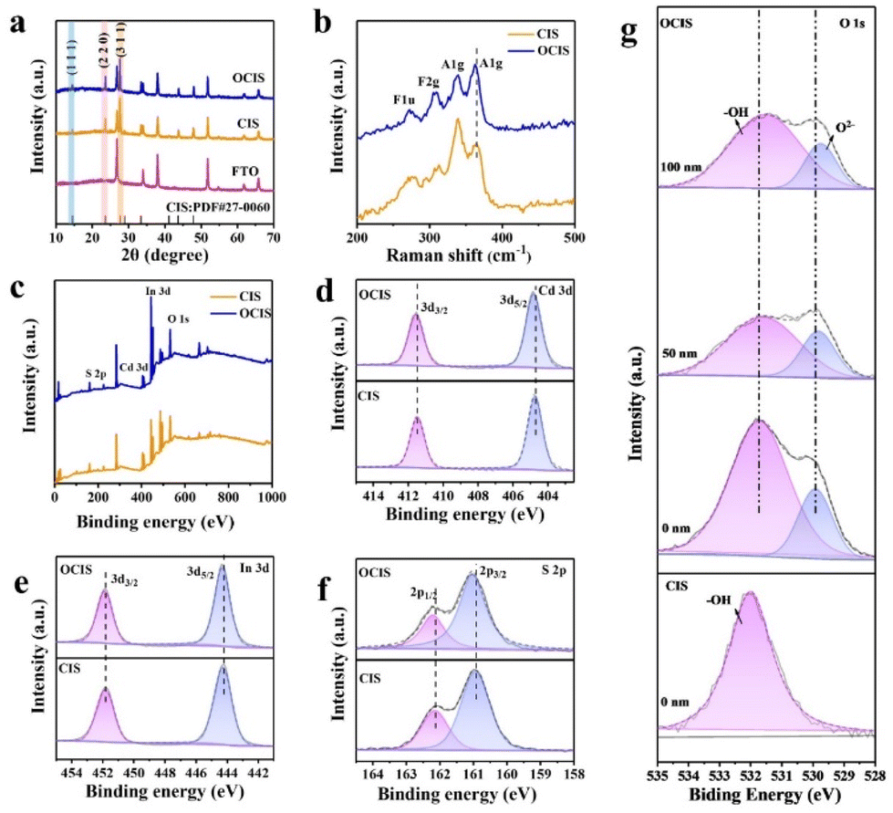 | ||
| Fig. 2 (a) XRD patterns and (b) Raman spectra for CIS and OCIS. (c) Survey and high-resolution XPS spectra for (d) Cd 3d, (e) In 3d, and (f) S 2p. (g) O 1s of CIS and depth profile spectra for OCIS. | ||
XPS analysis was conducted to investigate the chemical compositions and chemical states of the OCIS.41 Survey XPS spectra (Fig. 2c) revealed that both OCIS and CIS consist of Cd, In, S, and O, consistent with the elemental mapping images. The Cd 3d spectra (Fig. 2d) can be resolved into two peaks at 404.6 and 411.4 eV, representing Cd 3d3/2 and Cd 3d5/2 of Cd2+. The In 3d spectra (Fig. 2e) display two peaks centered at 444.2 and 451.9 eV, corresponding to the 3d3/2 and 3d5/2 of In3+. It is worth noting that the Cd and In peaks in OCIS exhibit a positive shift, suggesting alterations in the chemical environment surrounding the Cd and In atoms following oxygen doping. In addition, the S spectra (Fig. 2f) with peaks at160.9 and 162.1 eV correspond to the 2p3/2 and 2p1/2 of S2−. The S peak of OCIS is positively shifted, which can be ascribed to the generation of S vacancies. S vacancies create the basis for oxygen doping. The most intuitive evidence of oxygen doping is proved by the XPS characteristic spectrum of O 1s. The peaks at 529.8 and 532.0 eV represent lattice oxygen and hydroxyl-adsorbed oxygen in OCIS (Fig. 2g).50 However, no lattice oxygen is observed in the CIS, which demonstrates the oxygen doping in OCIS. Subsequently, the depth-dependent XPS profile was recorded for OCIS (Fig. 2g). The characteristic peak of lattice oxygen in OCS shows the lower signal intensity and a slight shift towards lower binding energy, with the increase of detection depth, demonstrating the diffusion of oxygen doping from the surface to the bulk phase in OCIS.
To assess the PEC water splitting performance, the OCIS and CIS photoanodes were exposed to simulated sunlight in 0.5 M Na2SO4 electrolyte. As shown in Fig. 3a and b, owing to the severe carrier recombination and sluggish migration of carriers, the CIS photoanode displays a low photocurrent density of 1.19 mA cm−2 at 1.23 V vs. RHE. After the oxygen doping, the OCIS photoanode achieved a photocurrent density of 3.69 mA cm−2 at 1.23 V vs. RHE, threefold higher than that of the CIS. Furthermore, cis-Ar (annealing CIS in Ar atmosphere at 300 °C for 2 h) demonstrates a similar photocurrent density of 1.31 mA cm−2 to that of CIS, but much lower than the value of OCIS, successfully excluding the influence of pyrolysis (Fig. S3†). Meanwhile, the onset potential (Von) of the OCIS is negatively shifted to 0.188 V vs. RHE. Even compared with the other reported metal sulfides, the catalytic performance is still exceptional (Table S1†). In addition, 208 μmol of hydrogen and 93 μmol of oxygen were collected after 2 h of the chronopotentiometry test (Fig. S4†). The calculated faradaic efficiencies (Fig. S5†) of O2 production are above 90%, representing that a great number of the photogenerated carriers participated in the O2 evolution, rather than self-oxidation. This revealing value helps to emphasize the importance of the gradient doping. After the addition of a hole sacrificial agent, the oxygen generation (Fig. S6†) was effectively suppressed. The catalytic stability of OCIS photoanode was evaluated by chronoamperometry test. As shown in Fig. S7,† OCIS exhibits a maintained photocurrent density of 77% after 3600 s, much higher than that of CIS (54%). Moreover, the structural stability of the OCIS was also identified by the XRD pattens (Fig. S8†) and SEM characterization (Fig. S9†) before and after the chronoamperometry test.
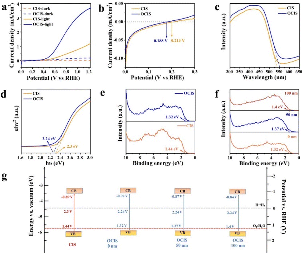 | ||
| Fig. 3 (a) LSV curves and (b) onset potentials for CIS and OCIS. (c) UV–vis absorption spectra and (d) corresponding Tauc plots for CIS and OCIS. (e) VB-XPS spectra for CIS and OCIS. (f) VB-XPS spectra for OCIS with different etching depths. (g) Energy level diagram for CIS and OCIS with gradient oxygen doping. | ||
The UV–vis absorption curves and Tauc plots for CIS and OCIS are shown in Fig. 3c and d. The light absorption of OCIS is higher than that of CIS because of the incorporation of additional electron energy levels. Valence band XPS (VB-XPS) was employed to determine the energy band structures of OCIS and CIS. As shown in Fig. 3e, the VB of the OCIS was calculated as 1.32 eV, closer to the potential of the oxidation reaction than that of the CIS (1.44 eV). Moreover, VBs of the OCIS with differing depths are also identified in Fig. 3f. Alongside the gradient oxygen doping, the VB of the OCIS gradually increased. Combining the information from the VB-XPS and Tauc plot, the bended energy band (Fig. 3g) was successfully constructed in OCIS from the surface to the bulk, thus confirming the construction of a microscale built-in electric field.7,51,52 The electric field effectively enhances the migration and separation of charge carriers.48,53,54
Although doping strategies can efficiently enhance the PEC performance by optimizing the band structure, dopants may also serve as centers for carrier recombination, therefore hindering the further enhancement of their PEC performance.55 Aiming to balance the bidirectional influence, CIS with differing lattice oxygen doping contents (from 18.33 to 53.91%) were rationally designed (Fig. S10–S15 and Table S2†). As the lattice oxygen content increased from 18.33 to 21.62%, the photocurrent density significantly improved from 1.38 to 3.62 mA cm−2 (Fig. S16, S17 and Table S2†). However, after further advancing the content from 21.62 to 53.91%, the photocurrent density decreased (Fig. S16, S17 and Table S2†). This variation trend is highly concordant with the reported bidirectional influence of the dopants. Accordingly, 21.62% (OCIS) seems to be the optimal oxygen doping content, reducing the recombination risk at the doping centers to the minimum.
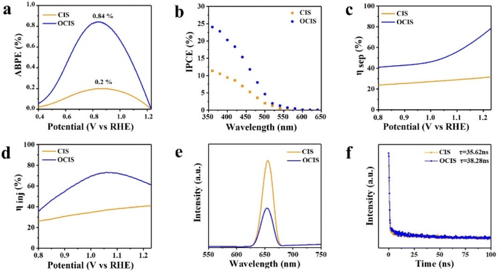
Based on the above-mentioned research, the following PEC tests were carried out with OCIS. The applied bias photon-to-current efficiency (ABPE) values of OCIS, as obtained from the J–V plots, show a peak value of 0.84% at 0.83 V vs. RHE, significantly surpassing the performance of reference CIS (0.2%, Fig. 4a). This result proves that under a certain bias voltage, the proportion of input solar energy converted into hydrogen energy increases significantly with the gradient oxygen doping-induced built-in electric field. Meanwhile, the incident monochromatic photon–electron conversion efficiency (IPCE) was also adopted to illustrate the photoresponse of the OCIS photoanode (Fig. 4b). Besides the extended adsorption range, the IPCE value of OCIS is significantly improved in the wavelength range of 350–500 nm. As a result of the reflection and refraction of incident light, it is important to further study the absorbing photon-to-current conversion efficiency (APCE) of the photoelectric anode.56 The APCE value of the OCIS photoanode (Fig. S18†) also increased in comparison with that of CIS, revealing that the photocurrent enhancement is also related to the improvement of the carrier separation efficiency.
 | ||
| Fig. 4 (a) ABPE and (b) IPCE for CIS and OCIS. (c) Charge separation efficiency and (d) charge injection efficiency of CIS and OCIS. (e) Steady-state PL spectra for CIS and OCIS with excitation wavelength λex = 325 nm. (f) TRPL decay spectra for CIS and OCIS. | ||
The ηabs of OCIS is shown in Fig. S19.† The enhanced ηabs of OCIS can be ascribed to the narrowed bandgap after gradient O doping, hence leading to increased light absorption and utilization. The ηsep and ηinj were estimated by using a mixture of 0.25 M Na2S and 0.35 M Na2SO3 as a hole sacrificing reagent. The corresponding photocurrent curves are displayed in Fig. S21.† The calculated ηsep is shown in Fig. 4c. As determined, with the microscale built-in electric field, the ηsep of OCIS is greatly improved after the gradient oxygen doping. Moreover, OCIS also displays a higher value of ηinj., indicating efficient recombination reduction. To further explore the migration and separation behaviour of photogenerated carriers in OCIS, PL spectroscopy was conducted.57 As predicted, the emission intensity of OCIS was significantly quenched (Fig. 4e). Stronger transient photocurrent response of OCIS also validates the promoted carrier migration (Fig. S20†). The carrier life of the photoanode was determined through TRPL spectroscopy.58 A double exponential decay function was used to analyze the TRPL decay lifetime measurements. The shorter lifetime component reflects the capture of photoexcited charge carriers associated with defects and interband transition recombination. The longer lifetime components describe the dynamics of surface-associated charge carriers.34 Compared with the original CIS, the carrier life of OCIS increased from 35.62 to 38.28 ns (Fig. 4f), demonstrating that the gradient oxygen doping-induced built-in electric field promotes bulky separation. The detailed fitting data is provided in Table S3.†
EIS also provides insights into the kinetics of the OER process (Fig. 5a and Table S3†). The illustration of Fig. 5a represents the equivalent circuit of the plot. The series resistance (Rs) signifies the impedance between the photoanode and FTO, while the charge-transfer impedance (Rct) represents the impedance between the electrolyte and the photoanode.59 Amazingly, OCIS exhibits a smaller semicircle diameter, which indicates that the gradient oxygen doping-induced built-in electric field is beneficial for carrier migration from the photoanode/electrolyte interface to the internal part. Furthermore, the active specific surface areas of OCIS and CIS were determined through CV, as shown in Fig. S22.† The calculated double-layer capacitance (Cdls) was obtained from CV.60 The steeper the slope, the more active sites on the photoanode surface. Compared with the CIS photoanode, the OCIS photoanode exhibits more active sites (Fig. 5b). This effect can be attributed to gradient oxygen doping, promoting the exposure of additional catalytic active areas.
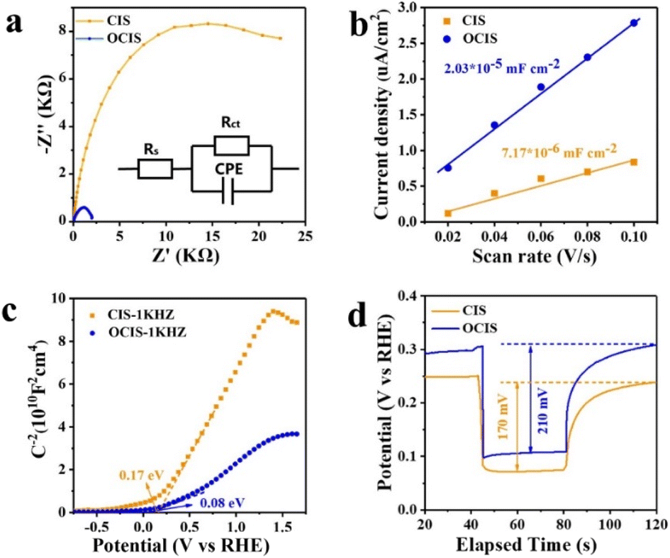 | ||
| Fig. 5 (a) The EIS Nyquist plots for CIS and OCIS under illumination. (b) Current densities of Cdls of CIS and OCIS. (c) M–S plots for CIS and OCIS in dark. (d) OCP measurements under dark and light conditions for CIS and OCIS. | ||
To further elucidate the effect of gradient oxygen doping, the M–S was measured in the dark at 10 kHz.61 The flat band potential and carrier density are calculated by the equation:62
| 1/C2 = (2/qεεε0NdA2)[(V − VFB) − kBT/q] | (9) |
| Eredox − Von = Vph − ηk | (10) |
Moreover, the regulation of the electronic structure of CIS by oxygen doping was studied by density functional theory (DFT) calculations. The structural model of pristine CIS is presented in Fig. 6a. The structural model of oxygen-doped OCIS is derived from pristine CIS with three sulfur atoms substituted with oxygen atoms (Fig. 6b). The content of lattice oxygen is similar to the XPS characterization result (4.32%). The calculated bandgap of OCIS (0.93 eV, Fig. 6d) is remarkably smaller than that of CIS (1.2 eV, Fig. 6c), suggesting that the oxygen heteroatoms can narrow the bandgap. This trend aligns with the experimental findings presented in Fig. 3d. Furthermore, the density of states (DOS) diagram of CIS (Fig. 6e) reveals that the Cd 4d orbitals and S 3P orbitals form the VB, and the CB primarily consists of S 3p orbitals. As oxygen atoms replace sulfur atoms in the unit cell of OCIS, the VB exhibits a slight upward shift towards the Fermi level, while the CB exhibits a drastic downward shift (Fig. 6f), which agrees well with the reduced bandgap.3 Notably, the discrepancy between the calculated and experimentally determined bandgaps can be ascribed to the recognized limitations of DFT calculations.64,65
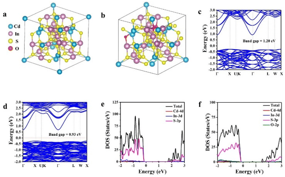 | ||
| Fig. 6 Side view of (a) bulk CdIn2S4 and (b) bulk CdIn2S4 with three S atoms replaced by O atoms. Band structure of (c) CIS and (d) OCIS. Density of states of (e) CIS and (f) OCIS. | ||
Conclusions
In summary, we constructed an OCIS photoanode with a microscale built-in electric field using a combined hydrothermal and annealing process. Oxygen doping can lead to an upward shift of the VB in CIS, as well as a reduction in the bandgap. Hence, band bending can be generated from the surface to the bulk phase by means of the gradient oxygen doping. The constructed built-in electric field can reach a depth of about ∼100 nm, thus accelerating the migration and separation of charge carriers over a wide range. Additionally, gradient oxygen doping increases the active area on the surface. By varying the synthetic conditions, the optimal OCIS not only minimizes the negative effect of dopants as electron–hole recombination centers, but also maximizes the positive effect of oxygen doping. This work provides an approach for enhancing the photoanode by constructing a microscale built-in electric field from the view point of bulky architecture, thereby improving its PEC performance.Author contributions
Jingwen Sun: conceptualization, resources, writing – review & editing. Shangling Han: conceptualization, methodology, investigation, writing – original draft. Fanglei Yao: data curation, validation. Ruixin Li: data curation. Chenchen Fang: data curation. Xiaoyuan Zhang: data curation. Yaya Wang: validation. Xuefeng Xu: validation. Di Wu: validation. Kai Liu: validation. Pan Xiong: supervision. Junwu Zhu: supervision, resources, project administration.Conflicts of interest
There are no conflicts to declare.Acknowledgements
This work was supported by the Natural Science Foundation of China (52372201) and the Fundamental Research Funds for the Central Universities (No. 30922010707). The authors would like to thank Hefei advanced computing center for performing the numerical computations. We appreciate eceshi (https://www.eceshi.com) for the XPS analysis.References
- X. Liu, J. Iocozzia, Y. Wang, X. Cui, Y. Chen, S. Zhao, Z. Li and Z. Lin, Energy Environ. Sci., 2017, 10, 402 RSC.
- M. Kim, B. Lee, H. Ju, J. Y. Kim, J. Kim and S. W. Lee, Adv. Mater., 2019, 31, 1903316 CrossRef PubMed.
- Y. Kuang, Q. Jia, G. Ma, T. Hisatomi, T. Minegishi, H. Nishiyama, M. Nakabayashi, N. Shibata, T. Yamada, A. Kudo and K. Domen, Nat. Energy, 2016, 2, 16191 CrossRef.
- Q. Wang and K. Domen, Chem. Rev., 2020, 120, 919 CrossRef CAS PubMed.
- C. Xu, W. Sun, Y. Dong, C. Dong, Q. Hu, B. Ma and Y. Ding, J. Mater. Chem. A, 2020, 8, 4062–4072 RSC.
- T. Yao, X. An, H. Han, J. Q. Chen and C. Li, Adv. Energy Mater., 2018, 8, 1800210 CrossRef.
- W. Tian, C. Chen, L. X. Meng, W. W. Xu, F. R. Cao and L. Li, Adv. Energy Mater., 2020, 10, 1903951 CrossRef CAS.
- J. Yadav and J. P. Singh, J. Alloys Compd., 2022, 925, 166684 CrossRef CAS.
- X. Li, S. Liu, K. Fan, Z. Liu, B. Song and J. Yu, Adv. Energy Mater., 2018, 8, 1800101 CrossRef.
- H. Li, C. Chen, X. Huang, Y. Leng, M. Hou, X. Xiao, J. Bao, J. You, W. Zhang and Y. Wang, J. Power Sources, 2014, 247, 915 CrossRef CAS.
- K. E. Dekrafft, C. Wang and W. Lin, Adv. Mater., 2012, 24, 2014 CrossRef CAS PubMed.
- P. Zhang, L. Yu and X. W. Lou, Angew. Chem., Int. Ed., 2018, 57, 15076 CrossRef CAS PubMed.
- P. Li, X. Chen, H. He, X. Zhou, Y. Zhou and Z. Zou, Adv. Mater., 2018, 30, 1703119 CrossRef PubMed.
- A. Y. Zhang, W. Y. Wang, J. J. Chen, C. Liu, Q. X. Li, X. Zhang, W. W. Li, Y. Si and H. Q. Yu, Energy Environ. Sci., 2018, 11, 1444 RSC.
- S. Shen, S. A. Lindley, X. Chen and J. Z. Zhang, Energy Environ. Sci., 2016, 9, 2744–2775 RSC.
- L. Meng, D. Rao, W. Tian, F. Cao, X. Yan and L. Li, Angew. Chem., Int. Ed., 2018, 57, 16882–16887 CrossRef CAS PubMed.
- D. Wang, T. Sheng, J. Chen, H. F. Wang and P. Hu, Nat. Catal., 2018, 1, 291 CrossRef CAS.
- W. Zhang, H. He, H. Li, L. Duan, L. Zu, Y. Zhai, W. Li, L. Wang, H. Fu and D. Zhao, Adv. Energy Mater., 2021, 11, 2003303 CrossRef CAS.
- G. Radovsky, R. Popovitz-Biro, M. Staiger, K. Gartsman, C. Thomsen, T. Lorenz, G. Seifert and R. Tenne, Angew. Chem., Int. Ed., 2011, 50, 12316 CrossRef CAS PubMed.
- M. M. Meshesha, K. Kannan, D. Chanda, J. Gautam, S. G. Ang and B. L. Yang, Mater. Today Chem., 2022, 26, 101216 CrossRef CAS.
- A. R. Fareza, F. A. A. Nugroho and V. Fauzia, ACS Appl. Nano Mater., 2022, 5, 16051 CrossRef CAS.
- J. Gao, J. Hu, Y. Wang, L. Zheng, G. He, J. Deng, M. Liu, Y. Li, Y. Liu and H. J. Zhou, J. Solid State Chem., 2022, 307, 122737 CrossRef CAS.
- Y. M. Lin, W. Q. Fang, R. Z. Xv and L. J. Fu, Hydrogen Energy, 2022, 47, 33361–33373 CrossRef CAS.
- Y. Q. Chen, Y. F. Cheng, J. F. Zhao, W. W. Zhang, J. H. Gao, H. Miao and X. Y. Hu, J. Colloid Interface Sci., 2022, 627, 1047–1060 CrossRef CAS PubMed.
- C. Y. Toe, S. Zhou, M. Gunawan, X. Lu, Y. H. Ng and R. Amal, J. Mater. Chem. A, 2021, 36, 20277–20319 RSC.
- Y. Choi, M. Beak and K. Yong, Nanoscale Adv., 2014, 6, 8914–8918 RSC.
- H. Kaga, Y. Tsutsui, A. Nagane, A. Iwase and A. Kudo, J. Mater. Chem. A, 2015, 3, 21815–21823 RSC.
- J. H. Huang, Q. C. Shang, Y. Y. Huang, F. M. Tang, Q. Zhang, Q. H. Liu, S. Jiang, F. C. Hu, W. Liu, Y. Luo, T. Yao, Y. Jiang, Z. Y. Pan, Z. H. Sun and S. Q. Wei, Angew. Chem., Int. Ed., 2016, 55, 2137–2141 CrossRef CAS PubMed.
- M. Zhou, Z. Liu, Q. Song, X. Li, B. Chen and Z. Liu, Appl. Catal., B, 2019, 244, 188–196 CrossRef CAS.
- J. P. Song, P. F. Yin, J. Mao, S. Z. Qiao and X. W. Du, Nanoscale, 2017, 9, 6296–6301 RSC.
- L. Mu, Y. Zhao, A. Li, S. Wang, Z. Wang, J. Yang, Y. Wang, T. Liu, R. Chen, J. Zhu, F. Fan, R. Li and C. Li, Energy Environ. Sci., 2016, 9, 2463–2469 RSC.
- S. Bai, X. Li, Q. Kong, R. Long, C. Wang, J. Jiang and Y. Xiong, Adv. Mater., 2015, 27, 3444–3452 CrossRef CAS PubMed.
- L. Meng, M. Wang, H. Sun, W. Tian, C. Xiao, S. Wu, F. Cao and L. Li, Adv. Mater., 2020, 32, 2002893 CrossRef CAS PubMed.
- S. Li, L. Meng, W. Tian and L. Li, Adv. Energy Mater., 2022, 12, 2200629 CrossRef CAS.
- T. Wang, Z. Luo, C. Li and J. Gong, Chem. Soc. Rev., 2014, 43, 7469 RSC.
- Y. H. Hou, T. Z. Li, S. C. Yan and Z. G. Zou, Appl. Catal., B, 2020, 269, 118777 CrossRef CAS.
- Y. Yu, Y. Huang, Y. Yu, Y. Shi and B. Zhang, Nano Energy, 2018, 43, 236 CrossRef CAS.
- C. Y. Yang, Z. Wang, T. Q. Lin, H. Yin, X. J. Lu, D. Y. Wan, T. Xu, C. Zheng, J. H. Lin, F. Q. Huang, X. M. Xie and M. H. Jiang, J. Am. Chem. Soc., 2013, 135, 17831–17838 CrossRef CAS PubMed.
- W. Yang, L. Zhang, J. Xie, X. Zhang, Q. Liu, T. Yao, S. Wei, Q. Zhang and Y. Xie, Angew. Chem., Int. Ed., 2016, 55, 6716 CrossRef CAS PubMed.
- Z. Chen, T. F. Jaramillo, T. G. Deutsch, A. Kleiman-Shwarsctein, A. J. Forman, N. Gaillard, R. Garland, K. Takanabe, C. Heske, M. Sunkara and E. W. McFarland, J. Mater. Res., 2010, 25, 3–16 CrossRef CAS.
- L. Meng, M. Wang, H. Sun, W. Tian, C. Xiao, S. Wu, F. Cao and L. Li, Adv. Mater., 2020, 32, 2002893 CrossRef CAS PubMed.
- D. K. Zhong, S. Choi and D. R. Gamelin, J. Am. Chem. Soc., 2011, 133, 18370–18377 CrossRef CAS PubMed.
- J. Hafner, J. Comput. Chem., 2008, 29, 2044–2078 CrossRef CAS PubMed.
- P. E. Blöchl, Phys. Rev. B, 1994, 50, 17953 CrossRef PubMed.
- J. P. Perdew, K. Burke and M. Ernzerhof, Phys. Rev. Lett., 1996, 77, 3865 CrossRef CAS PubMed.
- S. Grimme, J. Comput. Chem., 2006, 27, 1787 CrossRef CAS PubMed.
- J. Zheng, Y. Lyu, R. Wang, C. Xie, H. Zhou, S. P. Jiang and S. Wang, Nat. Commun., 2018, 9, 3572 CrossRef PubMed.
- B. B. Kale, J. O. Baeg, S. M. Lee, H. Chang, S. J. Moon and C. W. Lee, Adv. Funct. Mater., 2006, 16, 1349 CrossRef CAS.
- W. Unger, B. Farnworth, J. Irwin and H. Pink, Solid State Commun., 1978, 25, 913–915 CrossRef CAS.
- J. Hou, S. Cao, Y. Sun, Y. Wu, F. Liang, Z. Lin and L. Sun, Adv. Energy Mater., 2018, 8, 1701114 CrossRef.
- H. Huang, B. Dai, W. Wang, C. Lu, J. Kou, Y. Ni, L. Wang and Z. Xu, Nano Lett., 2017, 17, 3803 CrossRef CAS PubMed.
- C. Zeng, Q. Zeng, C. Dai and Y. Hu, Dalton Trans., 2020, 49, 9213 RSC.
- S. Wang, B. Y. Guan, Y. Lu, X. W. Lou and J. Am, Chem. Soc., 2017, 139, 17305 CrossRef CAS PubMed.
- L. Huang, B. Li, B. Su, Z. Xiong, C. Zhang, Y. Hou, Z. Ding and S. Wang, J. Mater. Chem. A, 2020, 8, 7177 RSC.
- C. Yang, Z. Wang, T. Lin, H. Yin, X. Lü, D. Wan, T. Xu, C. Zheng, J. Lin, F. Huang, X. Xie and M. Jiang, J. Am. Chem. Soc., 2013, 135, 17831–17838 CrossRef CAS PubMed.
- H. M. Wang, Y. G. Xia, H. P. Li, X. Wang, Y. Yu, X. L. Jiao and D. R. Chen, Nat. Commun., 2020, 11, 3078 CrossRef CAS PubMed.
- W. Xu, W. Gao, L. Meng, W. Tian and L. Li, Adv. Energy Mater., 2021, 11, 2101181 CrossRef CAS.
- X. Song, G. Wei, J. Sun, C. Peng, J. Yin, X. Zhang, Y. Jiang and H. Fei, Nat. Catal., 2020, 3, 1027 CrossRef CAS.
- W. Xu, L. Meng, W. Tian, S. Li, F. Cao and L. Li, Small, 2022, 18, 2105240 CrossRef CAS PubMed.
- S. Hao, L. Chen, C. Yu, B. Yang, Z. Li, Y. Hou, L. Lei and X. Zhang, ACS Energy Lett., 2019, 4, 952 CrossRef CAS.
- N. Hirayama, H. Nakata, H. Wakayama, S. Nishioka, T. Kanazawa, R. Kamata, Y. Ebato, K. Kato, H. Kumagai, A. Yamakata, K. Oka and K. Maeda, J. Am. Chem. Soc., 2019, 141, 17158 CrossRef CAS PubMed.
- J. H. Kim, J. W. Jang, Y. H. Jo, F. F. Abdi, Y. H. Lee, R. Van de Krol and J. S. Lee, Nat. Commun., 2016, 7, 13380 CrossRef CAS PubMed.
- C. Du, X. Yang, M. T. Mayer, H. Hoyt, J. Xie, G. McMahon, G. Bischoping and D. Wang, Angew. Chem., Int. Ed., 2013, 52, 12692 CrossRef CAS PubMed.
- Q. Li, H. Meng, P. Zhou, Y. Zheng, J. Wang, J. Yu and J. Gong, ACS Catal., 2013, 3, 882–889 CrossRef CAS.
- C. Steiner, J. Gebhardt, M. Ammon, Z. C. Yang, A. Heidenreich, N. Hammer, A. Görling, M. Kivala and S. Maier, Nat. Commun., 2017, 8, 14765 CrossRef CAS PubMed.
Footnotes |
| † Electronic supplementary information (ESI) available. See DOI: https://doi.org/10.1039/d3nr05609k |
| ‡ These authors contributed equally to this work. |
| This journal is © The Royal Society of Chemistry 2024 |