
Energy-efficient resistive switching synaptic devices based on patterned Ag nanotriangles with tunable gaps fabricated using plasma-assisted nanosphere lithography†
Shubham K. Mehta ,
Indrajit Mondal,
Bhupesh Yadav and
Giridhar U. Kulkarni*
,
Indrajit Mondal,
Bhupesh Yadav and
Giridhar U. Kulkarni*
Chemistry & Physics of Materials Unit, Jawaharlal Nehru Centre for Advanced Scientific Research, Jakkur P. O., Bangalore-560064, India. E-mail: kulkarni@jncasr.ac.in
First published on 9th September 2024
Abstract
The development of synaptic devices featuring metallic nanostructures with brain-analog hierarchical architecture, capable of mimicking cognitive functionalities, has emerged as a focal point in neuromorphic computing. However, existing challenges, such as inconsistent and unpredictable switching, high voltage requirements, unguided filament formation, and detailed fabrication processes, have impeded technological progress in the domain. The present study addresses some of these challenges by leveraging periodic nanostructures of Ag fabricated via plasma-assisted nanosphere lithography (NSL). The triangular nanostructures with a preferred orientation offer enhanced localized electric fields, facilitating low voltage electromigration at the sharp edges to guide predictive filament formation. A thorough investigation into gap control between the nanostructures through oxygen plasma treatment enables the attainment of an optimized low switching voltage of 0.86 V and retention at an ultra-low current compliance of 100 nA. The optimized device consumes low power, typically in the fJ range, akin to biological neurons. Furthermore, the device showcases intriguing synaptic characteristics, including controlled transition from short- to long-term potentiation, associative learning, etc., projecting its potential in perceptive learning, memory formation, and brain-inspired computing. COMSOL Multiphysics simulation, supported by ex situ electron microscopic imaging, confirms the controlled and predictable filament formation facilitated by electric field enhancement across the strategic nanostructures. Thus, the work highlights the potential of NSL-based cost-effective fabrication techniques for realizing efficient and biomimetic synaptic devices for neuromorphic computing applications.
Introduction
In recent years, there has been tremendous progress in fabricating microelectronic devices to emulate brain functionalities, including short-term plasticity (STP), long-term potentiation (LTP), associative learning, and other cognitive processes.1–6 Such behavioral functionalities are born out of the ability of the active synaptic junction via accumulation and firing of the action potential. In the domain of artificial devices, such functionality is derived from the conductance state (and such properties) achieved by the device based on the strength and the sequence of arrival of inputs, much the way a memristor functions.7–9 Such a unique property has been realized in many ways through resistive switching and spintronics devices.10–12Among diverse resistive switching synaptic devices, namely electrochemical metallization (ECM), valence change memory (VCM), phase change memory (PCM), etc,13–17 ECM stands out for its exceptional control over filament formation and ultra-low power consumption.18,19 ECM is an electric field-driven phenomenon related to the atomic connection between nanostructures, where the gap between the nanostructure or nanocluster is crucial for resistive switching.20,21 There are various reports on gap-dependent electromigration-based devices.22–24 For instance, electron beam lithography (EBL)-fabricated Au nanostructure with a 54 to 62 nm gap was reported by Sakai and coworkers for the ECM-based conduction to control tunnelling resistance across the nanogaps.25 Bose et al. have worked on controllable switching of a self-assembled nanoparticle network, leading to atomic connections between the interparticle gaps.26 In another instance, for effective localization of electrons at the tip, Pt nano-junctions of gaps less than 2 nm have been fabricated using nanoimprint lithography, but the gaps were found to suffer with the migration of atoms under applied voltage.27 These systems used high voltages (>2 V) for the electromigration of metallic atoms between nanogap and complex lithographic fabrication. Concurrently, previous studies from our group have explored nanoscale Ag agglomerates formed through the dewetting of an Ag film. In such devices, electromigration occurs within the gaps of these Ag agglomerates at low voltages, enabling basic synaptic functions like STP, LTP, and associative learning with lower energy requirements. Furthermore, ECM-based devices demonstrate excellent device-to-device consistency, making them highly suitable for integration into crossbar array architectures.28,29 These self-formed structures offer stochastic filamentary-based cognitive functionalities.30–34
Achieving nanoscale structure with tunable nanogaps is crucial for ECM-based devices. However, fabricating such structures for synaptic devices typically demands laborious techniques like photolithography, EBL, etc.,35 which are intricate, costly, and time-intensive.36 In contrast, nanosphere lithography (NSL) offers a simple, scalable and inexpensive alternative for generating large-area array of 2D nanostructures with precise control over shape, size, and interparticle spacing.37–39 This process relies on a disordered colloidal system that adopts the lowest available entropy to develop a self-assembled, ordered, and stable structure.38 Noble metal nanostructures produced via NSL have found applications in diverse fields, such as optical chemo-sensors and biosensors platforms.40–42 However, there are hardly any reports on its utilization for neuromorphic device fabrication.
In this work, we have fabricated two-terminal planar synaptic devices with Ag triangular nanostructures using NSL. Scanning electron microscopy (SEM) and transmission electron microscopy (TEM) have been employed to extract microscopic information pertaining to fabricated nanostructures. The metal bowtie gap was adjusted via an oxygen plasma treatment (OPT), allowing control over the nanosphere shadow to yield adjustable gaps between the nanostructures, thereby facilitating lowering of the threshold switching while also reducing power requirement per synapse. Furthermore, the device emulates controlled STP to LTP transition and association learning aided by an ECM-based filament formation, which is further corroborated via simulating the electric field distribution across nanostructures using COMSOL Multiphysics and an ex situ SEM. COMSOL simulation confirms that the electromigration of Ag follows the path between the bowtie tip where the electric field is localized. The study is the first of its kind using the scalable NSL method for neuromorphic device fabrication.
Experimental section
Device fabrication using nanosphere lithography
Initially, glass substrates of dimension 3.75 × 1.25 cm2 were ultrasonically cleaned successively in soap solution, deionized (DI) water, acetone, and isopropyl alcohol for 10 min each and then dried using N2 gas. A 10% polystyrene (PS) sphere solution (Bang Laboratory Inc.) with a 500 nm diameter was used for the NSL after dilution with ethanol at 1![[thin space (1/6-em)]](https://www.rsc.org/images/entities/char_2009.gif) :1 v/v%. At first, a Petri dish of diameter 5 cm was filled with water, and then the cleaned glass slide was placed inside at an angle of 45°. Next, a 10 μL pipette was used for adding the PS solution dropwise at the air–water interface. A bluish-green layer, confirming PS monolayer formation, appeared on the surface of the water after dropping 40 μL of the solution. Thereafter, another glass slide was used for transferring the monolayer on the glass slide. Subsequently, OPT (Henniker Plasma, HPT-100) was performed on the template to reduce the size of the PS sphere to the desired dimension. The OPT was performed for different durations from 60 to 300 s (30 s intervals) at a power of 100 W while keeping the oxygen flow rate at 20 sccm. Afterward, the monolayer was used as a shadow mask for Ag deposition. A thermal evaporator system (HHV ATS-500) was used to deposit 60 nm Ag. The deposition was carried out at a rate of 1.5 nm s−1 with the substrate holder rotation at 8 rev. per min to obtain a quasi-triangular (QT) structure. No rotation was used to form intact Ag triangles. Consequently, the PS monolayer was removed by using scotch tape. To complete the device fabrication, 100 nm thick Al electrodes of dimension 5 × 2 mm2 were deposited on the Ag nanostructure by using a shadow mask of 40 μm wide Cu wire.
:1 v/v%. At first, a Petri dish of diameter 5 cm was filled with water, and then the cleaned glass slide was placed inside at an angle of 45°. Next, a 10 μL pipette was used for adding the PS solution dropwise at the air–water interface. A bluish-green layer, confirming PS monolayer formation, appeared on the surface of the water after dropping 40 μL of the solution. Thereafter, another glass slide was used for transferring the monolayer on the glass slide. Subsequently, OPT (Henniker Plasma, HPT-100) was performed on the template to reduce the size of the PS sphere to the desired dimension. The OPT was performed for different durations from 60 to 300 s (30 s intervals) at a power of 100 W while keeping the oxygen flow rate at 20 sccm. Afterward, the monolayer was used as a shadow mask for Ag deposition. A thermal evaporator system (HHV ATS-500) was used to deposit 60 nm Ag. The deposition was carried out at a rate of 1.5 nm s−1 with the substrate holder rotation at 8 rev. per min to obtain a quasi-triangular (QT) structure. No rotation was used to form intact Ag triangles. Consequently, the PS monolayer was removed by using scotch tape. To complete the device fabrication, 100 nm thick Al electrodes of dimension 5 × 2 mm2 were deposited on the Ag nanostructure by using a shadow mask of 40 μm wide Cu wire.
Characterization and measurements
TEM (Thermo Fisher, TALOS F200S G2, 200 keV) was performed to observe the Ag nanostructure and its planer orientation. For imaging purpose, the Ag triangles from the glass were first lifted off using IPA drops and then transferred onto a TEM grid. Field emission scanning electron microscope (FESEM) images were taken using Apreo-2 SEM (Thermo Fisher Scientific Inc.). UV-Vis absorption spectra were collected using a spectrometer from Agilent (Cary Series). A source measure unit (SMU) (Keithley 2461) connected to two tungsten probes attached to an XYZ stage controller (Thorlabs Inc.) was used for all the electrical measurements, namely I–V sweeps, and pulsing. Dual I–V sweeps were taken with a proper time gap between the successive sweeps to avoid non-volatile switching of the device. ImageJ software was used to calculate the fill factor and nanogaps from the FESEM image analysis. COMSOL Multiphysics 6.1 was used to simulate the electric field distribution by using the AC/DC module. First, the geometry was fed using a binary image of the device and converted into a curve, and then the material corresponding to that was assigned. Then, the simulation was performed with extremely fine mesh.Results and discussion
Fabrication of the periodic nanostructure of Ag triangles involves fewer steps, as demonstrated schematically in Fig. 1a (see Experimental section for details). At first, PS nanoparticles of diameter ∼ 472.2 ± 10.2 nm (see the distribution profile in Fig. S1a†) were dispersed in 1:1 (v/v%) ethanol–water solution and then slowly spread onto the surface of water in a Petri dish. Nanoparticles self-assembled into a monolayer (see the FESEM image in Fig. 1b) due to the surface tension gradient (Marangoni effect) between water and the PS solution,43 causing the Marangoni force to move the suspended particles in an outward direction until covering the water surface completely. Next, the layer was dip-transferred onto a pre-cleaned glass substrate, as shown in the inset of Fig. 1b, portraying a uniform film with diffracted colors emanating from its periodic structure. Afterward, the monolayer, either as formed or after OPT, was used as a shadow mask for Ag deposition. Thereafter, the PS monolayer was removed to attain the Ag triangular nanostructure. The deposition was carried out in two ways – (i) with and (ii) without substrate holder rotation during thermal evaporation. While the former produced quasi-triangular (QT) nanostructures consisting of tiny discrete particles due to a glancing angle deposition (Fig. 1c), the latter resulted in intact triangular structures (see Fig. 1d) with varied gaps depending upon the OPT time (Tp).44 Without the OPT, triangles were largely spaced (as seen in Fig. 1d) with a gap ascribed to a larger shadow masking at the inter-nanosphere interfaces.45 The OPT leads to a reduction in the shadowing effect (Fig. 1e–h), for Tp = 90, 120, 150, and 240 s, respectively due to the PS size reduction45 (see Fig. S1b–e†), resulting in a decrement in nanogap between triangles, as depicted in the FESEM images in Fig. 1i–l. The PS spheres reduce their size (see Fig. S1f†) by reacting with the oxygen ions while liberating gases such as CO, CO2, etc.46 The rod-like nanobridge between the PS spheres has appeared with the OPT due to the melting and etching of the PS spheres with Tp.47 An increase in Tp shrinks the PS spheres and thins and breaks the nanobridge contact, leading to the non-closed-packed structure, as shown in Fig. 1e–h. Bright-contrast TEM images were captured to better visualize the Ag nanostructure and investigate the presence of any unwanted impurities (Fig. S2a–c†). The images along with the lattice parameters calculated from the selected area electron diffraction (SAED) pattern confirm the presence of metallic Ag (Fig. S2d and Table S1†) without impurities.
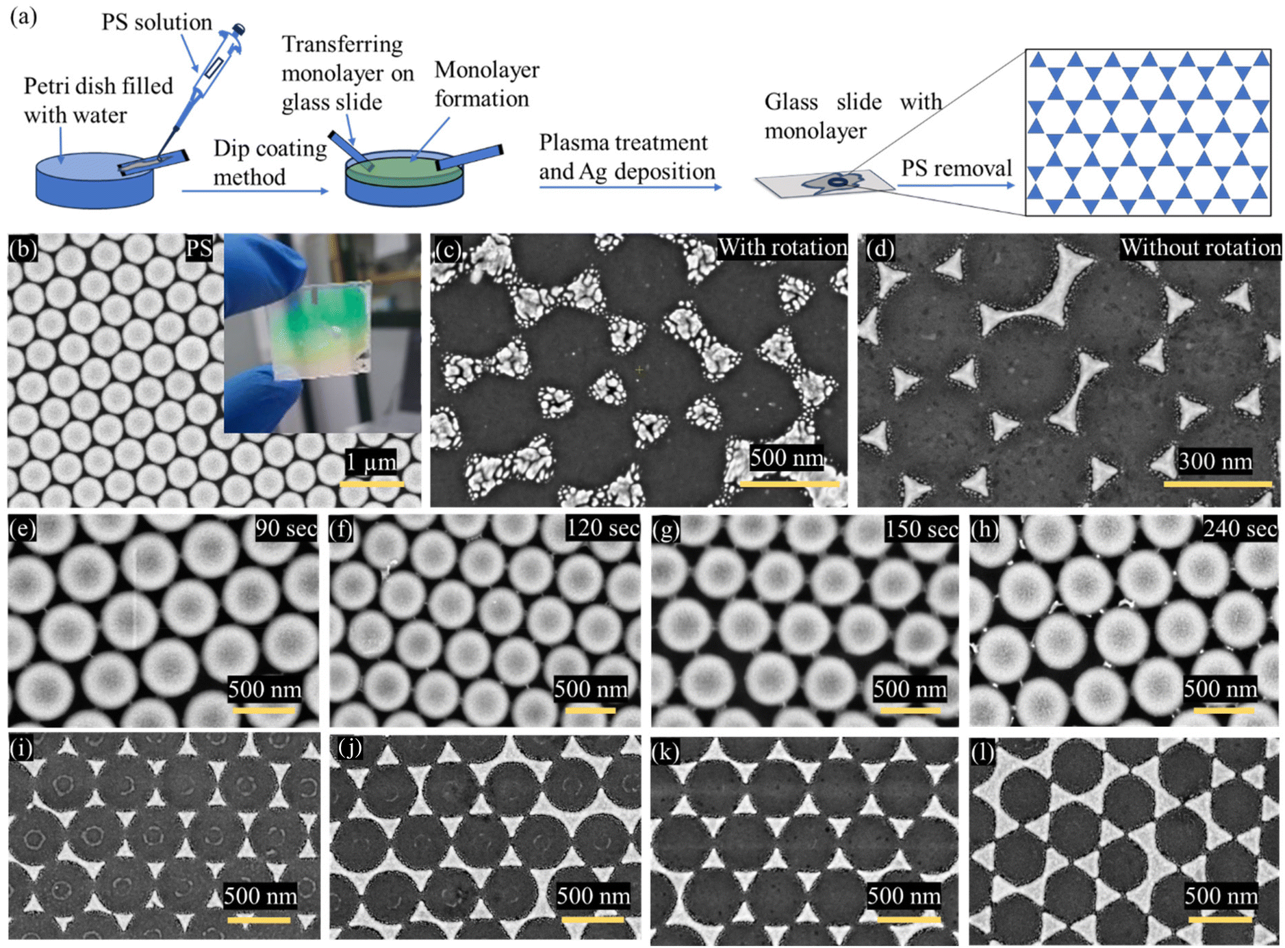 | ||
| Fig. 1 (a) Schematic illustrating the fabrication process of Ag triangular nanostructure by NSL. The process includes the Marangoni formation of a PS monolayer onto the water surface, followed by its transfer onto a glass substrate, partial plasma etching of PS, Ag deposition, and PS removal. FESEM images of (b) the PS monolayer template; inset showing the photograph of the template at a large scale. Ag nanostructures obtained (c) with and (d) without rotation of substrate holder during Ag deposition; (e), (f), (g), and (h) ordered structure of PS monolayers after OPT for 90, 120, 150, and 240 s, respectively; (i), (j), (k) and (l) respective Ag nanostructures after PS removal. | ||
To better understand the NSL in obtaining control over the structural parameter, the variation in Ag fill factor (shown as 1 − FF) and the corresponding average nanogap ‘d’ were plotted against TP values. ImageJ software was utilized to calculate the FF (as exemplified in Fig. 2a and Fig. S3a†) and ‘d’ (see Fig. S3b and Table S2†). The plot in Fig. 2b indicates that the OPT leads to a linear reduction in both ‘d’ and ‘1 − FF’ of Ag at rates of 0.4 nm s−1 and 0.06% s−1, respectively. As Tp increases, the size and shadowing effect of PS spheres decreases, and thus, the FF increases. UV-VIS absorbance spectroscopy was also performed to gain insight into the plasmonic effect of the periodic nanostructure. As depicted in Fig. 2c and d, the structure with d ∼ 78 nm shows a localized surface plasmon (LSPR) peak at 660 nm, which undergoes a red shift with the decreasing d. The red shift of the plasmonic peak originates from the coupling of plasma electrons between the Ag triangles.48 As the nanogap becomes smaller, the coupling between adjacent triangles increases, resulting in an easy exchange of electrons within the bowtie structure, thereby lowering the effective restoring force. As the force decreases, the resonant energy to induce the plasmonic coupling reduces, causing a red shift in the LSPR dipolar peak.49
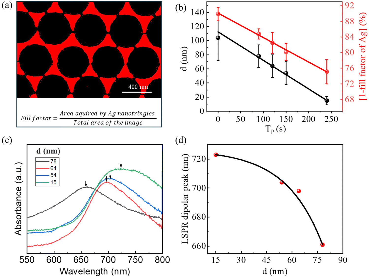 | ||
| Fig. 2 (a) Ag fill factor (FF) calculation from FESEM image. (b) Average nanogap ‘d’ and FF variation (shown as 1 − FF) with OPT time (TP), (c) absorption spectra of Ag superlattice structures prepared by following Tp of 90, 120, 150, and 240 s. (d) Variation of the corresponding LSPR dipolar peak with the nanogap. | ||
The unique bowtie structures were exclusively exploited in this study in fabricating neuromorphic devices, as schematically demonstrated in Fig. 3a, where the device analogy to the biological synapse is showcased. The release of neurotransmitters across the synapse between the pre and post-neurons helps in memory formation by adjusting synaptic weight in the biological systems.50 As depicted, the metallic triangular islands and the intermittent gaps in the device act as neurons and synapses, respectively. Also, the device conductance update serves as the synaptic weight in the device. The device containing a network of such synapse-like junctions resembles, in principle, the biological neural network structurally. The device fabrication was completed by forming Al electrodes spaced 40 μm apart on the periodic nanostructures (Fig. 3a). The unperturbed device exhibits an initial high resistance state (HRS) attributed to the presence of unconnected nanogaps between the electrodes. During an I–V sweep, the device transitions to low resistance state (LRS), with a high ON/OFF ratio (104), while device current being regulated by a specific current compliance (ICC) (Fig. 3b–e). Such transition could be attributed to the electric field aided electromigration of Ag across nanogaps.51 Due to the unipolar nature of the device, it has a nearly symmetric I–V sweep for positive and negative polarities, as shown in Fig. S4.† With the gradual withdrawal of voltage, the device automatically returns to the HRS state without requiring an opposite bias. When an opposite bias is applied, the device switches back to the LRS state. But LRS can be erased to the HRS by applying the voltage within a tiny window (∼200 mV) around the origin (red box in Fig. S4†). Further analysis related to the filament formation and its correlation to the structural geometry of Ag is detailed later.
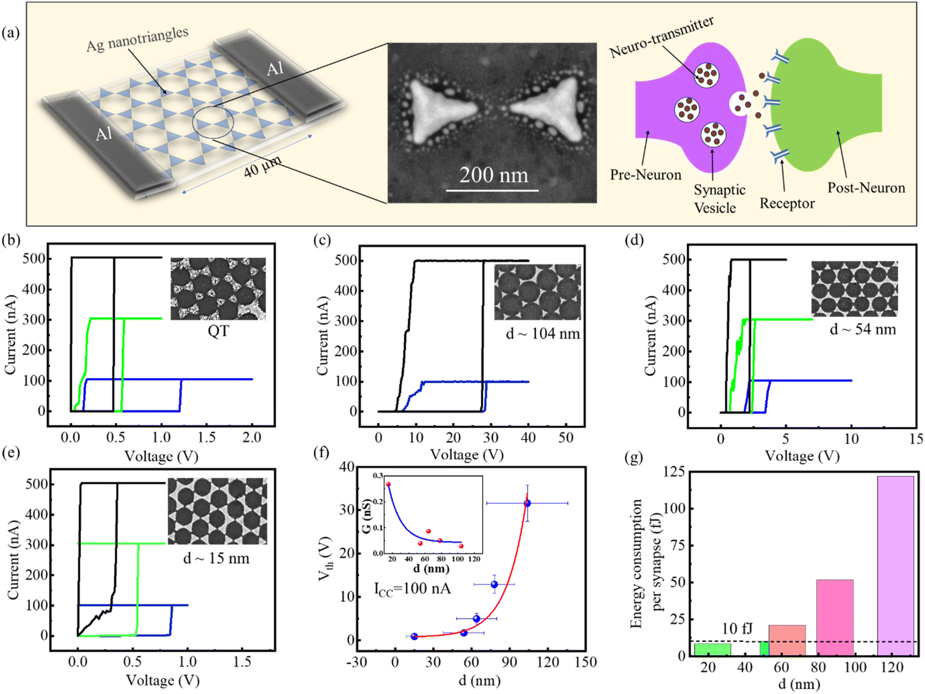 | ||
| Fig. 3 (a) Schematic of the device with a magnified bowtie structure resembling biological synapses. I–V characteristics of samples having (b) QT structure, (c) d ∼ 104 nm, (d) d ∼ 54 nm, and (e) d ∼ 15 nm, depicting a decreasing tendency of Vth with increasing ICC. (f) Vth variation with ‘d’. Inset shows the HRS conductance exponential decay with increase in nanogap at ICC = 100 nA. (g) Histogram comparing energy consumption per synapse between devices with different nanogaps. | ||
To begin with, the I–V sweeps were performed at a low ICC (100 nA) for each device (Fig. S5a†), resulting in higher forming voltages during HRS to LRS switching (see Fig. S5b† and histogram for the sequence of a sweep at each ICC in Fig. S5c†). The pristine devices initially require a high voltage to form a filamentary path. However, with repeated sweeps, the switching or threshold voltage decreased significantly (see Fig. S5e–i†). For a comprehensive analysis, I–V sweeps of several devices comprising QT and bowtie structures with different nanogaps are compared, as shown in Fig. 3b–e. Interestingly, the device with the lowest gap of 15 nm shows an ultra-low switching voltage (Vth) of only 300 mV at an ICC of 500 nA. The lowering of Vth could be attributed to the unique structural design of the nano-architecture, which helps in enhancing and concentrating the electric field during the sweep (later verified by COMSOL simulation). A similar Vth value was also obtained for the QT device. Nonetheless, the QT structure (Fig. S6a†) suffered from geometrical instability (see Fig. S6b†) upon repeated sweeping (Fig. S6c†), probably due to its scattered nature, leading to a drastic fluctuation in Vth, as shown in Fig. S6d.† Repeated voltage sweeps for all devices with different nanogaps are shown in Fig. S5d–i.† It is intriguing that Vth shows a decreasing trend with increasing ICC, which may be due to a better filament consolidation assisted by enhanced Joule heating at higher ICC.31 Device-to-device performance was examined using four devices (d ∼ 15 nm) named D1, D2, D3, and D4, as shown in the insets of Fig. S7b–e.† Initially, I–V sweeps were performed at an ICC of 100 nA, revealing higher forming voltages (Fig. S7a†). The switching voltage of devices drops with successive sweeps (1, 2, and 3) at each ICC value, 100, 300, and 500 nA (shown in Fig. S7b–e†). Apart from higher forming voltage, the devices exhibited lesser spread in threshold voltages, as depicted in Fig. S7f.† Furthermore, as seen in Fig. 3f, an exponentially increasing correlation is observed between the average Vth and ‘d’. Also, the Vth varies exponentially with nanogap number density (n/A), which was calculated using ImageJ software (see Fig. S8†). For a deeper analysis, the conductance of these devices in the HRS states was calculated from the slope of the I–V sweep till the threshold switching (see the inset in Fig. 3f). The result indicates an exponential decrement in the HRS conductance with d, inferring the device is in a tunneling regime; otherwise, a linear behavior is expected.52 The direct tunneling current ‘I’ decreases exponentially with the gap ‘d’, as given by the following equation,52
| I = A × V × exp(−B × d) | (1) |
| V = a × exp(B × d) | (2) |
Thus, Vth increases exponentially with the gap in the low ICC range (∼100 nA), where the conduction transpires majorly through tunneling. The stability study demonstrates that the device exhibits consistent threshold-switching behavior even after one year of storage under ambient conditions (see Fig. S9†).
A detailed analysis was performed to obtain per-synapse energy requirement, as shown in Fig. 3g, indicating an exponential increment in the energy consumption with the nanogap (see Fig. S10b†). The calculation (as shown in Note S1†) considers two probable synaptic connections (indicated by arrows 2 and 3 in Fig. S10a†) for each triangle. Remarkably, the device with d ∼ 15 nm consumes only 8.4 fJ per synapse, close to the limit of a biological synapse (10 fJ) and outperforming many literature reports.31
To emulate brain functionality such as weightage-dependent STP to LTP transition, appropriate voltage pulses were applied to devices after obtaining Vth from the I–V sweeps. The weightage was varied by using ICC of different amplitudes. Pulses with amplitudes of 2, 3, and 6 V (with 10 pulses of pulse width, tw = 50 ms and pulse interval, ti = 50 ms) were applied to devices with a QT structure, d ∼ 68 and 54 nm, respectively (Fig. 4a–c, respectively). The conductance retention behavior of the device after pulsing was monitored with a reading voltage (VR) of 10 mV. Intriguingly, with the increasing ICC, the retention time increased with nominal stochasticity (as shown in Fig. 4d), indicating a system apt for probabilistic computing with a high error tolerance.53 Furthermore, the rates of retention increment for d ∼ 54 (green) and d ∼ 64 nm (red) infer that STP to LTP transition is more favorable for lower gap devices. The same has also culminated from repeated pulsing measurements at different ICC (Fig. S11–S13†). Applying high electrical stress to a device can result in either the formation of fewer filaments with larger diameters or multiple weaker filaments. In the first scenario, further increasing the current compliance (ICC) enhances retention, leading to LTP. In the second scenario, however, the increased Joule heating from the high current causes the dissolution of the weaker filaments due to their limited current-carrying capacity, producing STP behavior.31 Notably, the device with the lowest d requires a minimum voltage of 0.8 V (conductance read by low voltage VR = 500 μV) and only 5 pulses with tw = 50 and ti = 50 ms sufficient to train the device. The device shows an STP to LTP transition with increased ICC (Fig. 4e), and a further enhanced memory formation with iterated training at each ICC (Fig. S14†). It is worth noting that a device with d ∼ 15 nm requires a much lower ICC for retention compared to other devices, depicting minimal energy consumption. Fig. 4f shows that the retention time exponentially increases with increase in ICC, which could be cognitively correlated with attentive learning.54 The overall ICC dependency may be understood from strengthening Ag filaments with the increasing ICC leading to higher retention.
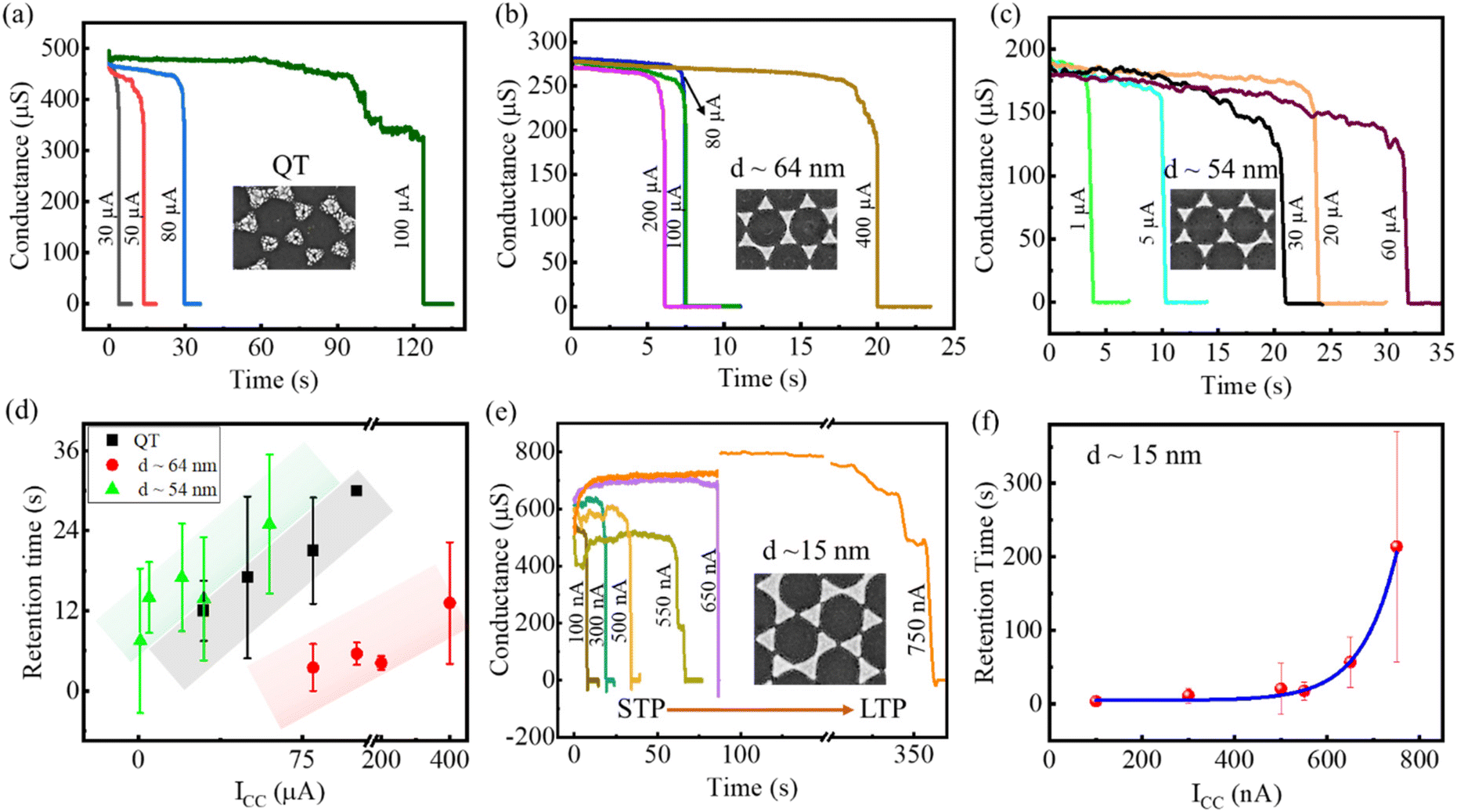 | ||
| Fig. 4 Memory retention and STP to LTP transition as a function of ICC for devices having (a) QT structure, (b) d ∼ 64 nm (c) d ∼ 54 nm. Retention time variation as a function of ICC for (d) QT structure, d ∼ 64 nm, and d ∼ 54 nm. (e) STP to LTP transition of conductance at low ICC (nA) of d ∼ 15 nm device and its (f) retention time versus ICC plot. | ||
The cognitive learning aspect of the device was demonstrated by emulating Pavlov's classical conditioning or associative learning, as shown in Fig. 5. In associative learning, the brain exhibits a response to a conditioned stimulus (such as a bell) after training involving repetitive association with an unconditioned stimulus (such as food). To emulate such behavior, the device was exposed to two different sets of pulses having an amplitude of 1.2 V (food) and 0.5 V (bell). Initially, a response was observed for the food; however, no response was observed for the bell pulse, as expected. During the training, food and bell pulse were applied concurrently to establish an association between the two signals. The device starts responding to bell pulse after the training. Creating an association between two unlinked stimuli shows the potential of the device to emulate numerous cognitive behaviors of the brain.
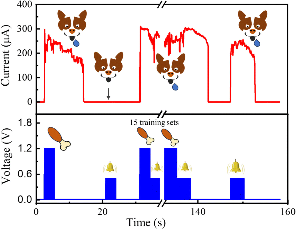 | ||
| Fig. 5 Emulation of classical conditioning using the device subjected to an appropriate training set of food (1.2 V) and bell (0.5 V) pulses. Before training, the response was observed only with the food pulse, whereas it was absent for the bell pulse. After training with 15 consecutive sets of food and bell pulses, the device responded to the bell pulse alone thereby mimicking associative learning. | ||
For a mechanistic insight and to comprehend the energy consumption trend observed previously, a COMSOL Multiphysics simulation was performed across different nanogaps to determine the electric field intensity and its distribution (see Fig. 6a). It was observed that the decreasing gap between the two nanotriangle confines and enhances the local electric field at the sharp edges, thereby reducing the required voltage for electromigration.55 The field distribution helps to identify the probable mechanism and the nanoscopic phenomena, as illustrated schematically in Fig. 6b and c for the bowtie structure and QT, respectively. The triangle structures (Fig. 6b) show predictable and stable filament formations only across the nanogaps where the electric field is confined. Furthermore, the structure remains stable under continuous pulsing, thereby increasing the durability of the devices. Contrarily, filaments in the QT structure (Fig. 6c) suffer from large stochasticity due to the dislocation of Ag nanoparticles throughout the substrate, effectively increasing the Vth over the training period. For the further visualization of a larger picture in the filamentary path formations, COMSOL simulation (details in Note S2†) was performed at a larger scale, as seen in Fig. 6d for the bowtie structure. The simulation predicts that filaments tend to grow across the nanogap where the field is greater than the electric discharge of air, i.e., 3 MV m−1,56 and the magnified image (Fig. 6f) of the marked area in Fig. 6d shows the location of the hotspots. On the other hand, the electric field distribution of the QT structure (Fig. 6e) indicates the lower field intensity between nanogaps than air electric discharge (<3 MV m−1) and the magnified image (Fig. 6g), confirming that the field is high between the Ag nanoclusters (blue dashed circle), leading to random electromigration that damages the original structure. Simulation results suggest that in triangular structures, the confinement of the electric field within the nanogaps facilitates directional electromigration. The insight has been empirically verified by FESEM imaging (see Fig. 6h and i), where the device was first taken to a high conducting state through pulsing, followed by imaging. As indicated by the blue circles in Fig. 6h, filaments grow only across the gaps to form complete traces of percolation (EDS mapping and spectrum shown in Fig. S15a–d†), as shown by the red and green lines. The post-pulsing FESEM image of the QT structure suffers disoriented filament formation, which causes the diffusion of particles all over the surface, as shown in Fig. 6i.
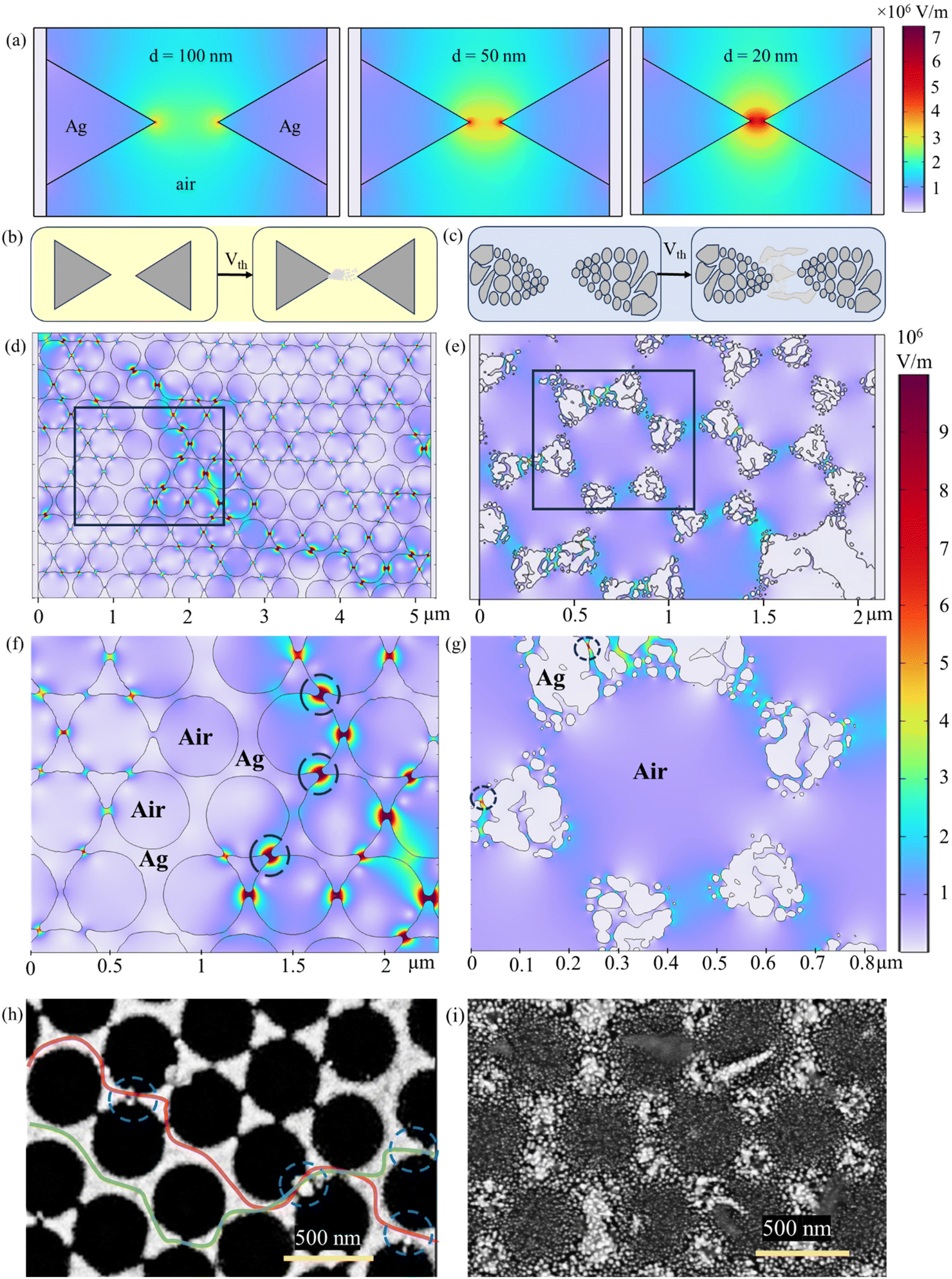 | ||
| Fig. 6 (a) COMSOL Multiphysics simulation to obtain electric field distribution for Ag bowtie structures with different nanogaps with 0.5 V applied on the left Al electrode. Schematic of threshold switching mechanism of devices with (b) triangular and (c) QT structures. Simulated electric field distribution of (d) Ag triangular nanostructure and (e) QT structure. (f) The magnified image of the marked area in (d), shows the hot spots depicting possible paths for filament formation driven by the maximum field intensity, and (g) the marked region in (e), shows the maximum field distribution within the Ag nanoclusters (blue dashed circle). Post-pulsing SEM image showing (h) traces of filaments (red line – path 1, and green line – path 2) across nanogaps (blue dashed circles) of triangular Ag structures and (i) electromigration in random directions of QT structure, which deteriorates its original structure. Note: voltages of 0.5 and 1 V were applied to devices with triangular and QT nanostructure, respectively. | ||
Thus, the present investigation illustrates an approach to desirably confine filaments in planar neuromorphic devices featuring a hierarchical network structure, enhancing performance and achieve computing with minimal energy consumption. The prospective study will focus on investigating the plasmonic effect in conjunction with neuromorphic properties while concurrently exploring the feasibility of utilizing both light and electrical stimuli.
Conclusions
In summary, we have successfully fabricated a planar neuromorphic device with a periodic Ag nanostructure featuring a controllable gap achieved through plasma assisted NSL. Perhaps this would be the first instance of using NSL for neuromorphic device fabrication. For a comparative analysis, we obtained I–V characteristics for multiple devices with varying gaps controlled via OPT for different durations. The device with the minimum gap of 15 nm demonstrates an ultra-low Vth of ∼300 mV, resulting in minimal energy consumption of 8.4 fJ per synapse, comparable to that of a biological synapse. Moreover, the memory and learning behavior of these devices were showcased through appropriate pulsing stimuli, mimicking biological synapses. Notably, the device with the smallest gap exhibits a STP to LTP transition below the microampere range, outperforming many reported literature cases, thanks to the unique geometry of the Ag nanostructure obtained via NSL. Additionally, the psychological behavior of the brain was successfully emulated in an associative learning experiment by employing appropriate pulsing to associate a conditioned (bell) stimulus with an unconditioned one (food). Mechanistically, COMSOL simulation revealed an electric field enhancement across the nanogap between the triangular structures, which confines filament formation between the gaps, thereby reducing energy consumption. This insight was empirically verified through FESEM imaging, illustrating traces of the percolation path aligning with the direction of the electric field. Thus, the present study makes a significant contribution toward low power-consuming neuromorphic devices by utilizing a hierarchical network geometry featuring plasmonic nanostructures.Author contributions
Shubham K. Mehta: investigation, methodology, formal analysis, software, writing – original draft; Indrajit Mondal: conceptualization, investigation, validation, data curation, writing – review and editing; Bhupesh Yadav: investigation, methodology, writing – review and editing; Giridhar U. Kulkarni: conceptualization, data curation, formal analysis, project administration, resources, supervision, writing – review & editing. All authors have approved the final version of the manuscript.Data availability
The data supporting this article have been included as part of the ESI.†Conflicts of interest
There are no conflicts to declare.Acknowledgements
The authors acknowledge the Department of Science and Technology (DST), India, for the funding. The authors thank JNCASR for the facilities. SKM and GUK acknowledge the INSPIRE fellowship, DST, and J.C. Bose fellowship from SERB, India, respectively.References
- G. Lee, J. H. Baek, F. Ren, S. J. Pearton, G. H. Lee and J. Kim, Small, 2021, 17, e2100640 CrossRef PubMed.
- S. Jiang, S. Nie, Y. He, R. Liu, C. Chen and Q. Wan, Mater. Today Nano, 2019, 8, 100059 CrossRef.
- X. B. Yin, Z. H. Tan, R. Yang and X. Guo, J. Electroceram., 2017, 39, 210–222 CrossRef CAS.
- T. Yu, Y. Fang, X. Chen, M. Liu, D. Wang, S. Liu, W. Lei, H. Jiang, S. Shafie, M. N. Mohtar, L. Pan and Z. Zhao, Mater. Horiz., 2023, 10, 2181–2190 RSC.
- D. Xie, Y. Li, J. He and J. Jiang, Sci. China Mater., 2023, 66, 4814–4824 CrossRef CAS.
- Z. Huang, Y. Li, Y. Zhang, J. Chen, J. He and J. Jiang, Int. J. Extreme Manuf., 2024, 6, 032003 CrossRef.
- S. La Barbera, D. Vuillaume and F. Alibart, ACS Nano, 2015, 9, 941–949 CrossRef CAS PubMed.
- T. Masquelier, R. Guyonneau and S. J. Thorpe, Neural Comput., 2009, 21, 1259–1276 CrossRef PubMed.
- M. Prezioso, M. R. Mahmoodi, F. M. Bayat, H. Nili, H. Kim, A. Vincent and D. B. Strukov, Nat. Commun., 2018, 9, 5311 CrossRef CAS PubMed.
- A. Kurenkov, S. Fukami and H. Ohno, J. Appl. Phys., 2020, 128, 010902 CrossRef CAS.
- J. Park, H. Ryu and S. Kim, Sci. Rep., 2021, 11, 16601 CrossRef CAS PubMed.
- Z. Wang, S. Joshi, S. E. Savel'ev, H. Jiang, R. Midya, P. Lin, M. Hu, N. Ge, J. P. Strachan, Z. Li, Q. Wu, M. Barnell, G. L. Li, H. L. Xin, R. S. Williams, Q. Xia and J. J. Yang, Nat. Mater., 2017, 16, 101–108 CrossRef CAS PubMed.
- J. Li, H. Abbas, D. S. Ang, A. Ali and X. Ju, Nanoscale Horiz., 2023, 8, 1456–1484 RSC.
- T. Shi, R. Wang, Z. Wu, Y. Sun, J. An and Q. Liu, Small Struct., 2021, 2, 2000109 CrossRef.
- R. Yang, Chin. Phys. B, 2020, 29, 097305 CrossRef CAS.
- M. Li, H. Liu, R. Zhao, F. S. Yang, M. Chen, Y. Zhuo, C. Zhou, H. Wang, Y. F. Lin and J. J. Yang, Nat. Electron., 2023, 6, 491–505 CrossRef CAS.
- D. P. Sahu and S. N. Jammalamadaka, Sci. Rep., 2817, 7, 17224 CrossRef PubMed.
- Y. Sun, J. Li, S. Li, Y. Jiang, E. Wan, J. Zhang, Y. Shi and L. Pan, Chip, 2023, 2, 100031 CrossRef.
- S. Oh, H. Kim, S. E. Kim, M. H. Kim, H. L. Park and S. H. Lee, Adv. Intell. Syst., 2023, 5, 2200272 CrossRef.
- G. Milano, M. Aono, L. Boarino, U. Celano, T. Hasegawa, M. Kozicki, S. Majumdar, M. Menghini, E. Miranda, C. Ricciardi, S. Tappertzhofen, K. Terabe and I. Valov, Adv. Mater., 2022, 34, 2201248 CrossRef CAS PubMed.
- K. D. M. Rao, A. A. Sagade, R. John, T. Pradeep and G. U. Kulkarni, Adv. Electron. Mater., 2016, 2, 1500286 CrossRef.
- Q. Xia, M. D. Pickett, J. J. Yang, X. Li, W. Wu, G. Medeiros-Ribeiro and R. S. Williams, Adv. Funct. Mater., 2011, 21, 2660–2665 CrossRef CAS.
- M. Kawakita, K. Okabe and T. Kimura, Appl. Phys. Lett., 2016, 108, 023101 CrossRef.
- S. K. Bose, J. B. Mallinson, R. M. Gazoni and S. A. Brown, IEEE Trans. Electron Devices, 2017, 64, 5194–5201 CAS.
- K. Sakai, T. Sato, S. Tani, M. Ito, M. Yagi and J. I. Shirakashi, AIP Adv., 2019, 9, 055317 CrossRef.
- S. K. Bose, S. Shirai, J. B. Mallinson and S. A. Brown, Faraday Discuss., 2019, 213, 471–485 RSC.
- A. Gee, A. H. Jaafar and N. T. Kemp, Nanotechnology, 2020, 31, 155203 CrossRef CAS PubMed.
- S. Liu, X. Zhong, Y. Li, B. Guo, Z. He, Z. Wu, S. Liu, Y. Guo, X. Shi, W. Chen, H. Duan, J. Zeng and G. Liu, Adv. Sci., 2023, 35, 2212118 Search PubMed.
- S. Liu, J. Zeng, Z. Wu, H. Hu, A. Xu, X. Huang, W. Chen, Q. Chen, Z. Yu, Y. Zhao, R. Wang, T. Han, C. Li, P. Gao, H. Kim, S. J. Baik, R. Zhang, Z. Zhang, P. Zhou and G. Liu, Nat. Commun., 2023, 14, 7655 CrossRef CAS PubMed.
- B. Bannur and G. U. Kulkarni, Mater. Horiz., 2020, 7, 2970–2977 RSC.
- R. Attri, I. Mondal, B. Yadav, G. U. Kulkarni and C. N. R. Rao, Mater. Horiz., 2023, 11, 737–746 RSC.
- B. Bannur, B. Yadav and G. U. Kulkarni, ACS Appl. Electron. Mater., 2022, 4, 1552–1557 CrossRef CAS.
- T. S. Rao, I. Mondal, B. Bannur and G. U. Kulkarni, Discover Nano, 2023, 18, 124 CrossRef PubMed.
- B. Yadav, I. Mondal, B. Bannur and G. U. Kulkarni, Nanotechnology, 2024, 35, 015205 CrossRef PubMed.
- D. Xie, G. Gao, B. Tian, Z. Shu, H. Duan, W. W. Zhao, J. He and J. Jiang, Adv. Mater., 2023, 35, 2212118 CrossRef CAS PubMed.
- N. Ilyas, J. Wang, C. Li, D. Li, H. Fu, D. Gu, X. Jiang, F. Liu, Y. Jiang and W. Li, Adv. Funct. Mater., 2022, 32, 2110976 CrossRef CAS.
- C. L. Haynes and R. P. Van Duyne, J. Phys. Chem. B, 2001, 105, 5599–5611 CrossRef CAS.
- M. Domonkos and A. Kromka, Symmetry, 2022, 14, 2642 CrossRef CAS.
- P. Colson, C. Henrist and R. Cloots, J. Nanomater., 2013, 2013, 948510 CrossRef.
- X. Zhang, C. R. Yonzon and R. P. Van Duyne, J. Mater. Res., 2006, 21, 1083–1092 CrossRef CAS.
- L. Li, F. Du, X. Zong, L. Cui and Y. Liu, Appl. Opt., 2022, 61, 6924 CrossRef CAS PubMed.
- M. Pisco, F. Galeotti, G. Quero, G. Grisci, A. Micco, L. V. Mercaldo, P. D. Veneri, A. Cutolo and A. Cusano, Light: Sci. Appl., 2017, 6, 16229 CrossRef PubMed.
- T. Qiu, E. M. Akinoglu, B. Luo, M. Konarova, J. H. Yun, I. R. Gentle and L. Wang, Adv. Mater., 2022, 34, e2103842 CrossRef PubMed.
- S. Huang, Q. Yang, C. Zhang, L. Kong, S. Li and J. Kang, Thin Solid Films, 2013, 536, 136–141 CrossRef CAS.
- D. Ji, T. Li and H. Fuchs, Adv. Electron. Mater., 2017, 3, 1600348 CrossRef.
- A. A. Osipov, A. E. Gagaeva, A. B. Speshilova, E. V. Endiiarova, P. G. Bespalova, A. A. Osipov, I. A. Belyanov, K. S. Tyurikov, I. A. Tyurikova and S. E. Alexandrov, Sci. Rep., 2023, 13, 3350 CrossRef CAS PubMed.
- Y. Chen, D. Shi, Y. Chen, X. Chen, J. Gao, N. Zhao and C. P. Wong, Nanomaterials, 2019, 9, 605 CrossRef CAS PubMed.
- Y. C. Chang, S. M. Wang, H. C. Chung, C. Bin Tseng and S. H. Chang, Plasmonics, 2011, 6, 599–604 CrossRef CAS.
- K. Schraml, M. Spiegl, M. Kammerlocher, G. Bracher, J. Bartl, T. Campbell, J. J. Finley and M. Kaniber, Phys. Rev. B: Condens. Matter Mater. Phys., 2014, 90, 035435 CrossRef CAS.
- J. Tang, F. Yuan, X. Shen, Z. Wang, M. Rao, Y. He, Y. Sun, X. Li, W. Zhang, Y. Li, B. Gao, H. Qian, G. Bi, S. Song, J. J. Yang and H. Wu, Adv. Mater., 2019, 31, 1902761 CrossRef CAS PubMed.
- D. P. Sahu, K. Park, J. Han and T. S. Yoon, APL Mater., 2022, 10, 051111 CrossRef CAS.
- F. Ahmed, M. S. Choi, X. Liu and W. J. Yoo, Nanoscale, 2015, 7, 9222–9228 RSC.
- S. Misra, L. C. Bland, S. G. Cardwell, J. A. C. Incorvia, C. D. James, A. D. Kent, C. D. Schuman, J. D. Smith and J. B. Aimone, Adv. Mater., 2023, 35, 2204569 CrossRef CAS PubMed.
- S. T. Keene, A. Melianas, Y. van de Burgt and A. Salleo, Adv. Electron. Mater., 2019, 5, 1800686 CrossRef.
- H. Masuda and T. Kizuka, J. Nanosci. Nanotechnol., 2014, 14, 2436–2440 CrossRef CAS PubMed.
- M. F. Abd Alameer and T. H. Khalaf, IOP Conf. Ser.: Mater. Sci. Eng., 2020, 757, 012018 CrossRef.
Footnote |
| † Electronic supplementary information (ESI) available. See DOI: https://doi.org/10.1039/d4nr02748e |
| This journal is © The Royal Society of Chemistry 2024 |