
Highly stable two-dimensional Ruddlesden–Popper perovskite-based resistive switching memory devices†
Milon
Kundar‡
ab,
Koushik
Gayen‡
ab,
Rajeev
Ray
ab,
Dushyant
Kushavah
 ab and
Suman Kalyan
Pal
*ab
ab and
Suman Kalyan
Pal
*ab
aSchool of Physical Sciences, India Institute of Technology Mandi, Kamand, Mandi-175005, Himachal Pradesh, India. E-mail: suman@iitmandi.ac.in; Tel: +91 1905 267040
bAdvanced Materials Research Centre, India Institute of Technology Mandi, Kamand, Mandi-175005, Himachal Pradesh, India
First published on 29th July 2024
Abstract
Resistive switching random-access memory (ReRAM) devices based on organic–inorganic halide perovskites (OIHPs) have emerged as a new class of data storage devices. Recently, two-dimensional (2D) OIHPs have attracted much attention for ReRAM applications because of their structural diversity and superior stability. Here, the RS characteristics of ReRAM devices fabricated utilizing pure 2D Ruddlesden–Popper (RP) perovskite crystals, namely (TEA)2PbBr4 and (TEA)2PbI4, are reported. The RS memory devices exhibit reliable and reproducible bipolar switching properties with high ON/OFF ratio (∼104), excellent data retention of over 104 s, and good endurance characteristics of 200 cycles. This study investigates temperature-dependent RS behaviors, elucidating the creation and annihilation of a conducting pathway in the presence of an external electric field. Additionally, the RS property of 2D RP perovskite-based memory devices is found to be retained over 45 days at ambient conditions under a relative humidity of 47% ± 4%. Our findings may accelerate the technological deployment of stable 2D perovskite-based RS memory devices for successful logic application.
1. Introduction
Organic–inorganic halide perovskites (OIHPs) have had a remarkable influence on solar-cell development owing to their superior properties, such as strong optical absorption, low exciton binding energy, tunable bandgap, long charge-diffusion length, and high charge-carrier mobility.1–5 However, the current–voltage (I–V) hysteresis induced by ion or defect migration in the OIHP layer has expanded their applications in resistive switching (RS) memory and artificial synapses.6–8 Over the last couple of years, OIHPs have stimulated research interest in resistive switching random-access memory (ReRAM) devices due to their high switching speed with multilevel data storage capability, flexibility, and low operating voltages.9–11 Besides these attributes, their low cost and solution processability have made OIHPs more competitive among the materials of the RS memory devices industry.12 Three-dimensional (3D) OIHPs, such as MAPbI3 and FAPbI3, have been mostly investigated for perovskite resistive memory (PRM) devices. These PRM devices exhibit high ON/OFF ratios, multilevel switching, and low power consumption.9,13,14 A wide range of materials, including binary oxides, polymers, transition metal dichalcogenides, perovskites, and organic compounds, have demonstrated RS characteristics.15 Although oxides are the most widely studied materials for RS memories, their performance in ReRAM is compromised by the necessity of high power consumption, under vacuum conditions, and high-temperature processing.14 Alternatively, OIHP materials have emerged as promising candidates for memory devices due to their low current leakage, mixed ionic–electronic conduction, and tuneable band gap.16 However, 3D halide perovskites face challenges with their photo-, humid, and thermal stability compared to conventional ReRAM devices based on metal oxides, leading to degradation in the performance of OIHP-based memory devices.17–19Recently, two-dimensional (2D) Ruddlesden–Popper (RP) perovskites have shown promise for use in optoelectronic devices, because 2D perovskites with long organic spacers possess more structural diversity and intrinsic stability.20 Nonetheless, 2D perovskites naturally form quantum-well structures with inorganic sheets as wells and large organic layers as barriers. The hydrophobic nature of bulky organic spacers in 2D RP perovskites can prevent PRM devices from breaking down and also protect the inorganic layers from humid and ambient atmospheres.21–24 This stability development is crucial for the steady switching operation of RS memory devices. In a typical ReRAM device, the active layer may be electrically switched between a low resistance state (LRS) and a high resistance state (HRS) to store information by applying various voltage amplitudes or polarity. The main reason for the resistive switching in PRM devices has been considered to be the formation/rupture of a conductive filament owing to defect migration.25
Normally, the bandgap of 2D OIHPs is wider than that of 3D due to the presence of large organic cations in their structures.26,27 The wide bandgap of 2D perovskites can make the Schottky barrier much higher at the perovskite–electrode interface and can lower the HRS current of PRM devices, resulting in a greater ON/OFF ratio.28 Moreover, due to the isolated configuration of octahedral complexes due to the spacer cation, the transport of charge carriers is limited in the 2D plane, leading to the high intrinsic resistivity. This characteristic proves advantageous in ReRAM applications as it enables easier reduction of the OFF current and consequently amplifies the ON/OFF ratio.29 More importantly, halide vacancies are the crucial factors for hybrid halide perovskite-based memory devices. In wider bandgap OIHPs, the interaction energy between halide vacancies is low. This lower interaction energy facilitates the formation and rupture of halide vacancies in conductive filaments, valuable for high ON/OFF ratios.30 Seo et al. fabricated ReRAM devices based on 2D (BA)2PbI4 (BA = butylammonium) perovskites.31 They demonstrated that 2D memory devices possess lower operating fields, greater ON/OFF ratios, and significantly more stable endurance than 3D devices. According to them, the higher thermal activation energy and Schottky barrier of 2D perovskites are responsible for the improved RS features of 2D PRM cells. However, reports on pure 2D perovskite-based memory devices are limited and more studies are required to understand the RS mechanism in 2D PRM devices.
In our study, (TEA)2PbBr4 [TEA = 2-thiopheneethylammonium] and (TEA)2PbI4 2D perovskites are synthesized and employed individually as the RS elements in an ReRAM cell to compare the dependence of RS behavior on Br and I. The PRM devices with an ITO/(TEA)2PbBr4 or a (TEA)2PbI4/Al structure exhibit good electrical characteristics, including low voltage operation, consistent data retention, and highly stable endurance. The RS mechanism is rationalized by the formation and rupture of conductive filaments of both halide vacancies and Al ions in 2D perovskites. Moreover, we demonstrate long-term stability in 2D PRM devices, especially in (TEA)2PbBr4-based memory devices under ambient conditions.
2. Experimental section
2.1 Materials
2-Thiopheneethylamine (TEA, 98%), lead(II) bromide (PbBr2, 99.999%, metals basis), isopropyl alcohol, lead iodide (PbI2, 99.999%, metals basis), dimethylformamide (DMF), hydroiodic acid (HI, 57%), dimethyl sulfoxide (DMSO), hydrobromic acid (HBr, 48%), octylamine, toluene, and oleic acid were purchased from Sigma Aldrich. All of these ingredients were utilized without additional purification.2.2 Synthesis of perovskite crystals and device fabrication
The (TEA)2PbBr4 and (TEA)2PbI4 perovskite crystals were synthesized following our previous works.32,33 In brief, we dissolved 0.2 mmol of TEABr and 0.1 mmol of PbBr2 in stoichiometric ratio in 250 μL of DMF with 0.16 mmol octylamine and 0.16 mmol oleic acid to obtain a precursor solution. Then, 5 mL of toluene was promptly added into the precursor solution while stirring. After centrifuging the mixture at 5000 rpm for 50 s, the precipitated (TEA)2PbBr4 perovskite was obtained. We synthesized (TEA)2PbI4 perovskite crystals following the same procedure using TEAI and PbI2. The (TEA)2PbBr4 and (TEA)2PbI4 crystals were moved into a glove box and heated at 60 °C overnight on a hot plate. This resulted in white (TEA)2PbBr4 and yellow (TEA)2PbI4 perovskite powders (Fig. S1†). Finally, 110 mg of each 2D perovskite crystal was individually redispersed in 1 mL of toluene for further use (Fig. S1†). For fabrication of PRM devices, ITO-coated glass substrates were cleaned with detergent water, deionized (DI) water, acetone, and isopropyl alcohol (IPA) in an ultrasonic bath sequentially for 30 min, and then exposed to UV/ozone for 20 min in a UV-ozone chamber. 2D perovskite films were prepared by spin casting the (TEA)2PbBr4/(TEA)2PbI4 perovskite solution (in toluene) onto the ITO substrates at 3000 rpm for 30 s and annealing at 70 °C for 10 min. Finally, Al electrodes of 70 nm thickness were deposited on top of the 2D perovskite films by means of a thermal evaporating system (from Excel Instruments) under a high vacuum (<5 × 10⁻⁶ mbar) through a shadow mask.2.3 Characterization
The surface and cross-sectional field-emission scanning electron microscopy (FESEM) images of the 2D perovskite films were captured using an FEI Nova Nano SEM-450 tool. Steady-state photoluminescence (PL) and UV-visible absorption spectra were respectively recorded using HORIBA Fluorolog-3 and Shimadzu UV-2450 spectrometers. An atomic force microscopy (AFM) system (Dimension Icon from Bruker) was used to measure the roughness of the perovskite films. X-ray diffraction (XRD) patterns of the (TEA)2PbBr4 and (TEA)2PbI4 perovskite films were acquired by utilizing a Rigaku Smart Lab 9 kW rotating anode diffractometer. The electrical properties of the fabricated ReRAM devices were measured using a Keithley 2400 source meter.3. Results and discussion
Initially, 2D RP perovskite crystals (TEA)2PbBr4 and (TEA)2PbI4 were synthesized (see Experimental section). To investigate the surface morphology of (TEA)2PbBr4 and (TEA)2PbI4 perovskite layers, scanning electron microscopy (SEM) procedures were performed. The top-view SEM images of the perovskite films are shown in Fig. 1. It is clear from these SEM images that the (TEA)2PbI4-coated film exhibits a larger crystal domain compared to the (TEA)2PbBr4 film. The thickness of the (TEA)2PbBr4 and (TEA)2PbI4 layers was estimated from the cross-sectional SEM images displayed in Fig. 1c, which reveal a thickness of approximately 200 nm for both films. The surface roughness of the (TEA)2PbBr4 and (TEA)2PbI4 perovskite layers were investigated by atomic force microscopy (AFM), as shown in Fig. S2.† It is observed that the root-mean-square (RMS) values of roughness for the (TEA)2PbBr4 and (TEA)2PbI4 perovskite films are 35.7 and 30.3 nm, respectively. XRD measurements of perovskite films were conducted to identify the crystal structure. Fig. 1d shows XRD patterns of the (TEA)2PbBr4 and (TEA)2PbI4 films. The (TEA)2PbBr4 and (TEA)2PbI4 perovskite films exhibit low-angle diffraction peaks at ≈6.03° and ≈5.96°, respectively, indicating the formation of 2D crystal structures in the films.34 Fig. S3† shows the enlarged view of low-angle peaks for both perovskite films. The shift in low-angle XRD peak of (TEA)2PbBr4 from that of (TEA)2PbI4 may be ascribed to the variation of halide atom. The unit cell in a 2D frame reduces or expands as the ionic radius of the halide atom changes, causing a shift in the associated XRD peak.35 Consequently, we studied the optical properties of (TEA)2PbBr4 and (TEA)2PbI4 perovskites by recording the absorption and PL spectra. Fig. 1e displays the absorption spectra of the (TEA)2PbBr4 and (TEA)2PbI4 perovskites in the solid state.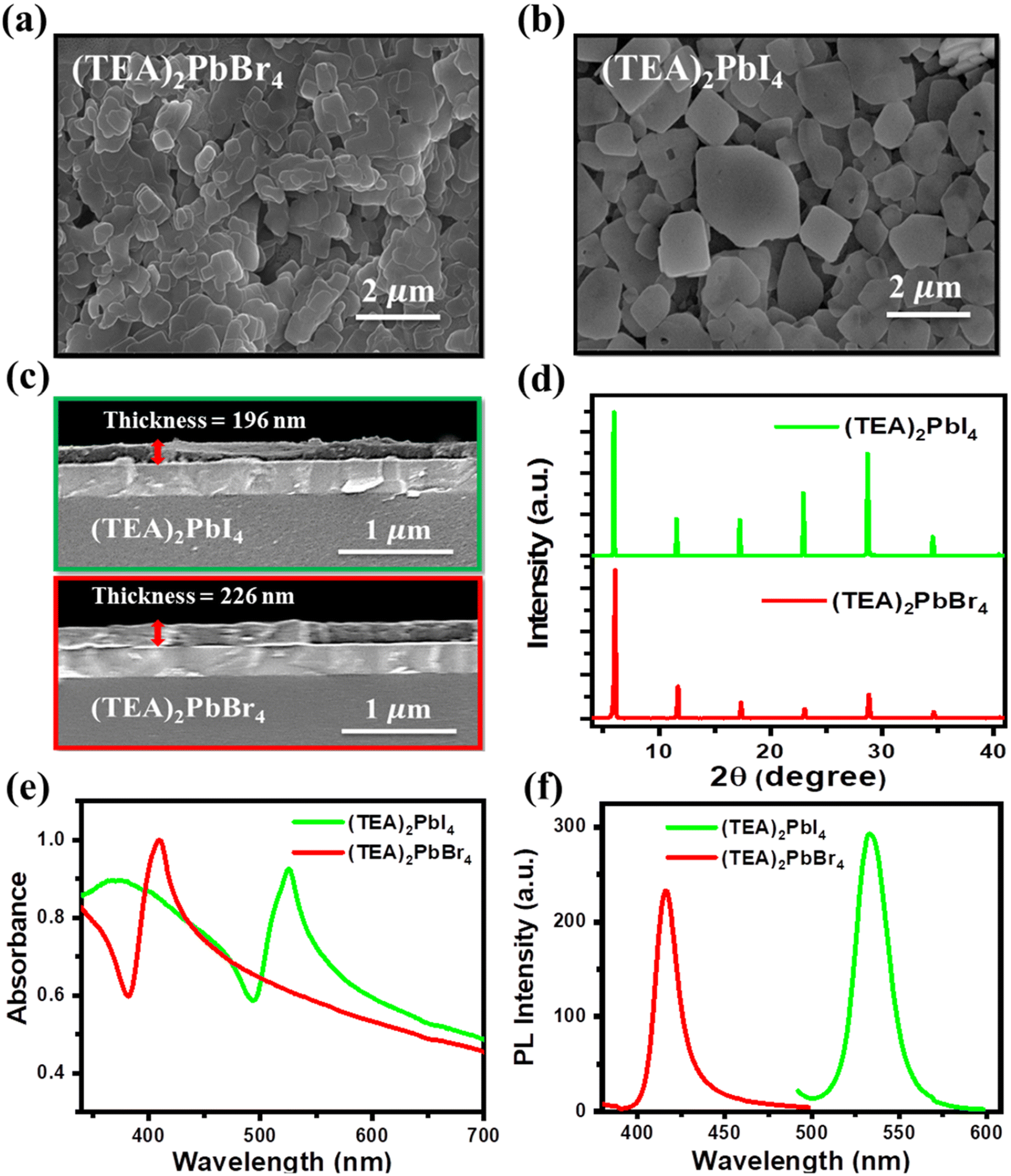 | ||
| Fig. 1 Top-view SEM images of (a) (TEA)2PbBr4 and (b) (TEA)2PbI4 perovskites. (c) Cross-sectional SEM images, (d) XRD patterns, (e) UV-vis absorption spectra, and (f) PL spectra of (TEA)2PbBr4 and (TEA)2PbI4 perovskite films. | ||
The absorption peak of (TEA)2PbBr4 is located at 409 nm (3.03 eV), while (TEA)2PbI4 shows a red-shifted absorption peak at 526 nm (2.36 eV). The PL peaks for the (TEA)2PbBr4 and (TEA)2PbI4 films are centered at 416 nm (2.98 eV) and 533 nm (2.33 eV), respectively (Fig. 1f). When the halide component of a perovskite is changed from Br to I, a significant red shift of PL has previously been observed.32 This change in the bandgap has been ascribed to variation in the lattice constant related to distinct halide compositions, alongside change in the electronegativity that modifies the band structure.36
Fig. 2a illustrates a schematic structure of the ReRAM device, featuring the vertical stack of Al electrode/(TEA)2PbI4 layer/ITO bottom electrode. A similar device structured with a (TEA)2PbBr4 perovskite layer is shown in Fig. S4a.† The choice of Al as an electrode in PRM devices is motivated by several factors. In electrochemical metallization (ECM), a resistance change is induced by conducting filaments formed from an electrochemically active metal electrode, such as Ag or Al. When an electric field is applied to the cell, the electrochemically active metal on the top electrode undergoes oxidation and migrates to the bottom electrode, where the cation is reduced to form conducting filaments within the active layer.38 Additionally, Al metal exhibits high conductivity with a relatively low work function and undergoes rapid oxidation due to its low Gibbs free energy.37 In contrast, inert metals, like Au, have a low oxygen affinity, which prevents them from chemically reacting with the device's active layer.37 In our previous work, the energetic positions of conduction and valence bands of the (TEA)2PbBr4 and (TEA)2PbI4 perovskites were determined through ultraviolet photoelectron spectroscopy (UPS) and optical band gap measurements.32 The energy level diagrams showing the energy levels of each component (using the values reported in ref. 32) in the memory devices are presented in Fig. 2b and Fig. S4b.† The (TEA)2PbBr4 and (TEA)2PbI4 2D perovskites show a wider bandgap, which makes the Schottky barrier much higher at the interface between Al top electrodes and the perovskite layer. It is well known that the current flow in the HRS is correlated with the height of the Schottky barrier. The increased Schottky barrier height of 2D perovskites lowers the HRS current, which can lead to increase of the ON/OFF ratio in PRM devices.28
 | ||
| Fig. 2 (a) Schematic illustration of the (TEA)2PbI4 PRM device structure showing the 2D perovskite layer. (b) Band alignment with the energy levels of every component in the device. (c) Typical I–V curves of (TEA)2PbBr4 and (TEA)2PbI4 PRM devices. Statistically analyzed SET and RESET voltages for 200 cycles of one (d) (TEA)2PbBr4- and (e) (TEA)2PbI4-based device. | ||
To explore the switching behaviors of (TEA)2PbBr4- and (TEA)2PbI4-based memory devices, the I–V characteristics of the cells were measured under the voltage sweep at 0 V → +3 V → 0 V → −3 V → 0 V. To avoid irreversible device breakdown during the electroforming process, a constant compliance current of 0.1 A was maintained along with the applied voltage ranging from −3 V to +3 V. Fig. 2c presents typical I–V curves of (TEA)2PbBr4- and (TEA)2PbI4-based PRM devices. These I–V hysteresis loops demonstrate that the 2D perovskite-based devices exhibit bipolar resistive switching (RS), implying that the ON/OFF switching of the device occurred at opposite polarities. It should be noted that the I–V curves are not symmetric under positive and negative voltages. The asymmetry in the I–V characteristics in PRM devices can arise from inherent material properties and structural asymmetries. The I–V curve of ReRAM devices can exhibit asymmetry due to inhomogeneous defects, resulting in a non-uniform current distribution.39 Additionally, discrepancies in electrical behaviors between forward and reverse bias conditions may occur at the interfaces between the perovskite layer and the electrodes due to the different work functions of the bottom and top electrodes.37 The RS mechanism is governed by the SET and RESET processes. Initially, the device is in the HRS or insulating state, but at a certain positive voltage, the current increases abruptly and the device reaches an LRS. This switching from an HRS (OFF state) to LRS (ON state) is known as the SET process. Similarly, at a certain negative voltage, the state of the device changes from LRS to HRS, which is termed as the RESET process. It is evident from Fig. 2c that during the positive voltage scan from 0 to 3 to 0 V, the (TEA)2PbBr4 device switches from HRS to LRS at 0.34 V (SET voltage) with an abrupt dropping of resistance. The PRM is returned from LRS to HRS at −2.09 V (RESET voltage) during the negative sweep from 0 to −3 to 0 V. Similarly, the (TEA)2PbI4 device shows RS with SET and RESET voltages of 0.28 and −1.97 V, respectively. Fig. 2d displays the SET and RESET voltages during 200 cycles of operation of one mother device of (TEA)2PbBr4 perovskite. There is a variation in SET (0.15 to 0.33 V) and RESET (−1.73 to −2.34 V) voltages of the (TEA)2PbBr4 device. Similarly, a (TEA)2PbI4-based PRM device exhibits fluctuations in both SET (0.21 to 0.34 V) and RESET (−1.73 to −2.16 V) voltages, as depicted in Fig. 2e. Several studies reported that the rate of vacancy migration in perovskite materials is predominantly influenced by the associated activation energy.40 The activation energy of vacancy migration of bromine is lower than that of iodine, potentially facilitating the migration of bromine vacancies towards the electrode, leading to the formation of a conductive pathway within the perovskite film.41 As a result, the SET electric field of PRM devices fabricated with (TEA)2PbBr4 is lower compared to that of (TEA)2PbI4-based devices. In Fig. S5,† the distributions of SET and RESET voltages of 10 different devices are presented to assess the operational consistency of (TEA)2PbBr4- and (TEA)2PbI4-based memory devices. Interestingly, no appreciable difference in RS behavior in terms of SET and RESET voltages is found between those ReRAM devices. Such small variations in SET and RESET voltages suggest that the RS is reproducible in PRM devices.
Switching endurance is also one of the important factors that influences the reliability of PRM devices. We measured the endurance characteristics of (TEA)2PbBr4 and (TEA)2PbI4 memory devices and the results are presented in Fig. 3(a and b). During the endurance test, the memory cells were operated at −0.5 V for the SET and RESET processes. Both the devices were functional for 200 endurance cycles. The average values of HRS and LRS of the (TEA)2PbBr4 PRM are estimated to be 1.23 × 10⁵ and 41 Ω, respectively, leading to an ON/OFF ratio of 3 × 10³. However, the (TEA)2PbI4 device exhibits average HRS and LRS values of 3.53 × 10⁵ and 40 Ω, respectively, with an ON/OFF ratio of 8.83 × 10³. Nonetheless, consistent RS behavior without any significant degradation of HRS and LRS has been observed over the 200 cycles of operation. To study the electrical reliability of the 2D perovskite-based memory devices, the data retention of the OFF and ON states was assessed. Fig. 3(c and d) depicts the retention time of LRS and HRS recorded at a reading voltage of −0.5 V with an interval of 30 s. A consistent ON/OFF ratio is observed for both perovskite-based ReRAMs over 104 s. From our results, it can be inferred that (TEA)2PbBr4- and (TEA)2PbI4-based ReRAMs exhibit high operational reliability and reproducibility.
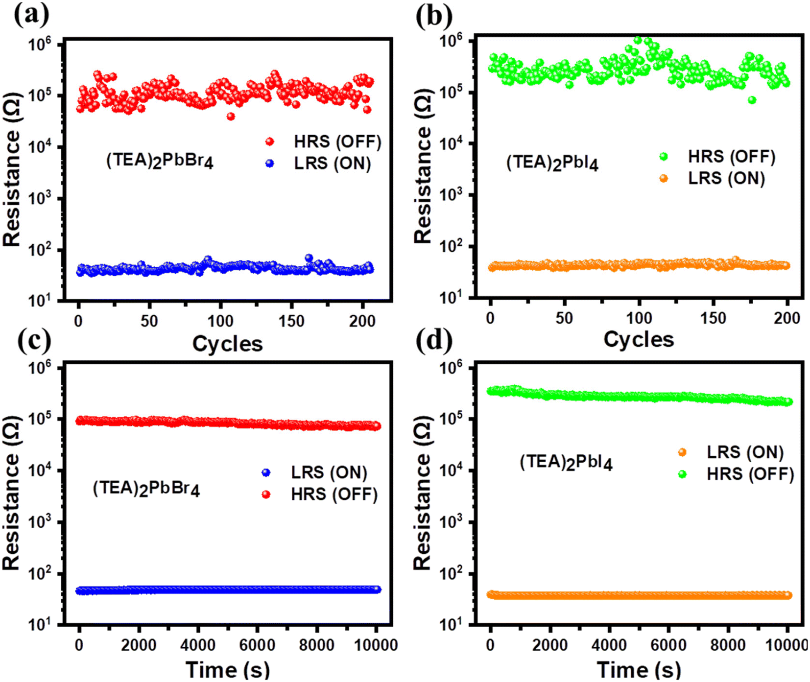 | ||
| Fig. 3 Endurance characteristics of (a) (TEA)2PbBr4 and (b) (TEA)2PbI4 PRM devices over 200 cycles. Retention properties of the ON and OFF states for (c) (TEA)2PbBr4 and (d) (TEA)2PbI4 cells. | ||
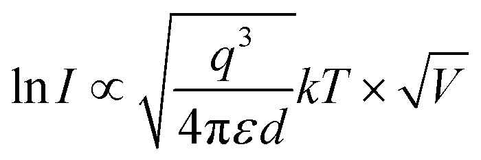
To understand the conduction mechanisms of PRM devices, the I–V curve corresponding to the SET operation was replotted on a double-logarithmic scale. Fig. 4(a and b) displays ln(I) vs. ln(V) plots for the SET process of (TEA)2PbBr4 and (TEA)2PbI4 devices. The slope of the curves in the LRS are 1.01 and 1 for (TEA)2PbBr4 and (TEA)2PbI4, respectively (Fig. 4(c and d)). The near-unity values of the fitted slopes for both samples suggest that the main conduction mechanism in the LRS correlates with ohmic-like conduction, indicating a well-formed conducting filament during the SET process.14,42–44 This observation implies that ohmic conduction dominates in the LRS after the conducting filament is abruptly formed in the perovskite layer. On the other hand, the ln![[thin space (1/6-em)]](https://www.rsc.org/images/entities/char_2009.gif) I–lnV curves in the HRS exhibited two distinct slopes at lower and higher voltage regions (Fig. 4(a and b)). In the low voltage region (<0.16 V for (TEA)2PbBr4 and <0.22 V for (TEA)2PbI4 devices), the I–V characteristic in the HRS follows Ohm's law. Conversely, above 0.2 V, the slopes of the curves for (TEA)2PbBr4 and (TEA)2PbI4 in the HRS are 1.93 and 2.03, respectively, indicating deviation from Ohm's law. In the case of Schottky barrier formation, the current should follow the relation:14
I–lnV curves in the HRS exhibited two distinct slopes at lower and higher voltage regions (Fig. 4(a and b)). In the low voltage region (<0.16 V for (TEA)2PbBr4 and <0.22 V for (TEA)2PbI4 devices), the I–V characteristic in the HRS follows Ohm's law. Conversely, above 0.2 V, the slopes of the curves for (TEA)2PbBr4 and (TEA)2PbI4 in the HRS are 1.93 and 2.03, respectively, indicating deviation from Ohm's law. In the case of Schottky barrier formation, the current should follow the relation:14
 | (1) |
I vs. V1/2 in the HRS region (>0.16 V for (TEA)2PbBr4 and >0.22 V for (TEA)2PbI4 devices) as shown in Fig. 4(e and f). The linear correlation between lnI and V1/2 suggests that Schottky conduction is prevalent in the HRS region.
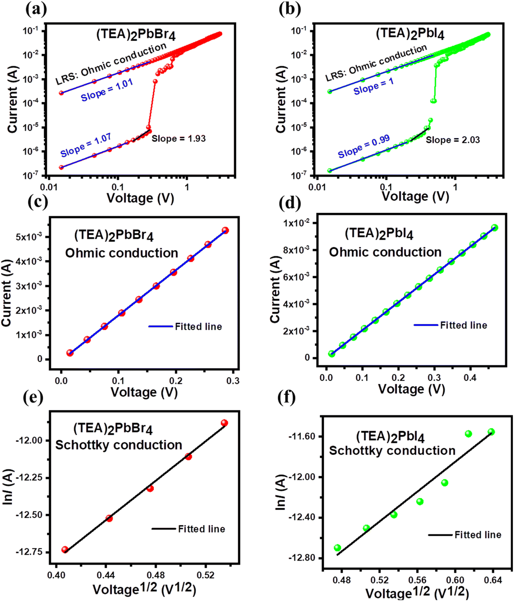 | ||
| Fig. 4 (a and b) Double-logarithmic plots of I–V curves, (c and d) proportional relation between I and V in LRS, and (e and f) lnI–V1/2 plots in the HRS for (TEA)2PbBr4 and (TEA)2PbI4 devices. The straight lines are the results of linear fittings. | ||
To confirm the influence of temperature on the RS behaviors of (TEA)2PbBr4 and (TEA)2PbI4 PRM devices, I–V measurements were carried out across the temperature range of room temperature (298 K)–398 K. Fig. 5(a and b) depicts an increase in the HRS current as temperature rises. The trend of growing current can be ascribed to the variation in the thermally assisted hopping distance within the HRS.7 The distributions of SET and RESET voltages with varying temperatures for (TEA)2PbBr4 and (TEA)2PbI4 devices are shown in Fig. 5(c–f). As the temperature rises, the SET and RESET voltages exhibit a gradual decrease, suggesting that filament formation and rupture become easier at elevated temperatures.45 In the SET processes, the operating voltage can be correlated to the rate of ion migration.
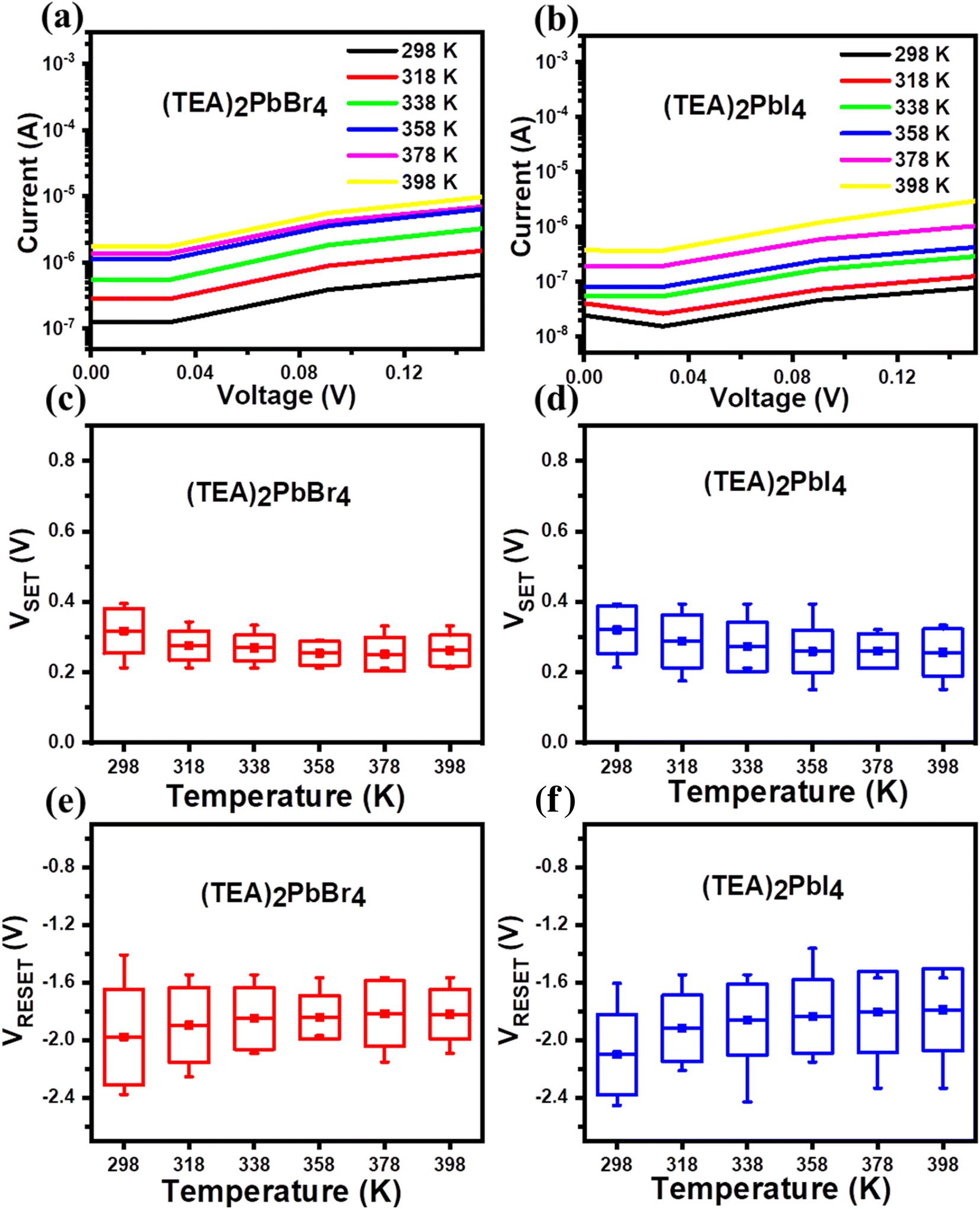 | ||
| Fig. 5 (a and b) Temperature dependence of the I–V characteristics of the HRS before the SET process, (c and d) SET, and (e and f) RESET voltage distributions measured at various temperatures for (TEA)2PbBr4 and (TEA)2PbI4 devices. | ||
In the perovskite materials, the filament formation may partly originate from the creation of extra bromide or iodide vacancies with increasing temperature.46 This phenomenon could potentially allow construction of more robust halide-vacancy-based conducting filaments, even at low SET voltages. On the other hand, during the RESET processes, the conducting filament can rupture due to Joule heating.47,48 Moreover, the narrow conducting filaments are thermally unstable and can easily break at high temperatures. Therefore, filament rupture can occur readily with increasing temperature, even in low electric fields. However, the mechanism of resistive switching in PRM devices is still a topic of debate.49–51
Based on our findings (presented above), it is noteworthy to mention that the valence change mechanism (VCM) could play a key role in controlling the RS mechanism in OIHP-based memory devices.52,53 According to the VCM theory, halide vacancies are responsible for the formation and breakdown of filaments in PRM devices. The RS behavior can be ascribed to the migration of bromine/iodine ions and their corresponding vacancies, facilitated by the low activation energy.54 Initially, in the absence of an electric field, a small amount of I or Br vacancy point defects is randomly distributed in the (TEA)2PbBr4 or (TEA)2PbI4 perovskite layers (Fig. 6a). Thus, the drift of electrons through the central perovskite layer is difficult, resulting in the HRS. Upon applying a positive bias to the PRM device in its HRS, bromine/iodine ions can effortlessly migrate towards the Al top electrode, while corresponding vacancies can accumulate from the bottom to the top electrode as 1D-like channels.55 The gradual increase in the concentration of Br/I ions and their associated vacancies between the perovskite layer and electrodes lowers the contact barrier, leading to enhanced conduction at the interfaces. Once the multifilaments of the vacancy are formed with the increasing positive bias, the PRM device switches from its HRS to LRS (SET process). Thereafter, upon the application of an opposite electric field, there is a disruption in the conduction channel, leading the device to return to its HRS in the RESET process.
 | ||
| Fig. 6 Diagrams explaining the RS mechanism via formation of a conductive filament of (a) halide anions and (b) electrochemically active metal cations. | ||
Besides this, another type of mechanism, known as electrochemical metallization (ECM), may also contribute to the RS behavior in OIHP-based memory devices.56Fig. 6b illustrates a conductive filament formation mechanism based on electrochemically active metal cations. According to the ECM process, when a positive voltage is applied to the top electrode, the Al atom undergoes initial ionization (Al3+) and subsequently propagates towards the counter electrode (ITO) via the ion-hopping mechanism.50 Upon arrival at the ITO electrode, the Al cations are neutralized by acquiring opposite charge carriers. The metal nucleus grows spontaneously above its supersaturation threshold, resulting in the formation of a metal filament between the ITO and counter electrodes.14 Subsequently, the device switches from its HRS to LRS. When a bias is applied in the opposite direction, the filament experiences disruption due to dissolution assisted by Joule heating.57 It is widely accepted that the conduction mechanism in PRM devices depends on the choice of electrodes and perovskite active materials.44 Therefore, the RS mechanism in the fabricated memory device can be ascribed to the synergistic effect of filament formation by Br/I vacancy and Al.
To verify the involvement of Al in the RS process, we performed energy-dispersive spectroscopy (EDS) measurements on a specific cross-sectional region of a (TEA)2PbI4-based device (Fig. S6a†) and analyzed the elemental distributions in this area (Fig. S6b†). The EDS measurement was made immediately after applying a positive voltage sweep to the device. We chose a specific cross-sectional perovskite area of the device where no Al metal electrode was attached. The EDS mapping (Fig. S6b†) confirmed the existence of Al within the perovskite layer. This investigation provides direct evidence of Al ion migration or conduction filament formation through the perovskite layer in the PRM device.
Finally, the long-term environmental stability of PRM devices was investigated by storing the fabricated devices under ambient conditions (air, RH ≈ 47% ± 4%, room temperature in the dark) without encapsulation. Fig. 7(a and b) illustrates the I–V characteristics (measured at different times) of (TEA)2PbBr4- and (TEA)2PbI4-based devices, respectively. It is clear from the figures that the RS behavior of (TEA)2PbBr4 devices remains almost invariant after 45 days, but it changes considerably after 30 days for (TEA)2PbI4 devices. Next, we compared 1-day and 45-day retention of (TEA)2PbBr4 and (TEA)2PbI4 PRM devices, as shown in Fig. S7.† In (TEA)2PbBr4 devices, a slight reduction of the HRS is observed, while the LRS remained almost consistent over the 45 days. However, the (TEA)2PbI4 PRM cell exhibits irregular retention after 30 days. The stable RS behavior of these 2D perovskites could be attributed to the superior hydrophobicity of their spacer cations.58 The hydrophobic TEA cation induces steric hindrance, which influences the surface Pb–Br/Pb–I bond to prevent water adsorption.59 Furthermore, the stacks of hydrophobic TEA layers shield the inner perovskites from moisture and oxygen, thus enhancing the environmental stability of the devices.60 Moreover, (TEA)2PbBr4 PRM cells have shown more stability compared to (TEA)2PbI4 devices (Fig. 7). I-containing perovskite materials tend to undergo oxidation when exposed to air and light.32 The ionic radius of Br (1.96 Å) is smaller than that of I (2.20 Å), resulting in a smaller unit cell volume for TEA2PbBr4 compared to TEA2PbI4. It has been reported that the structural stability resulting from the contraction of the perovskite lattice could be a crucial factor contributing to the improved stability of Br-containing 2D perovskite materials.61
 | ||
| Fig. 7 Stability tests by monitoring I–V characteristics of (a) (TEA)2PbBr4- and (b) (TEA)2PbI4-based PRM devices. | ||
We have conducted a comparison of various parameters of our 2D perovskite-based devices with those of other reported 3D and 2D ReRAM devices and presented the results in Table 1. It is evident from the table that the electrical performances of the fabricated PRM devices are better or as per previously reported 2D perovskite-based memory devices. However, our ReRAM devices exhibit remarkably high environmental stability.
| Structure | Set/reset voltage (V) | ON/OFF ratio | Endurance (cycles) | Retention (sec) | Stability (days) | Ref. |
|---|---|---|---|---|---|---|
| Au/MAPbI3/FTO | 1/−1 | >102 | 100 | 104 | — | 62 |
| Al/FAPbBr3/ITO | 1.58/−1.31 | 103 | 100 | 104 | — | 63 |
| Au/(PEA)2PbI4/FTO | 4.2/−4.2 | 103 | 30 | 103 | — | 64 |
| Ag/PMMA/(PMA)2CuBr4/FTO | 1.6/−1.8 | 50 | 100 | 104 | 7 | 65 |
| Ag/PMMA/(BzA)2CuBr4/Pt | 0.2/−0.3 | 108 | 2000 | 103 | 14 | 38 |
| Al/(BzA)2PbBr4/FTO | 1.04/−1.33 | 102 | 125 | 104 | — | 66 |
| Al/(BzA)2PbI4/FTO | 0.5/−1 | 102 | 500 | 104 | — | 66 |
| Al/(TEA) 2 PbI 4 /ITO | 0.28/−1.97 | 10 4 | 200 | 10 4 | 30 | This work |
| Al/(TEA) 2 PbBr 4 /ITO | 0.34/−2.09 | 10 3 | 200 | 10 4 | 45 |
4. Conclusions
In conclusion, a large organic cation (TEA) was introduced to prepare 2D (TEA)2PbBr4 and (TEA)2PbI4 perovskite layers in ReRAM devices. The 2D-based PRM devices exhibit bipolar RS characteristics with high ON/OFF ratios (3 × 10³ and 8.83 × 10³ for (TEA)2PbBr4 and (TEA)2PbI4 PRM cells, respectively), excellent data retention over 104 s, and good endurance properties. These devices display RS behavior to very high temperatures (∼400 K). The current conduction in the HRS and LRS of PRM devices follows the Schottky and Ohmic conduction models, respectively. The RS behavior is explained by the formation and rupture of a conductive filament in the device under the influence of an external electric field. Notably, the memory devices with (TEA)2PbBr4 exhibit lower SET voltages than (TEA)2PbI4-based devices and thereby demonstrate that they can reduce the power consumption of the device. Nevertheless, our ReRAM devices especially exhibit long-term environmental stability, with (TEA)2PbBr4-based cells retaining their switching behavior for 45 days. We believe that this study will help in understanding the resistive switching characteristics of 2D perovskites, which have great application potential in future memory devices.Data availability
The data are available upon reasonable request from the corresponding author (suman@iitmandi.ac.in).Conflicts of interest
There are no conflicts to declare.Acknowledgements
The authors are grateful to the Advanced Material Research Centre (AMRC), Indian Institute of Technology Mandi for providing the experimental facilities. M. K. and K. G. acknowledge the Ministry of Education (MOE) for their fellowships. S. K. P. acknowledges the financial support received from the Science and Engineering Research Board (SERB), Government of India (grant no. CRG/2022/006320).References
- S. De Wolf, J. Holovsky, S.-J. Moon, P. Loper, B. Niesen, M. Ledinsky, F.-J. Haug, J.-H. Yum and C. Ballif, Organometallic halide perovskites: sharp optical absorption edge and its relation to photovoltaic performance, J. Phys. Chem. Lett., 2014, 5(6), 1035–1039 CrossRef CAS PubMed.
- T. Leijtens, S. D. Stranks, G. E. Eperon, R. Lindblad, E. M. Johansson, I. J. McPherson, H. Rensmo, J. M. Ball, M. M. Lee and H. J. Snaith, Electronic properties of meso-superstructured and planar organometal halide perovskite films: charge trapping, photodoping, and carrier mobility, ACS Nano, 2014, 8(7), 7147–7155 CrossRef CAS PubMed.
- C. Wehrenfennig, G. E. Eperon, M. B. Johnston, H. J. Snaith and L. M. Herz, High charge carrier mobilities and lifetimes in organolead trihalide perovskites, Adv. Mater., 2014, 26(10), 1584–1589 CrossRef CAS PubMed.
- N. J. Jeon, J. H. Noh, W. S. Yang, Y. C. Kim, S. Ryu, J. Seo and S. I. Seok, Compositional engineering of perovskite materials for high-performance solar cells, Nature, 2015, 517(7535), 476–480 CrossRef CAS PubMed.
- D. Shi, V. Adinolfi, R. Comin, M. Yuan, E. Alarousu, A. Buin, Y. Chen, S. Hoogland, A. Rothenberger and K. Katsiev, Low trap-state density and long carrier diffusion in organolead trihalide perovskite single crystals, Science, 2015, 347(6221), 519–522 CrossRef CAS PubMed.
- J. Choi, J. S. Han, K. Hong, S. Y. Kim and H. W. Jang, Organic–inorganic hybrid halide perovskites for memories, transistors, and artificial synapses, Adv. Mater., 2018, 30(42), 1704002 CrossRef PubMed.
- J. Choi, Q. V. Le, K. Hong, C. W. Moon, J. S. Han, K. C. Kwon, P.-R. Cha, Y. Kwon, S. Y. Kim and H. W. Jang, Enhanced endurance organolead halide perovskite resistive switching memories operable under an extremely low bending radius, ACS Appl. Mater. Interfaces, 2017, 9(36), 30764–30771 CrossRef CAS PubMed.
- S. G. Kim, J. S. Han, H. Kim, S. Y. Kim and H. W. Jang, Recent advances in memristive materials for artificial synapses, Adv. Mater. Technol., 2018, 3(12), 1800457 CrossRef.
- J. Choi, S. Park, J. Lee, K. Hong, D. H. Kim, C. W. Moon, G. D. Park, J. Suh, J. Hwang and S. Y. Kim, Organolead halide perovskites for low operating voltage multilevel resistive switching, Adv. Mater., 2016, 28(31), 6562–6567 CrossRef CAS PubMed.
- D. Liu, Q. Lin, Z. Zang, M. Wang, P. Wangyang, X. Tang, M. Zhou and W. Hu, Flexible all-inorganic perovskite CsPbBr3 nonvolatile memory device, ACS Appl. Mater. Interfaces, 2017, 9(7), 6171–6176 CrossRef CAS PubMed.
- J. You, Z. Hong, Y. Yang, Q. Chen, M. Cai, T.-B. Song, C.-C. Chen, S. Lu, Y. Liu and H. Zhou, Low-temperature solution-processed perovskite solar cells with high efficiency and flexibility, ACS Nano, 2014, 8(2), 1674–1680 CrossRef CAS PubMed.
- C. Gu and J.-S. Lee, Flexible hybrid organic–inorganic perovskite memory, ACS Nano, 2016, 10(5), 5413–5418 CrossRef CAS PubMed.
- J. M. Yang, S. G. Kim, J. Y. Seo, C. Cuhadar, D. Y. Son, D. Lee and N. G. Park, 1D hexagonal HC (NH2) 2PbI3 for multilevel resistive switching nonvolatile memory, Adv. Electron. Mater., 2018, 4(9), 1800190 CrossRef.
- J. S. Han, Q. V. Le, J. Choi, K. Hong, C. W. Moon, T. L. Kim, H. Kim, S. Y. Kim and H. W. Jang, Air–stable cesium lead iodide perovskite for ultra–low operating voltage resistive switching, Adv. Funct. Mater., 2018, 28(5), 1705783 CrossRef.
- M. M. Ganaie, G. Bravetti, S. Sahu, M. Kumar and J. V. Milić, Resistive switching in benzylammonium-based Ruddlesden–Popper layered hybrid perovskites for non-volatile memory and neuromorphic computing, Mater. Adv., 2024, 5(5), 1880–1886 RSC.
- W. Tress, Metal Halide Perovskites as Mixed Electronic–Ionic Conductors: Challenges and Opportunities– from Hysteresis to Memristivity, J. Phys. Chem. Lett., 2017, 8(13), 3106–3114 CrossRef CAS PubMed.
- B. Li, Y. Li, C. Zheng, D. Gao and W. Huang, Advancements in the stability of perovskite solar cells: degradation mechanisms and improvement approaches, RSC Adv., 2016, 6(44), 38079–38091 RSC.
- Q. Wang, B. Chen, Y. Liu, Y. Deng, Y. Bai, Q. Dong and J. Huang, Scaling behavior of moisture-induced grain degradation in polycrystalline hybrid perovskite thin films, Energy Environ. Sci., 2017, 10(2), 516–522 RSC.
- R. Ray and S. K. Pal, Solution-processed photoinduced multilevel resistive switching devices based on lead-free all-inorganic perovskite, IEEE Electron Device Lett., 2021, 42(9), 1284–1287 CAS.
- H. Lai, B. Kan, T. Liu, N. Zheng, Z. Xie, T. Zhou, X. Wan, X. Zhang, Y. Liu and Y. Chen, Two-dimensional Ruddlesden–Popper perovskite with nanorod-like morphology for solar cells with efficiency exceeding 15%, J. Am. Chem. Soc., 2018, 140(37), 11639–11646 CrossRef CAS PubMed.
- H. Tsai, W. Nie, J.-C. Blancon, C. C. Stoumpos, R. Asadpour, B. Harutyunyan, A. J. Neukirch, R. Verduzco, J. J. Crochet and S. Tretiak, High-efficiency two-dimensional Ruddlesden–Popper perovskite solar cells, Nature, 2016, 536(7616), 312–316 CrossRef CAS PubMed.
- G. Jia, Z.-J. Shi, Y.-D. Xia, Q. Wei, Y.-H. Chen, G.-C. Xing and W. Huang, Super air stable quasi-2D organic-inorganic hybrid perovskites for visible light-emitting diodes, Opt. Express, 2018, 26(2), A66–A74 CrossRef CAS PubMed.
- Y. Liao, H. Liu, W. Zhou, D. Yang, Y. Shang, Z. Shi, B. Li, X. Jiang, L. Zhang and L. N. Quan, Highly oriented low-dimensional tin halide perovskites with enhanced stability and photovoltaic performance, J. Am. Chem. Soc., 2017, 139(19), 6693–6699 CrossRef CAS PubMed.
- Z. Wang, Q. Lin, F. P. Chmiel, N. Sakai, L. M. Herz and H. Snaith, Efficient ambient-air-stable solar cells with 2D–3D heterostructured butylammonium-caesium-formamidinium lead halide perovskites, Nat. Energy, 2017, 2(9), 1–10 Search PubMed.
- R. Waser and M. Aono, Nanoionics-based resistive switching memories, in Nanoscience and technology: A collection of reviews from nature journals, World Scientific, 2010, pp. 158–165 Search PubMed.
- S. Ma, M. Cai, T. Cheng, X. Ding, X. Shi, A. Alsaedi, T. Hayat, Y. Ding, Z. A. Tan and S. Dai, Two-dimensional organic-inorganic hybrid perovskite: from material properties to device applications, Sci. China Mater., 2018, 61(10), 1257–1277 CrossRef CAS.
- J. Gebhardt, Y. Kim and A. M. Rappe, Influence of the dimensionality and organic cation on crystal and electronic structure of organometallic halide perovskites, J. Phys. Chem. C, 2017, 121(12), 6569–6574 CrossRef CAS.
- H. Kim, M.-J. Choi, J. M. Suh, J. S. Han, S. G. Kim, Q. V. Le, S. Y. Kim and H. W. Jang, Quasi-2D halide perovskites for resistive switching devices with ON/OFF ratios above 109, NPG Asia Mater., 2020, 12(1), 1–11 CrossRef.
- B. Li, F. Xia, B. Du, S. Zhang, L. Xu, Q. Su, D. Zhang and J. J. A. S. Yang, 2D Halide Perovskites for High–Performance Resistive Switching Memory and Artificial Synapse Applications, Adv. Sci., 2024, 2310263 CrossRef CAS PubMed.
- J. M. Yang, S. G. Kim, J. Y. Seo, C. Cuhadar, D. Y. Son, D. Lee and N. G. Park, 1D hexagonal HC (NH2) 2PbI3 for multilevel resistive switching nonvolatile memory, Adv. Electron. Mater., 2018, 4(9), 1800190 CrossRef.
- J.-Y. Seo, J. Choi, H.-S. Kim, J. Kim, J.-M. Yang, C. Cuhadar, J. S. Han, S.-J. Kim, D. Lee and H. W. Jang, Wafer-scale reliable switching memory based on 2-dimensional layered organic–inorganic halide perovskite, Nanoscale, 2017, 9(40), 15278–15285 RSC.
- M. Kundar, P. Kumar, S. K. Sharma, R. Singh and S. K. Pal, Stable Perovskite Solar Cells Based on Direct Surface Passivation Employing 2D Perovskites, Sol. RRL, 2023, 7(23), 2300572 CrossRef CAS.
- M. Kundar, S. Bhandari, S. Chung, K. Cho, S. K. Sharma, R. Singh and S. K. Pal, Surface Passivation by Sulfur-Based 2D (TEA) 2PbI4 for Stable and Efficient Perovskite Solar Cells, ACS Omega, 2023, 8(14), 12842–12852 CrossRef CAS PubMed.
- A. A. Sutanto, N. Drigo, V. I. Queloz, I. Garcia-Benito, A. R. Kirmani, L. J. Richter, P. A. Schouwink, K. T. Cho, S. Paek and M. K. Nazeeruddin, Dynamical evolution of the 2D/3D interface: a hidden driver behind perovskite solar cell instability, J. Mater. Chem. A, 2020, 8(5), 2343–2348 RSC.
- A. Zanetta, Z. Andaji-Garmaroudi, V. Pirota, G. Pica, F. U. Kosasih, L. Gouda, K. Frohna, C. Ducati, F. Doria and S. D. Stranks, Manipulating color emission in 2D hybrid perovskites by fine tuning halide segregation: a transparent green emitter, Adv. Mater., 2022, 34(1), 2105942 CrossRef CAS PubMed.
- L. Peedikakkandy and P. Bhargava, Composition dependent optical, structural and photoluminescence characteristics of cesium tin halide perovskites, RSC Adv., 2016, 6(24), 19857–19860 RSC.
- G. S. H. Thien, M. A. M. Sarjidan, N. A. Talik, B. T. Goh, B. K. Yap, Z. He and K.-Y. Chan, Electrode dependence in halide perovskite memories: resistive switching behaviours, Mater. Chem. Front., 2022, 6(21), 3125–3142 RSC.
- S. Y. Kim, J. M. Yang, E. S. Choi and N. G. Park, Layered (C6H5CH2NH3) 2CuBr4 perovskite for multilevel storage resistive switching memory, Adv. Funct. Mater., 2020, 30(27), 2002653 CrossRef CAS.
- S. Lee, S. Wolfe, J. Torres, M. Yun and J.-K. Lee, Asymmetric bipolar resistive switching of halide perovskite film in contact with TiO2 layer, ACS Appl. Mater. Interfaces, 2021, 13(23), 27209–27216 CrossRef CAS PubMed.
- S. Meloni, T. Moehl, W. Tress, M. Franckevičius, M. Saliba, Y. H. Lee, P. Gao, M. K. Nazeeruddin, S. M. Zakeeruddin and U. Rothlisberger, Ionic polarization-induced current–voltage hysteresis in CH3NH3PbX3 perovskite solar cells, Nat. Commun., 2016, 7(1), 10334 CrossRef CAS PubMed.
- B. Hwang, C. Gu, D. Lee and J.-S. Lee, Effect of halide-mixing on the switching behaviors of organic-inorganic hybrid perovskite memory, Sci. Rep., 2017, 7(1), 43794 CrossRef PubMed.
- K. Szot, W. Speier, G. Bihlmayer and R. Waser, Switching the electrical resistance of individual dislocations in single-crystalline SrTiO3, Nat. Mater., 2006, 5(4), 312–320 CrossRef CAS PubMed.
- K. M. Kim, B. J. Choi, Y. C. Shin, S. Choi and C. S. Hwang, Anode-interface localized filamentary mechanism in resistive switching of TiO2 thin films, Appl. Phys. Lett., 2007, 91(1), 012907 CrossRef.
- E. W. Lim and R. Ismail, Conduction mechanism of valence change resistive switching memory: A survey, Electronics, 2015, 4(3), 586–613 CrossRef CAS.
- S. Ge, X. Guan, Y. Wang, C. H. Lin, Y. Cui, Y. Huang, X. Zhang, R. Zhang, X. Yang and T. Wu, Low–dimensional lead–free inorganic perovskites for resistive switching with ultralow bias, Adv. Funct. Mater., 2020, 30(25), 2002110 CrossRef CAS.
- Z. Liu, P. Cheng, Y. Li, R. Kang, Z. Zhang, Z. Zuo and J. Zhao, High Temperature CsPbBr x I3−x Memristors Based on Hybrid Electrical and Optical Resistive Switching Effects, ACS Appl. Mater. Interfaces, 2021, 13(49), 58885–58897 CrossRef CAS PubMed.
- T. Tsuruoka, K. Terabe, T. Hasegawa and M. Aono, Forming and switching mechanisms of a cation-migration-based oxide resistive memory, Nanotechnology, 2010, 21(42), 425205 CrossRef CAS PubMed.
- T. Tsuruoka, K. Terabe, T. Hasegawa and M. Aono, Temperature effects on the switching kinetics of a Cu–Ta2O5-based atomic switch, Nanotechnology, 2011, 22(25), 254013 CrossRef PubMed.
- X. Zhu, J. Lee and W. D. Lu, Iodine vacancy redistribution in organic–inorganic halide perovskite films and resistive switching effects, Adv. Mater., 2017, 29(29), 1700527 CrossRef PubMed.
- S. Paramanik, A. Maiti, S. Chatterjee and A. J. Pal, Large resistive switching and artificial synaptic behaviors in layered Cs3Sb2I9 lead–free perovskite memory devices, Adv. Electron. Mater., 2022, 8(1), 2100237 CrossRef CAS.
- R. Waser, R. Dittmann, G. Staikov and K. Szot, Redox–based resistive switching memories–nanoionic mechanisms, prospects, and challenges, Adv. Mater., 2009, 21(25–26), 2632–2663 CrossRef CAS PubMed.
- P. Sarkar, S. Bhattacharjee, A. Barman, A. Kanjilal and A. Roy, Multilevel programming in Cu/NiOy/NiOx/Pt unipolar resistive switching devices, Nanotechnology, 2016, 27(43), 435701 CrossRef CAS PubMed.
- J. S. Han, Q. V. Le, J. Choi, H. Kim, S. G. Kim, K. Hong, C. W. Moon, T. L. Kim, S. Y. Kim and H. W. Jang, Lead-free all-inorganic cesium tin iodide perovskite for filamentary and interface-type resistive switching toward environment-friendly and temperature-tolerant nonvolatile memories, ACS Appl. Mater. Interfaces, 2019, 11(8), 8155–8163 CrossRef CAS PubMed.
- U. Das, A. Nyayban, B. Paul, A. Barman, P. Sarkar and A. Roy, Compliance current-dependent dual-functional bipolar and threshold resistive switching in all-inorganic rubidium lead-bromide perovskite-based flexible device, ACS Appl. Electron. Mater., 2020, 2(5), 1343–1351 CrossRef CAS.
- C. Eames, J. M. Frost, P. R. Barnes, B. C. O′regan, A. Walsh and M. S. Islam, Ionic transport in hybrid lead iodide perovskite solar cells, Nat. Commun., 2015, 6(1), 7497 CrossRef CAS PubMed.
- T. Paul, P. K. Sarkar, S. Maiti and K. K. Chattopadhyay, Multilevel programming and light-assisted resistive switching in a halide-tunable all-inorganic perovskite cube for flexible memory devices, ACS Appl. Electron. Mater., 2020, 2(11), 3667–3677 CrossRef CAS.
- H. Kim, J. S. Han, S. G. Kim, S. Y. Kim and H. W. Jang, Halide perovskites for resistive random-access memories, J. Mater. Chem. C, 2019, 7(18), 5226–5234 RSC.
- L. N. Quan, M. Yuan, R. Comin, O. Voznyy, E. M. Beauregard, S. Hoogland, A. Buin, A. R. Kirmani, K. Zhao and A. Amassian, Ligand-stabilized reduced-dimensionality perovskites, J. Am. Chem. Soc., 2016, 138(8), 2649–2655 CrossRef CAS PubMed.
- Y. Jiang, J. Yuan, Y. Ni, J. Yang, Y. Wang, T. Jiu, M. Yuan and J. Chen, Reduced-dimensional α-CsPbX3 perovskites for efficient and stable photovoltaics, Joule, 2018, 2(7), 1356–1368 CrossRef.
- T. Niu, Q. Xue and H.-L. Yip, Advances in Dion-Jacobson phase two-dimensional metal halide perovskite solar cells, Nanophotonics, 2021, 10(8), 2069–2102 CrossRef CAS.
- A. Aziz, N. Aristidou, X. Bu, R. J. Westbrook, S. A. Haque and M. S. Islam, Understanding the enhanced stability of bromide substitution in lead iodide perovskites, Chem. Mater., 2019, 32(1), 400–409 CrossRef.
- H. Ma, W. Wang, H. Xu, Z. Wang, Y. Tao, P. Chen, W. Liu, X. Zhang, J. Ma and Y. Liu, Interface state-induced negative differential resistance observed in hybrid perovskite resistive switching memory, ACS Appl. Mater. Interfaces, 2018, 10(25), 21755–21763 CrossRef CAS PubMed.
- A. Siddik, P. K. Haldar, U. Das, A. Roy and P. K. Sarkar, Organic-inorganic FAPbBr3 perovskite based flexible optoelectronic memory device for light-induced multi level resistive switching application, Mater. Chem. Phys., 2023, 297, 127292 CrossRef CAS.
- J. Di, Z. Lin, J. Su, J. Wang, J. Zhang, S. Liu, J. Chang and Y. Hao, Two-dimensional (C 6 H 5 C 2 H 4 NH 3) 2 PbI 4 perovskite single crystal resistive switching memory devices, IEEE Electron Device Lett., 2021, 42(3), 327–330 CAS.
- K. Kang, W. Niu, Y. Zhang, A. Li, X. Zou and W. Hu, Dual resistive switching performance derived from ionic migration in halide perovskite based memory, J. Phys. Chem. Lett., 2023, 14(2), 347–353 CrossRef CAS PubMed.
- M. M. Ganaie, G. Bravetti, S. Sahu, M. Kumar and J. V. Milić, Resistive switching in benzylammonium-based Ruddlesden–Popper layered hybrid perovskites for non-volatile memory and neuromorphic computing, Mater. Adv., 2024, 5, 1880–1886 RSC.
Footnotes |
| † Electronic supplementary information (ESI) available. See DOI: https://doi.org/10.1039/d4nr01395f |
| ‡ Equal contribution. |
| This journal is © The Royal Society of Chemistry 2024 |