
An above-room-temperature ferroelectric two-dimensional halide double perovskite with direction dependent properties†
Shubham Ajaykumar
Rajput
 a,
Sudhadevi
Antharjanam
b and
Aravind Kumar
Chandiran
*a
a,
Sudhadevi
Antharjanam
b and
Aravind Kumar
Chandiran
*a
aDepartment of Chemical Engineering, Indian Institute of Technology Madras, Adyar, Chennai, Tamil Nadu 600036, India. E-mail: aravindkumar@iitm.ac.in
bSophisticated Analytical Instrument Facility, Indian Institute of Technology Madras, Adyar, Chennai, Tamil Nadu 600036, India
First published on 24th June 2024
Abstract
Herein, we introduce a new non-centrosymmetric 2D halide double perovskite Cl0.26Br3.74PA4AgSbBr8 (CPAS) with A-site linker, 3-chloropropylamine. CPAS exhibits above room-temperature ferroelectricity, with spontaneous polarization of 3.4 μC cm−2. The polarization is direction dependent, where ferroelectricity is observed perpendicular to octahedral sheets but mere capacitive phenomena between the sheets. The material shows defect- or phonon-mediated charge conduction. The optical properties reveal a bandgap of 2.48 eV with blue emission.
The development of two-dimensional (2D) hybrid halide perovskite ferroelectrics has emerged as a potential candidate for producing the next generation of photoferroelectric devices.1 Unlike conventional inorganic oxides (e.g., BiFeO3 or BaTiO3),2 which suffer from a larger bandgap and poor absorption coefficients, two-dimensional (2D) hybrid halide perovskite ferroelectrics offer advantages in tuning the optoelectronic properties through the judicious selection of constituent elements.
Most 2D halide perovskite ferroelectric materials developed until now have been based on lead. Even though these 2D halide perovskite ferroelectrics show an above room-temperature structural phase transition, the presence of lead and its toxicity remain an issue. Strategies to replace two consecutive divalent (Pb2+) cations by one monovalent (Ag+ or Cu+) and one trivalent (In3+, Bi3+, or Sb3+) cation to form hybrid halide double perovskites have been explored.3 The advantage of developing such a system is that it offers structural anisotropy resulting in tunable optoelectronic properties.4 This is because inorganic octahedral sheets formed by [BX6] octahedra act as conducting layers promoting charge transport, whereas organic cations act as an insulating barrier. As inorganic sheets are isolated from each other, quantum confinement effects can also be observed.5
Further progress has to be made in the development of hybrid halide perovskites since the materials formed have been limited to Ag+/Bi3+-based crystal structures. Although the antimony (Sb3+) cation possesses the same isoelectronic structure as lead (Pb2+), there are only a few hybrid classes of ferroelectrics being developed. An example of this is the (4,4-DFPD)4AgSbI8 material with a halogenated fluorine-based organic cation 4,4-difluoropiperidinium (4,4-DFPD). This 2D halide double perovskite material shows an above-room-temperature phase transition from a ferroelectric to a paraelectric phase with a Curie temperature (TC) of 414 K and large spontaneous polarization (Ps) of 9.6 μC cm−2.6 From the application perspective, these materials have been employed for X-ray scintillators/detectors,7 photovoltaics,8 and light-emitting diodes.9
In the present study, we have introduced a strategy to make a non-centrosymmetric 2D halide double perovskite ferroelectric based on monovalent (Ag+) and trivalent (Sb3+) cations using halogenated organic cation 3-chloropropylamine. The role of the halogenated organic linker in creating non-centrosymmetry, inter- and intra-octahedral distortion, piezoelectric, and directional dependent properties was investigated. Additionally, their role in optical properties and temperature-dependent conductivity was studied.
The chlorinated A-site organic cation 3-chloropropylamine (3-CPA) hydrochloride was used in stoichiometric proportions with silver and antimony metal salts to obtain layered sheet-shaped single crystals. More information on the synthetic procedure, microscopic images and elemental composition are given in the ESI† (Experimental methods, Fig. S1, S2). The crystals are yellow in colour and measure roughly 2–4 mm in size. More details about the particle size distribution in powders is provided in the ESI.† The single crystal X-ray diffraction technique was used to solve the structure, and the corresponding crystallographic information file (CIF) is deposited in the Cambridge Crystallographic Data Centre and can be accessed using the code 2339849.† The material crystallizes in a non-centrosymmetric monoclinic Pc space group with the chemical formula of Cl0.26Br3.74PA4AgSbBr8. Fig. 1(a) depicts the crystal structure of CPAS at room temperature (Table S1, ESI†). Although it was expected that the organic spacer cation in CPAS would be exclusively chloride-based, the use of HBr solvent during synthesis resulted in partial substitution of chloride by bromide.
 | ||
| Fig. 1 Structural properties of CPAS. (a) Single crystal X-ray structure of Cl0.26Br3.74PA4AgSbBr8 at 25 °C. Hydrogen atoms are omitted for clarity. (b) Zoomed-in image of the halogen (Cl−/Br−) distribution in the organic spacer. (c) and (d) Octahedral bond length and angle arrangements. (e) Powder XRD comparison between simulated and as-synthesized materials and stability over nine months. (f) Raman spectra. | ||
This was found to be similar to our previously reported work on Cl0.97Br3.03PA4AgBiBr8 (CPAB).10 The arrangements of Cl and Br in the organic spacer are highlighted in Fig. 1(b). There are two different arrangements of organic spacer cations within a unit cell; however, the angle C′–C–(Cl/Br) is the same in both cases, as shown in Fig. S3 (ESI†). The mixed substitution might have led to a break in inversion symmetry leading to the formation of non-centrosymmetric materials.
The organic cations in CPAS divide the inorganic sheets consisting [SbBr6]3− and [AgBr6]5− octahedra. The [SbBr6]3− and [AgBr6]5− octahedra are joined by corner sharing, with bromide serving as a bridge metal site. These two octahedra are highly distorted, with six different bond lengths (Fig. 1(c)) and four bond angles (Fig. 1(d)). The bond lengths between Sb and Br atoms in the [SbBr6]3− octahedron vary by a maximum value of 0.18 Å. However, in the case of Ag and Br atoms in the [AgBr6]5− octahedron, they vary by a much larger value of 0.63 Å. The reason for the variation in the bond lengths might be the steric hindrance from the A-site organic linker. The bond length distortion (Δd) and bond angle variance (σ2oct.) for the [SbBr6]3− and [AgBr6]5− octahedra were calculated using eqn (S1) and (S2) (ESI†), and their details are provided in Table S2 (ESI†). For a symmetric octahedron as in the case of Cs2AgBiX6, Δd would be zero; however, because of the difference in bond lengths, finite distortion parameters are observed for CPAS. Moreover, the value of Δd is higher for silver octahedra compared to antimony, indicating higher distortion in the former. Similar to our earlier work on the bismuth-based Cl0.97Br3.03PA4AgBiBr8 (CPAB) halide double perovskite,10 the ammonium group is aligned with the octahedral layer via hydrogen bonds. The measurement of the interlayer distance or separation between two octahedral sheets, is 12.816 Å in CPAB but increases to 12.980 Å in CPAS.
The powder X-ray diffraction pattern matches the simulated XRD pattern from CIF, indicating the presence of a single phase in the synthesized material (Fig. 1(e)). Furthermore, XRD patterns obtained over a period of nine months show no new peaks, highlighting the stability of the material. To determine lattice vibrational modes, room-temperature Raman analysis was undertaken. In 2D-layered halide perovskites, inorganic octahedral layers are primary factors influencing the vibration modes.11 The spectrum exhibited three distinct peaks: A1g, Eg, and T2g (Fig. 1(f)). The A1g peak is located at approximately 172.11 cm−1, and it signifies the stretching vibrations of bonds within the [AgBr6]5− and [SbBr6]3− octahedra. Similarly, the Eg peak at approximately 129.36 cm−1 represents symmetric stretching vibrations, while the peak at 68.13 cm−1 represents T2g bending vibrations. The thermal stability of the CPAS material was evaluated using thermogravimetric analysis (TGA), and the material was found to be stable to 220 °C (Fig. S4, ESI†). The phase transition behaviour of the CPAS material was investigated using differential scanning calorimetry (DSC) (Fig. 2(a) and Fig, S5, ESI†). DSC shows two separate peaks, an endothermic and exothermic peak, respectively, at 201.5 °C and 184.1 °C, representing a reversible phase transition.
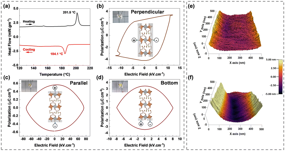 | ||
| Fig. 2 (a) Differential scanning calorimetric measurement. (b)–(d) P–E hysteresis loop studies carried out in perpendicular, parallel and bottom configurations for CPAS single crystals. Insets represent crystal arrangements and optical images of the device. (e) AFM topography image and (f) PFM image of the CPAS single crystal at an applied tip voltage of 5 V. The colour scale is given on the far right. | ||
To further understand the non-centrosymmetric and polarization behaviour of CPAS, polarization–electric field (P–E) hysteresis loop and piezoresponse force microscopic (PFM) studies were carried out. Polarization is expected due to dipole alignment in organic cations and to a lesser extent, in the octahedral sheets due to inter- and intra-octahedral distortion.12P–E loop measurements were carried out in single crystals by taking contacts in different directions: perpendicular, parallel, and bottom. Fig. 2(b–d) depict the crystal structures and connections used.
The device with contacts perpendicular to the octahedral layers shows a hysteresis loop reminiscent of a ferroelectric character with spontaneous (Ps) and remanant polarization (Pr) values of about 3.40 and 2.65 μC cm−2, respectively (Fig. 2(b)). However, when the connections are made in the parallel and bottom configurations (Fig. 2(c and d)), the P–E loop displays an ellipse-shaped curve, indicative of capacitive behaviour. Current–voltage curves associated with P–E loops are provided in Fig. S6 (ESI†).13 Perpendicular contacts exhibit a sharp increase in current attributed to a polarization current, while parallel and bottom contacts demonstrate a conventional DC conduction current. These results imply that the ferroelectricity arises predominantly from the alignment of dipoles in the halogenated organic cations in CPAS. A comparison of polarization and other related properties of different halide ferroelectric materials is provided in Table S3 (ESI†).
Piezoelectric characteristics of CPAS were analyzed using piezoresponse force microscopy (PFM). The atomic force microscopic (AFM) image of the CPAS single crystal was nearly flat (Fig. 2(e)). However, when a 5 V potential was applied to the tip, morphological changes occurred, with some areas contracting and others expanding (Fig. 2(f)). Application of this voltage caused the crystals to distort by about ±5 nm. Three-dimensional (3D) and layout images at different tip voltages are provided in Fig. S7 (ESI†). This piezoelectric study reveals that CPAS responds to the applied mechanical strain. When voltage is applied to the materials with a non-centrosymmetric property, the crystal structure deforms, causing expansion or contraction.14 The difference in the direction of alignment of the dipoles in the material leads either to expansion or to contraction. The P–E loop measurements and PFM imaging further confirm that CPAS is a non-centrosymmetric material. The structural orientation in a 2D layered halide perovskites results in distinct in-plane and out-of-plane properties.
To correlate the role of polarization with the conductivity of the material, impedance measurements were performed on the CPAS single crystals along three different crystal configurations similar to the P–E loop measurements (Fig. 3(a)). The equivalent circuit used for fitting is provided in the inset to Fig. 3(a). The resistance was measured to be 1.45 MΩ cm along the perpendicular contacts, and it decreased to 0.57 MΩ cm for the parallel contacts. The bottom contacts, featuring only an inorganic octahedral sheet connection, exhibited the highest resistance of 5.13 MΩ cm. It has been reported that the organic cations act as an insulating barrier to charge transport, whereas the inorganic octahedral sheets help in the conduction of ions through the layers.15 However, in the present case, we have noticed lower resistance for conduction between layers and high resistance in-plane. This might be attributed to polarized domains, which can localize and confine charge carriers.16
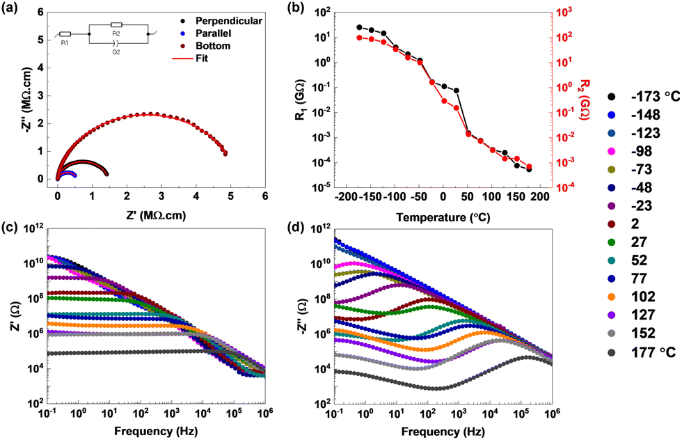 | ||
| Fig. 3 (a) Impedance measurements (Nyquist plots) performed in three different crystal configurations. (b)–(d) Temperature-dependent impedance measurements. (b) Resistance values as a function of temperature. The corresponding Nyquist plots are shown in Fig. S8 (ESI†). (c) and (d) Real and imaginary parts of the impedance as a function of frequency. The temperature scale in °C is given on the far right. | ||
Temperature-dependent impedance measurements were carried out to understand the mechanism of charge conduction in a CPAS pellet (Fig. 3(b–d) and Fig. S8, ESI†). The curves are fitted using a two resistor‖capacitor in series, and the circuit is shown in Fig. S8(a) (ESI†). Fitted R1 and R2 values are provided in Table S4 (ESI†). The value of R1 is approximately 25 GΩ at −173 °C; however, upon increasing the temperature, the resistance drops by over three orders of magnitude, and it reduces to a few hundreds of kΩ above room temperature. The value of R2 also shows a similar trend, but the resistance values are around four times higher than those of R1, with 97 GΩ at −173 °C. The values of R1 and R2 merge at temperatures above 50 °C. R1 and R2 can be attributed to bulk and grain boundary resistances, where at high temperature, grain boundaries gain sufficient energy to enable charge conduction such as the bulk of the material. The decrease in resistance or increase in conductivity with temperature hints at defect- or phonon-mediated conduction in CPAS. To understand the mechanism, the trend in the real (Z′) and imaginary (−Z′′) parts of impedance as a function of frequency was evaluated. Fig. 3(c) shows that the value of Z′ decreases with temperature and frequency, with eventual overlap of the curves at high frequency, indicating the release of space charges. The latter could be attributed to the possible reduction of the barrier for charge conduction. At low frequencies, the decrease in Z′ with temperature shows a negative temperature coefficient of resistance, indicating the semiconducting nature of the material. The imaginary part of impedance shows a steady decrease in −Z′′ as a function of frequency at low temperature; however, at temperatures >−98 °C, a peak starts to appear. The presence of the peak indicates space charge polarization, typical for materials with grains and grain boundaries. The peak maximum starts to shift to higher frequencies with temperature, simultaneously showing a decrease in resistance values. This trend highlights the relaxation of space charge carriers and decrease in the relaxation time at higher temperature. Similar to Z′, the trend in −Z′′ also indicates a reduction in resistance due to a reduction in barrier height enabled by defects or phonons at high temperature. At temperatures beyond 27 °C, a new peak starts to appear at low frequencies. This highlights the presence of a second relaxation mechanism at higher temperature. The AC conductivity (Fig. S9, ESI†) shows one frequency-dependent signature at low temperature, whereas at high temperature two distinct frequency-dependent regions appear. Impedance results confirm temperature-activated conduction possibly due to defect/phonon mediation and show multiple relaxation pathways for charge conduction. This might have contributions from non-polar regions from the bulk of the material, grain boundaries and the polar domain within the bulk.
Following the understanding of conduction properties, optical properties were investigated (Fig. S10, ESI†). The absorption spectrum shows the onset at ∼490 nm, with a bandgap of 2.48 eV (Fig. S11, ESI†). Photoluminescence (PL) emission is found in the range of 400 to 550 nm. Two different PL peaks were observed: a low-intensity high-energy peak centered at ∼425 nm and high-intensity low-energy peak centered at ∼475 nm.17 These peaks are attributed to free/bound excitons and self-trapped excitons, respectively. The photoluminescence emission spectra of CPAS powder samples at different excitation wavelengths with normalized spectra are provided in Fig. S12 (ESI†). The normalized spectra overlap with no new peaks rules out the possibility of non-photoluminescence signatures. To understand the nature of the bandgap, PL excitation measurements were done, where the range of wavelength of illuminated photons responsible for PL emission was studied. The emission monochromator was locked to a given fluorescing wavelength (λem: 500 nm), and the excitation monochromator was scanned within the absorption range of the material below λem. If the absorption and excitation onsets overlap, then this essentially represents a direct bandgap. However, if the excitation onset shows up at a lower wavelength compared to absorption onset, then it can be attributed to an indirect bandgap. CPAS showed an onset of excitation at 425 nm, which is lower than the absorption onset. This result suggests that the CPAS material is an indirect band gap material.18 Based on the composition of orbitals formed in Cs2AgSbBr6 reported in the literature, we believe that in CPAS, the conduction band minimum is a mixture of Sb-5p/Br-4p antibonding orbitals. The valence band maximum is assigned to the bonding orbitals Sb-5s, Ag-4d and Br-4p.19 The photoluminescence quantum yield (PLQY) and CIE (Commission Internationale de l'éclairage) colour coordinates data (0.177,0.131) are provided in Fig. S13, S14 and Table S5 (ESI†). PLQY was found to be 0.5, and the CIE plot indicates blue emission in CPAS. The excited-state lifetime is described in Fig. S15 (ESI†).
In this work, we report a new two-dimensional halide double perovskite ferroelectric material synthesized using a halogenated A-site linker. Although the linker used was purely chloride-based, during synthesis, bromide was partially substituted providing the organic site with mixed halogens. This has possibly led to break in the inversion symmetry to form a non-centrosymmetric compound. The two-dimensional material exhibited directional-dependent properties, where ferroelectric behaviour was noted only in the direction perpendicular to the octahedral sheets. The P–E loop measurements between the sheets or within a sheet yielded a capacitive loop. The conductivity is lower for perpendicular contacts compared to parallel contacts, possibly due to the polar nature of the material. Anisotropic properties make this material exciting for optoelectronic applications that benefit from inbuilt ferroelectric polarization.
Data availability
Crystallographic data for the compound reported in the manuscript has been deposited at the CCDC under 2339849† and can be obtained from https://www.ccdc.cam.ac.uk/.Conflicts of interest
There are no conflicts to declare.Notes and references
- W. Zhang, M. Hong and J. Luo, Angew. Chem., 2020, 132, 9391–9394 CrossRef.
- K. Meng, W. Li, X. G. Tang, Q. X. Liu and Y. P. Jiang, ACS Appl. Electron. Mater., 2022, 4, 2109–2145 CrossRef CAS.
- L. Mao, S. M. L. Teicher, C. C. Stoumpos, R. M. Kennard, R. A. Decrescent, G. Wu, J. A. Schuller, M. L. Chabinyc, A. K. Cheetham and R. Seshadri, J. Am. Chem. Soc., 2019, 141, 19099–19109 CrossRef CAS PubMed.
- P. Guo, C. C. Stoumpos, L. Mao, S. Sadasivam, J. B. Ketterson, P. Darancet, M. G. Kanatzidis and R. D. Schaller, Nat. Commun., 2018, 9, 2019 CrossRef PubMed.
- P. Siwach, P. Sikarwar, J. S. Halpati and A. K. Chandiran, J. Mater. Chem. A, 2022, 10, 8719–8738 RSC.
- C. F. Wang, H. Li, Q. Ji, C. Ma, L. Liu, H. Y. Ye, B. Cao, G. Yuan, H. F. Lu, D. W. Fu, M. G. Ju, J. Wang, K. Zhao and Y. Zhang, Adv. Funct. Mater., 2022, 32, 2205918 CrossRef CAS.
- B. Wang, X. Yang, R. Li, S. M. H. Qaid, W. Cai, H. Xiao and Z. Zang, ACS Energy Lett., 2023, 8, 4406–4413 CrossRef CAS.
- W. Travis, E. N. K. Glover, H. Bronstein, D. O. Scanlon and R. G. Palgrave, Chem. Sci., 2016, 7, 4548–4556 RSC.
- M. V. Kovalenko, L. Protesescu and M. I. Bodnarchuk, Science, 2017, 358, 745–750 CrossRef CAS PubMed.
- P. Siwach, P. Sikarwar, S. A. Rajput, S. Antharjanam and A. K. Chandiran, Chem. Commun., 2022, 58, 10504–10507 RSC.
- B. Dhanabalan, Y. C. Leng, G. Biffi, M. L. Lin, P. H. Tan, I. Infante, L. Manna, M. P. Arciniegas and R. Krahne, ACS Nano, 2020, 14, 4689–4697 CrossRef CAS PubMed.
- P. Siwach, P. Sikarwar, J. S. Halpati and A. K. Chandiran, J. Mater. Chem. A, 2022, 8719–8738 RSC.
- B. Xun, A. Song, J. Yu, Y. Yin, J. F. Li and B. P. Zhang, ACS Appl. Mater. Interfaces, 2021, 13, 4192–4202 CrossRef CAS PubMed.
- T. Y. Kim, S. K. Kim and S. W. Kim, Nano Convergence, 2018, 5, 30 CrossRef PubMed.
- J. V. Passarelli, D. J. Fairfield, N. A. Sather, M. P. Hendricks, H. Sai, C. L. Stern and S. I. Stupp, J. Am. Chem. Soc., 2018, 140, 7313–7323 CrossRef CAS PubMed.
- J. Leveillee, G. Volonakis and F. Giustino, J. Phys. Chem. Lett., 2021, 12, 4474–4482 CrossRef CAS PubMed.
- L. A. Muscarella and E. M. Hutter, ACS Energy Lett., 2022, 7, 2128–2135 CrossRef CAS PubMed.
- T. Appadurai, R. Kashikar, P. Sikarwar, S. Antharjanam, B. R. K. Nanda and A. K. Chandiran, Commun. Mater., 2021, 2, 68 CrossRef CAS.
- Z. Li, S. R. Kavanagh, M. Napari, R. G. Palgrave, M. Abdi-Jalebi, Z. Andaji-Garmaroudi, D. W. Davies, M. Laitinen, J. Julin, M. A. Isaacs, R. H. Friend, D. O. Scanlon, A. Walsh and R. L. Z. Hoye, J. Mater. Chem. A, 2020, 8, 21780–21788 RSC.
Footnote |
| † Electronic supplementary information (ESI) available: Material characterization data and experimental section. CCDC 2339849. For ESI and crystallographic data in CIF or other electronic format see DOI: https://doi.org/10.1039/d4cc01520g |
| This journal is © The Royal Society of Chemistry 2024 |