
Surface acoustic wave induced phenomena in two-dimensional materials
Xuchen
Nie
 *a,
Xiaoyue
Wu
a,
Yang
Wang
a,
Siyuan
Ban
a,
Zhihao
Lei
b,
Jiabao
Yi
b,
Ying
Liu
*c and
Yanpeng
Liu
*a
*a,
Xiaoyue
Wu
a,
Yang
Wang
a,
Siyuan
Ban
a,
Zhihao
Lei
b,
Jiabao
Yi
b,
Ying
Liu
*c and
Yanpeng
Liu
*a
aKey Laboratory for Intelligent Nano Materials and Devices of Ministry of Education, State Key Laboratory of Mechanics and Control of Mechanical Structures, and Institute for Frontier Science, Nanjing University of Aeronautics and Astronautics, Nanjing, 210016, China. E-mail: xcnie@nuaa.edu.cn; chmliuyp@nuaa.edu.cn
bGlobal Innovative Centre for Advanced Nanomaterials, College of Engineering, Science and Environment, The University of Newcastle, NSW 2308, Australia
cCollege of Jincheng, Nanjing University of Aeronautics and Astronautics, Nanjing 211156, China. E-mail: lily_ying2012@163.com
First published on 12th November 2022
Abstract
Surface acoustic wave (SAW)–matter interaction provides a fascinating key for inducing and manipulating novel phenomena and functionalities in two-dimensional (2D) materials. The dynamic strain field and piezo-electric field associated with propagating SAWs determine the coherent manipulation and transduction between 2D excitons and phonons. Over the past decade, many intriguing acoustic-induced effects, including the acousto-electric effect, acousto-galvanic effect, acoustic Stark effect, acoustic Hall effect and acoustic exciton transport, have been reported experimentally. However, many more phenomena, such as the valley acousto-electric effect, valley acousto-electric Hall effect and acoustic spin Hall effect, were only theoretically proposed, the experimental verification of which are yet to be achieved. In this minireview, we attempt to overview the recent breakthrough of SAW-induced phenomena covering acoustic charge transport, acoustic exciton transport and modulation, and coherent acoustic phonons. Perspectives on the opportunities of the proposed SAW-induced phenomena, as well as open experimental challenges, are also discussed, attempting to offer some guidelines for experimentalists and theorists to explore the desired exotic properties and boost practical applications of 2D materials.
I. Introduction
Surface acoustic waves (SAWs) that propagate within the unbounded solid surface with negligible dissipation over macroscopic distances exhibit great potential for regulating electronic and opto-electronic devices.1,2 As low-frequency acoustic phonons, SAWs confine the phonon energy in terms of one to two wavelengths perpendicular to the basal plane. As quasi-two-dimensional (2D) waves in solids, the transmission mode of SAWs is relatively simple, easy to distinguish, and has a low loss. Therefore, SAWs emerge as a fantastic means for exciting solid-state materials in coordination with electrons and photons or magnetic and spin excitations.3,4 To date, by employing acousto-electric, acousto-optic and magneto-elastic coupling effects, phononic circuits and resonators have been widely adopted to guide, circulate and modulate SAWs for sensing5–8 and communications,9,10 especially in life sciences and acoustic microfluidics for sensing and mixing tiny amounts of liquids.11–13 Fundamentally, the propagation velocity (νSAW) of SAWs in solids usually reaches a few thousand meters per second and SAWs with the same frequency with electro-magnetic waves possess five orders of magnitude shorter wavelength, showing great potential in device miniaturizations.14 Benefitting from the strong coupling with elementary excitations in condensed matter, SAWs are ideally suited to probe and control elementary excitations at single quanta limits,15–22 such as superconducting circuits, semiconductor quantum dots and defect centers. Even with respect to collective excitations, classical or quantum phenomena are nowadays coherently interfaced by SAWs. The present SAW–matter interaction studies permeate the interdisciplinary fields of materials sciences, photonics, biomedical, and quantum science, giving rise to tremendous phenomena,14 such as phononic quantum communications,23–28 acousto-optic modulations,29–31 electro-acoustic modulations,32 and spin–phonon interactions.33–362D materials, owing to their atomic thickness and extremely large surface-to-volume ratio, allow external stimuli (electric fields and SAWs) to modulate their inherent optical, electrical, and opto-electronic properties.37–44 In 2D limit, dielectric screening is reduced while Coulomb interactions and excitonic emissions (exciton, trion and biexciton) are extremely enhanced.45 However, the atomic thickness of 2D materials signifies indispensable supporting substrates for most fundamental research and applications. Therefore, the coupling between 2D materials and underlying substrates has blossomed into one promising key for controlling 2D material properties. In this regard, by placing 2D materials onto piezo-electric substrates, the as-generated SAWs under electrical excitations as well as the corresponding dynamic strains and piezo-electric fields concentrated at substrate surfaces were proven to modulate the lattices and electronic structures of 2D materials in an elegant manner. Moreover, for certain 2D materials with trigonal prismatic structures, such as MoS2 and WS2 monolayers, SAWs could break the inversion symmetry and give impetus to fantastic piezo-electricity and strain modulations.46–48
Herein, we review the research progress of SAW-induced emergent phenomena (as shown in Fig. 1) in 2D materials, such as semi-metallic graphene and semiconducting transition metal dichalcogenides (TMDCs), mainly excited by interdigital transducers (IDTs) on piezo-electric substrates. This minireview is organized as follows: first, we brief the basic coupling feature between SAWs and 2D materials; then, we classify our discussions into Type-I and Type-II band edge modulations by dynamic strains and piezo-electric fields associated with SAW propagation. The confronted challenges and feasible future directions are also provided. We hope this timing review will offer intuitive understanding of the SAW-induced emergent phenomena in 2D materials and also provide possible opportunities for both new comers and experiential experts.
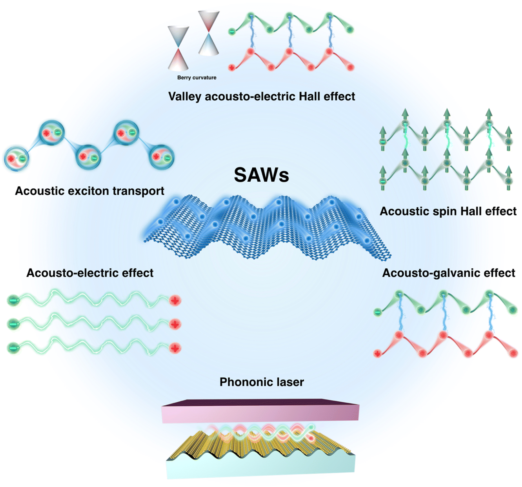 | ||
| Fig. 1 Schematic representation of intriguing acoustic-induced phenomena, including the acousto-electric effect, acousto-galvanic effect, acoustic exciton transport, valley acousto-electric Hall effect, acoustic spin Hall effect, and phononic laser. | ||
II. Surface acoustic waves
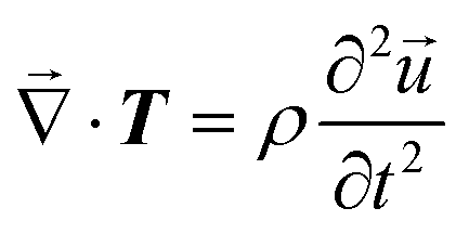
In general, SAWs can be classified into Rayleigh, shear-horizontal, Lamb and Love waves.49 Among the diverse modes of SAWs, Rayleigh waves, in which the modal superposition of longitudinal and shear vertical wave components occurs under traction-free boundary conditions on piezo-electric substrates, have attracted the most research attention owing to their applicability in a vast variety of transducers.2 In Rayleigh waves, the surface particles move in an elliptical fashion that is normal to the surface and parallel to the direction of acoustic propagation.1 The polarization plane of Rayleigh waves is perpendicular to the substrates and the amplitude of the particle motion decays exponentially with a penetrating depth (an effective penetration depth usually less than one wavelength). It is found that the velocity of Rayleigh waves is determined using the Poisson's ratio and shear wave velocity, and thus, the substrate material and its corresponding crystal orientation are the essential parameters that should be taken into account in the first place.2To obtain desirable SAWs, electrical excitations based on the inverse piezo-electric effect50–54 and optical excitation in light of elastic stresses upon laser radiation55–57 are two prevalent methods. For the former one, SAWs are mainly generated, detected, and controlled by employing IDTs. IDTs are periodic arrays of metallic finger electrodes with a pitch of half the SAW wavelength (λSAW). Two interlocking electrodes are deposited on piezo-electric substrates and connected to a frequency generator.58 Piezo-electric crystals with dipoles re-oriented along certain directions under external electric fields, such as quartz, lithium niobate (LiNbO3) and lithium tantalate (LiTaO3), generate directional propagations of mechanical deformation waves along piezo-electric surfaces. As shown in the inset in Fig. 2, acoustic actuation is launched by applying a high frequency input signal between transmitting IDTs to achieve SAWs with a targeted frequency (f = νSAW/λSAW, where νSAW and λSAW represent the velocity and wavelength of SAWs), complying with the inverse piezo-electric effect. Because of the mechano-electrical coupling of piezo-electric substrates, the IDTs at the receiving end produce electrical signals, referred to as acoustic sensing. By designing the spacing and geometry of electrodes, appropriate SAWs could be selectively emitted toward distinct applications.58–60 In particular, the dispersive delay line (chirped) configuration with varying spacings could produce altered frequencies between electrodes that range from 20 MHz to 125 MHz bandwidths.61 Moreover, the periodic waveforms of high SAW harmonics with arbitrary shapes might also be manifested by changing the unit cell patterns.62 For the majority of electrical SAW excitations, the dominant working principle is based on the inverse piezo-electric effect. In a stress-free planar surface of a semi-infinite isotropic half-space, SAW modes could be expressed by solving the elastic wave equation for the acoustic displacement field ![[u with combining right harpoon above (vector)]](https://www.rsc.org/images/entities/i_char_0075_20d1.gif) (
(![[r with combining right harpoon above (vector)]](https://www.rsc.org/images/entities/i_char_0072_20d1.gif) , t) that decays towards zero as it penetrates into the bulk counterpart63
, t) that decays towards zero as it penetrates into the bulk counterpart63
 | (1) |
![[x with combining circumflex]](https://www.rsc.org/images/entities/i_char_0078_0302.gif) -axis, the solutions of the elastic equation must also satisfy the constitutive relationships
-axis, the solutions of the elastic equation must also satisfy the constitutive relationshipsT = cS − d![[E with combining right harpoon above (vector)]](https://www.rsc.org/images/entities/i_char_0045_20d1.gif) |
![[D with combining right harpoon above (vector)]](https://www.rsc.org/images/entities/i_char_0044_20d1.gif) = dS + ε = dS + ε | (2) |
| Tiz(z = 0) = 0, (i = x,y,z) |
| Dz(z = 0+) = Dz(z = 0−) | (3) |
is the electric displacement field and 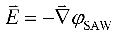 is the piezo-electric field (expressed in terms of the piezo-electric potential φSaw). To our limited knowledge, the drawback of electrical excitation methods is the complexity of matching large SAW amplitudes with small quantum objects. Moreover, broadband SAWs are strictly prohibited in IDTs and the current piezo-electric materials are unsatisfying. The key properties of appropriate piezo-electric materials include the electro-mechanical coupling factor (k2) that determines the piezo-electric coupling efficiency, the coefficient of thermal expansion, the acoustic velocity (νSAW), compatibility, and finally the expense of raw materials.2Table 1 summarizes the popular piezo-electric materials and their corresponding parameters. For certain bulk piezo-electric materials, orientational cutting may generate particular types of SAWs and affect the acoustic velocity. For example, 128° and 41° YX cutting of LiNbO3 were found to generate Rayleigh and shear-horizontal waves, respectively. The acoustic velocity of the LiNbO3 crystal was increased to 3992 m s−1 (128° YX cutting one) from 3488 m s−1 (pristine, no orientational cut).2 Thin-film piezo-electric materials, including aluminum nitride (AlN), zinc oxide (ZnO), and piezo-ceramics, have also attracted broad attention in lab-on-chip and acousto-fluidics devices due to their flexibility and selective deposition compatibility.64–67 Among them, AlN films were reported to exhibit the highest acoustic velocity (5800 m s−1) and high temperature resistance,65 while piezo-ceramics exhibit the largest piezo-electric constant (d33 = 110 pC/N for PZT, lead zirconate titanate) and electro-mechanical coupling.67
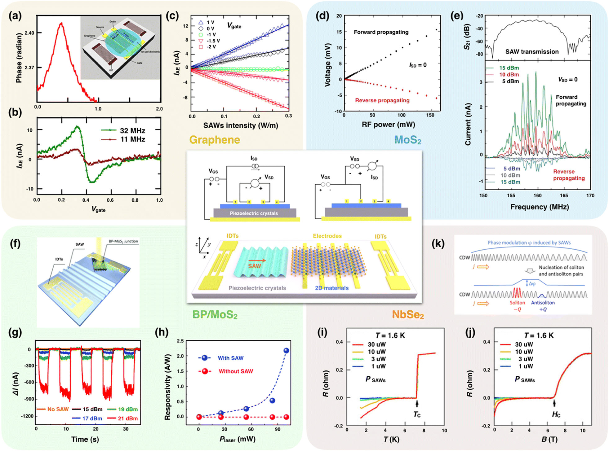 | ||
| Fig. 2 Acousto-electric effect. (center) Device schematics of SAW excitation and detection with a basic delay line electrode configuration consisting of two IDTs on piezo-electric substrates. The left IDT generates a surface Rayleigh wave propagating along the axis that is read out by right IDTs. The insets show the electrical wiring configurations for 4-point (left) and 2-point (right) measurements of the acoustic charge transport. (a and b) Measured SAW phase and AE current vs. gate voltages (Vgate) in graphene/LiNbO3 devices. Inset: Schematic diagram of the device. (c) AE current as a function of the SAW intensity (at 32 MHz) for three different Vgate. Reproduced from ref. 97 with permission from Tsinghua University Press, copyright 2016 (Open access). (d) AE voltage vs. radio frequency (RF) power plots of the hybrid monolayer MoS2/LiNbO3 device via a 4-point open-circuit (ISD = 0) configuration. For forward and backward SAW propagation directions, the expected linear dependences are well reproduced. The signs of AE currents and voltages correspond to the n-type conductivity of the film. (e) SAW transmissions and propagations. The frequency band of SAW transmission between IDTs plotted as the scattering parameter S21 (top panel). The AE current as a function of the applied radio frequency for different RF power levels in a 2-point short-circuit (VSD = 0) configuration (bottom panel). Reproduced from ref. 98 with permission from Springer Nature, copyright 2015 (Open access). (f) Schematic layout of the IDTs and BP/MoS2 p–n heterojunction. (g) Photocurrent (Iph) variations at different RF powers under a light illumination of 100 mW. As the applied RF power increases to 21 dBm, Iph increases sharply to 900 nA, overwhelming the value in the absence of SAWs (∼280 pA). (h) Photo-responsivity comparison with and without SAW excitations at different laser powers. Reproduced from ref. 99 with permission from Royal Society of Chemistry, copyright 2018. (i and j) Temperature and magnetic-field dependent resistances of the NbSe2 device under different excitation powers at 1.6 K. (k) Schematics showing the nucleation of soliton and antisoliton pairs. One possible scenario for reproducing the negative resistance is irradiating SAWs to generate soliton–antisoliton pairs in the CDW phase, which forms local capacitances in the superconducting domains. When SAWs irradiate the CDW states of NbSe2 (below 33 K), all selenium atoms would be shifted from the commensurate position, and thus, the CDW phase φ is modulated over the SAW wavelength (top panel). This displacement increases the electrostatic energy and elastic energy. Thus, in the superconducting state (below Tc = 7.2 K), it is energetically more favorable to nucleate soliton–antisoliton pairs and induce a 2π phase difference between the soliton and antisoliton pairs (bottom panel). Reproduced from ref. 100 with permission from American Association for the Advancement of Science, copyright 2020. | ||
| Piezo-electric materials | Orientation/cut | Piezo-electric coefficient (d33, pC/N) | Acoustic velocity (m s−1) | Density (g cm−3) | Thermal expansion coefficient (×10−6/°C) | Elastic modulus (GPa) | Electro-mechanical coupling coefficient (k2, %) |
|---|---|---|---|---|---|---|---|
| Quartz | X axis | 2.3 (d11) | 3159 | 2.65 | — | 97.2 | 0.14 |
| Quartz | ST-cut | 2.3 (d11) | 3159 | 2.65 | — | 71.7 | 0.03 |
| LiNbO3 | YZ-cut | 6 | 3488 | 4.65 | — | 202 (C11) | 0.045 |
| LiNbO3 | 128°YX -cut | 12 | 3992 | 4.65 | — | 202 (C11) | 5.3 |
| LiTaO3 | YZ-cut | 8 | 3230 | 7.46 | — | 233 (C11) | 0.66 |
| LiTaO3 | X-cut | 5.7 | 3290 | 7.46 | — | 233 (C11) | 0.75 |
| BaTiO3 | — | 160 | 4392 | 5.70 | — | 110 | 0.34 |
| PZT | — | 110 | 3900 | 7.50 | — | 60 | 20–35 |
| ZnO | — | 12 | 2720 | 5.61 | 6.50 | 140 | 1.5 |
| GaAs | — | 3.4 | 4730 | 5.32 | 5.73 | 86 | 0.07 |
| GaN | — | 4.5 | 4130 | 6.15 | 3.17 | 320 | 0.13 |
| AlN | — | 4.5, 6.4 | 5800 | 3.30 | 5.20 | 300–350 | 3.1–8 |
With reference to electrical excitations, the optical excitations are reported to be capable to obtain SAWs with spectral widths up to several GHz (known as acoustic phonons).55,68 In pump–probe configurations, typically, the picosecond/femtosecond laser is split into pump and probe pulses, where the pump pulse generates ultrafast ultrasonic waves into target samples via photo-thermal and thermo-mechanical couplings, and then the probe pulse reflected from the sample surface is used to measure the pump-induced ultrasonic waves in the GHz to THz range by interferometric and reflectometric methods.69,70 For the interferometric method, the Michelson, Mach–Zehnder, and Sagnac interferometric techniques are preferred to measure the absolute optical phase of the reflected probe pulse that is sensitive to the surface displacements.71–74 Therefore, outstanding sensitivity and spatial resolution to very tiny acoustic vibrations in the ultra- and super-high-frequency ranges could be expected.74,75 However, the implementation of interferometry in the picosecond/femtosecond time scale demands precise stabilization systems, and the phase calibration becomes complicated. In contrast, the reflectometric method measures the small intensity variation of probe reflection due to the photo-elastic coupling of material reflectivity with ultrasonic waves. For ensuring the simplicity in implementations, lock-in amplifying by using knife-edge76 and beam distortion detection77 techniques that precisely capture the surface displacements are the mainstreams. By introducing local heating and thermo-elastic expansion on 2D surfaces via focused ultra-short laser pulses, broadband SAW pulses might be excited within any absorbing material in the ultrasound region in theory. The mere limitation of the SAW amplitude relies on the damage threshold of 2D materials. In a nutshell, the optical excitation method paves the way for systematically investigating the linear and nonlinear elastic properties of 2D materials and their heterostructures in the frame of thermo-elastic and ablative or explosive evaporation mechanisms, respectively.
III. SAW-induced emergent phenomena in 2D materials
Since the mechanical exfoliation of graphene in 2004, 2D materials have been increasingly explored in the multidiscipline research community of condensed matter physics, electronic engineering, materials science, and chemistry.78 Graphene attracts enormous interest due to its fascinating optical transparency and ultrahigh carrier mobility, but the absence of an electronic bandgap (a zero-overlap semimetal) moves one of the research focuses to 2D semiconductors. For instance, the TMDC monolayer with the formula MX2 (where M is a transition metal and X is a chalcogen) possess M atoms sandwiched between two X layers and lack the inversion symmetry.46–48 In addition, the family of TMDCs consists but not limited to the semiconducting (M = Ti, Hf, Zr, Mo, and W) and metallic or semi-metallic (M = V, Nb, and Ta) materials. The broken inversion symmetry of the TMDC monolayer (such as MoS2 and WS2) gives rise to the piezo-electricity and its modulations by external stimuli. Because of significant quantum confinement effects and reduced dielectric screening, the optical properties of TMDCs are dominated by excitonic effects that may be influenced by external fields.79 In addition, the valley/spin degree of freedom and strong spin–orbit coupling enable TMDCs full of emergent phenomena that may be excited or controlled by various regulatory means. The outstanding specific surface areas of 2D materials offer many rooms for interfacial coupling, enabling 2D materials ideal candidates for SAW devices.80 The strain fields of SAWs dynamically modulate the optical and vibrational properties of graphene and other 2D materials and become an exciting test-bed for many emerging phenomena and particle transport in media toward electronic and opto-electronic devices for information processing and communication.4 In addition, the piezo-electric fields associated with SAWs probably interact with charge carriers within 2D materials. Hence, the interaction between propagating SAWs and 2D materials attracts intense attention. Over the past decade, many intriguing acoustic-induced effects, including the acousto-electric effect,81–86 acousto-galvanic effect,86–88 acoustic Stark effect,89,90 acoustic Hall effect and acoustic exciton transport,91,92 have been experimentally reported by manipulating 2D materials with SAWs. In the meantime, the valley spin-acoustic resonance,93 valley acousto-electric effect94,95 and acoustic spin Hall effect96 were theoretically proposed, awaiting for further experimental verifications.A. Acoustic charge transport
 | (4) |
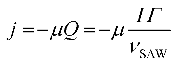
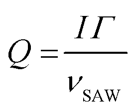 is the phonon pressure, I is the SAW intensity, and Γ is the attenuation coefficient given by82,83
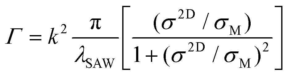 | (5) |
This is a non-monotonic function of the diagonal component of a conductivity tensor σ2D and reaches a maximum at the characteristic conductivity σM. During last few years, the AE effect in 2D materials has been extensively investigated toward applications as metrology and quantum information processing.104 For instance, the SAW excitations of graphene generated a direct AE current in graphene/piezo-electric substrates.63 The AE current (Fig. 2a–c) was found to increase linearly with SAW frequencies and powers82,83 and could be reversed and switched off by a gate voltage.97 The flow of induced currents and the accumulation of longitudinal voltages in graphene were further verified under different experimental conditions, including varying temperatures, carrier concentrations, piezo-electric substrates and wiring schemes.81–86 The coupling of piezo-electric fields with electron gas modifies the propagation velocity, and even amplify the SAW intensity within a graphene plane.97,105–107 Through illuminating a hybrid graphene/LiNbO3 structure, Tynyshtykbaev et al. pioneerly reported the SAW-induced photo-acoustoelectric amplification in 2021. The appearance of an additional current and reduced collisional scattering of photo-induced electrons under the piezo-electric field proved the origin of the SAW-induced photo-acoustoelectric effect.107 In addition, the periodic electric and strain fields of SAWs were also adopted to manifest the graphene Dirac cone108 and even couple lights into plasmons.109
In afore-mentioned studies, the majority of 2D materials interplaying with SAWs were mechanically exfoliated from mother crystals and the lateral size was usually limited to below few tens of millimeters. In addition, several unavoidable transfer processes might have introduced wrinkles and tear 2D materials into smaller pieces, adding to difficulty in massive productions. In this concern, epitaxial growth of 2D materials onto SAW substrates (quartz and LiNbO3) was attempted. Preciado et al.98 successfully developed a millimeter-scale MoS2/LiNbO3 structure by chemical vapor deposition (CVD) methods, followed by lithographically defining a field-effect transistor (FET) structure on the top. The acousto-electric activity of the LiNbO3 substrate permits concomitant probing and manipulating the electronic and optical properties of 2D materials in a contact-free manner. Fig. 2d and e show the strong acousto-electric effect and enhanced photo-conductance of the epitaxial monolayer MoS2 on the LiNbO3 substrate.
Stimulated by the success of single 2D materials, Zheng et al.99 proposed a p–n diode by fabricating a BP/MoS2 van der Waals (vdWs) heterojunction onto SAW platforms. Under the pronounced piezo-electric fields, the p–n heterojunction diode achieved an ultra-high photo-responsivity of 2.17 A W−1 at a wavelength of 582 nm (Fig. 2f–h), nearly 103 times higher than the value achieved without SAWs. Departing from the monolayer MoS2/Au nanoparticles, a Love-mode SAWs aptasensor with dummy fingers was developed and exhibited sensitive and rapid detections of alphafetoprotein in serum in the range of 0.01–100 ng mL−1 with the lowest detection limit of 4.79 pg mL−1.110 The demonstration of sensitive visible-light and protein detection unravels the feasibility of implementing SAWs into next-generation photodiodes and sensors.
Owing to the concurrence of broken inversion symmetry and strong spin–orbit coupling in TMDC monolayers, the electrons (or excitons) at two valleys (K or K′) in the momentum space show opposite spin states with equal energy. Hence, the carriers from extraordinary K (K′) valley states couple exclusively with right (left) circularly polarized light in accordance with the valley-dependent optical selection rule. The coherent control of valley pseudospin by polarized lights provides a nontrivial degree of freedom to manipulate carriers and encode information. Because of the nonzero symmetrical Berry curvature, the in-plane electric field will give impetus to Hall currents with the valley-index dependent sign, defined as the valley Hall effect.37,111 In addition, by placing non-centrosymmetric TMDC monolayers onto piezo-electric substrates, the valley acousto-electric effect and the valley acousto-electric Hall effect were predicted using SAWs. The essence of the valley acousto-electric effect lies in the emergence of a drag electric current (and a spin current) and the contribution of the as-generated current was assigned into three parts: one is the conventional diffusion current that is independent of the valley index and proportional to the acoustic wave vector; the other is the Hall-like warping current due to the trigonal warping of electron dispersion; the third is the acousto-electric valley Hall current caused by the Berry phase acquired by Bloch electrons traveling along the 2D crystal.94,95
In the community of strongly correlated electronic 2D systems, SAWs were attempted to modulate the interplay between charge-density wave (CDW) and superconductivity. In superconducting NbSe2 thin films on the LiNbO3 substrate, Yokoi et al.100 reported the SAW-induced negative resistance (a voltage decrease along the opposite direction of the current flow at zero bias) and found that the amplitude of negative resistance increased by elevating the SAW power and lowering the temperature (Fig. 2i–k). The observation of negative resistance states might become essential in verifying SAW-driven Floquet engineering in superconducting states. In heavy-fermion chiral superconductors, the coupling of SAWs with clapping modes, which are relative amplitude and phase modes between the two chiral components of Cooper pairs, also generates an anomalous transverse electric current in addition to the alternating AE current.85 This anomalous AE effect in chiral superconductors is supposed to be a universal feature and therefore, more research investments may expedite fantastic SAW-induced phenomena.
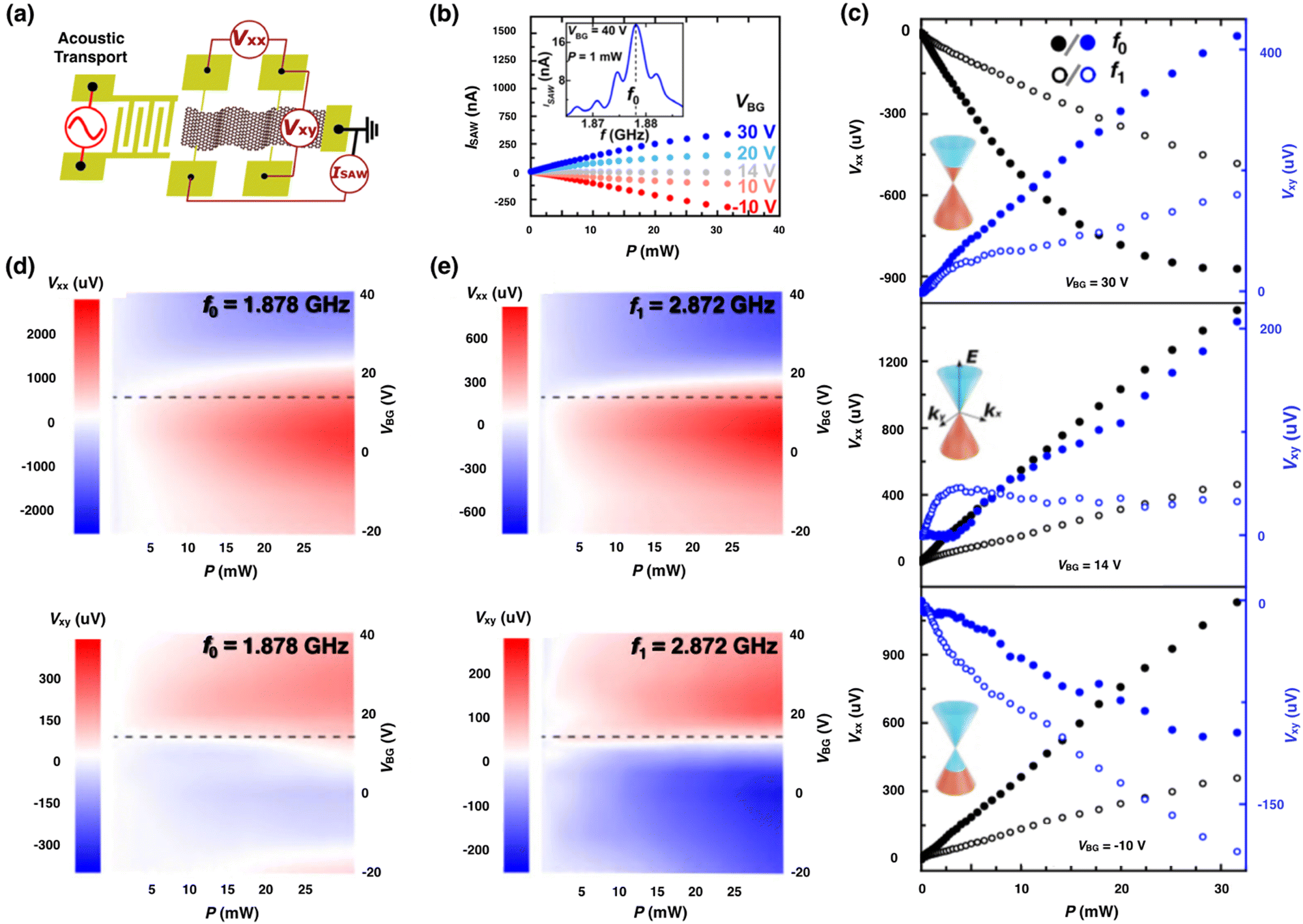 | ||
| Fig. 3 Acousto-galvanic effect. (a) Device configuration of acoustic transport in graphene. A microwave frequency is applied to the IDTs. The monolayer graphene on hybrid piezo-electric substrates was patterned into Hall bar geometry and the acoustic current (ISAW) was measured in the 2-point short-circuit configuration. (b) Plots of ISAW evolution as a function of the IDT frequency, power, and back gate voltage (VBG). (c) Acoustically induced voltages Vxx as a function of the IDT power for the fundamental (f0), first (f1) resonance and three different carrier concentrations at B = 0 T (i.e. the electron regime, the charge neutrality point (CNP), and the hole regime controlled by VBG). The sign of Vxx reflects the dominating carrier type in the graphene layer and is negative (positive) when the Fermi energy resides in the conduction (valence) bands. (d and e) The longitudinal voltage Vxx and transverse voltage component Vxyversus the IDT power, resonances and gate voltages at 4.2 K. The acoustically induced giant synthetic transverse Hall voltage Vxy is positive in the electron regime, approaches zero around the CNP, and then changes the sign once entering the hole regime. The dashed line marks the charge neutral point. Reproduced from ref. 87 with permission from American Physical Society, copyright 2022. | ||
B. Acoustic exciton modulation
The propagating mechanical deformation (dynamic strain field) and the piezo-electric field of SAWs have been successfully employed to transport carriers and spin packets in semiconductor quantum wells (QWs) and modulate the optical emission of single nanostructures. Long-living spatially indirect excitons (IXs, also referred to as interlayer excitons) can be captured by a two-level trap after transport, leading to the emission of single photons.119 For instance, Yuan et al. demonstrated the acoustic manipulation of single exciton centers (individual excitons bound to shallow impurity centers) embedded in GaAs QWs, by a high-frequency (3.5 GHz) and 800 nm-wavelength SAW. In particular, the GHz-SAW field can pump single exciton states bound to impurities that act as two level states to emit anti-bunched photons, enabling the exciton manipulation and exciton-based single-photon sources at microwave frequencies using acoustic waves.120Type-II spatial carrier separation could be induced by the piezo-electric potential along the SAW propagation direction, where the piezo-electric potential ionizes the optically excited excitons and transports the as-generated electrons (holes) within the potential maxima (minima). In this way, the acoustic-induced photoluminescence (PL) quenching arises from exciton ionization (i) followed by the spatial separation of the free electrons and holes (ii) and transport out of the detection area (iii). In addition, the SAWs can increase the radiative recombination lifetime and thus may favor non-radiative recombination channels for PL quenching. The exciton ionization rate depends on the field amplitude and conversely, the travelling piezo-electric field associated with Rayleigh SAW managed the reversible manipulation of excitonic PL in 2–4 layered MoS2 nanoflakes. It is shown that the interplay between photo-generated carriers, excitons, and the SAW piezo-electric field leads to strong dependence of the PL intensity on the SAW amplitude and excitation intensity.121 Subsequently, at moderate SAW powers, researchers from the same group118 observed a strong PL quenching followed by an energy blue-shift of the neutral and negatively charged exciton (trion) emission bands (Fig. 4a–d). The dissociation and spatial separation of excitons were also observed because of the acoustically generated electric field arising from the intrinsic piezo-electricity of odd layers of MoS2 flakes.122 This intrinsic piezo-electricity may be quite promising in improving the electron–hole dissociation efficiency in photovoltaic cells. In 2021, Sheng et al.123 further demonstrated that the exciton characteristics strongly depend on the layer numbers of MoS2 sheets. Under acoustic excitations, the PL quenching in odd MoS2 layers is remarkably larger than that in even layers without piezo-electricity. Moreover, the PL peak position of odd MoS2 layers is blue-shifted with an increment of acoustic powers but remains unchanged in even MoS2 layers.
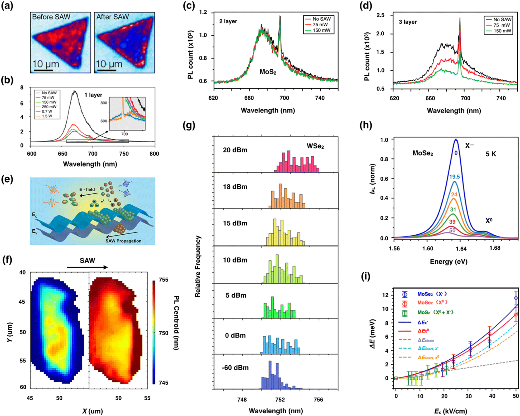 | ||
| Fig. 4 Acoustic exciton modulations. (a) PL mapping of monolayer MoS2 flakes before and after SAWs. The acoustic exciton dissociation and transport in 2D semiconductor materials exposed to SAWs, directly monitored through spatially and time-resolved PL microscopy. (b) PL spectra evolution of monolayer MoS2 flakes by changing SAW input powers. At input powers ≤150 mW, strong quenching can be observed together with an apparent blue-shift of the PL peak due to the ionization of trions into excitons by electric fields, triggered as a consequence of the inherent piezo-electricity by mechanical vibrations using SAWs. At input powers ≥0.25 W, heat generation becomes significant and shifts the PL peak toward higher wavelengths (red-shift). (c and d) PL spectra of bilayer and trilayer MoS2 flakes with and without SAWs. Reproduced from ref. 118 with permission from American Chemical Society, copyright 2016. (e) Illustration showing the conduction and valence band potential fluctuations along the carrier transport path induced by piezo-electric fields. (f) PL centroid map of the WSe2 monolayer at −60 dBm and 20 dBm power levels. (g) Histogram of the PL centroid extracted from the PL mapping (f). Reproduced from ref. 89 with permission from American Chemical Society, copyright 2021. (h) PL spectra of the monolayer MoSe2 for a series of in-plane SAW fields (Ex) ranging from 0 to 50 kV cm−1. (i) The negatively charged trions (X−) and neutral exciton (X0) emissions red-shift ΔE as a function of Ex. The dashed cyan and orange lines are the Stark shift contributions ΔEStark to ΔE extracted from fits. Reproduced from ref. 90 with permission from American Chemical Society, copyright 2021. | ||
Fig. 4e–g show the interaction of excitons in the monolayer WSe2 with the SAW piezo-electric field (type-II bandgap modulation) at room temperature investigated by PL spectroscopy. As can be seen, intense PL quenching is observed with increasing SAW powers because of the dissociation of excitons and trions into free carriers by the in-plane electric field. The PL centroid map and the corresponding histogram clearly show red-shift under SAW excitation, which is attributed to the acoustic Stark effect. By utilizing photo-generated free carriers, the author further demonstrated that the exciton-piezo-electric field interaction and population distribution between neutral excitons and trions could be optically manipulated by the screening field.89 Similarly, Fig. 4h–i show the successfully manipulating excitonic emission energies (i.e. the acoustic Stark effect) and dissociate excitonic states in the monolayer MoSe2 by the in-plane piezo-electric field at 5 K. The high dielectric constant of the LiNbO3 substrate strongly reduces the neutral exciton binding energy, leading to efficiently quench (above 90%) and red-shift of the excitonic emission energies.90 Additionally, the strong coupling between excitons in 2D semiconductors and surface plasmons from 2D materials was predicted to produce SAW-accessible exciton–plasmon polaritons. The strain fields of SAWs create optical diffraction gratings that provide the momentums matched with the surface plasmon, canceling out the piezo-electric field that could dissociate excitons. This is exemplified for the MoS2 monolayer and black phosphorus (BP) mono- and few-layer placed on the top of the thin silver/LiNbO3 substrate.124
Defect centers in 2D materials possess atomic-like optical emission and could couple efficiently with SAWs and related strain and piezo-electric fields in the frequency range of hundreds of MHz. Similar to external RF fields, SAWs can modulate the emission energies and induce resonant transitions between their spin sublevels. Coherent interactions between SAWs and defect centers have been demonstrated for single negatively charged nitrogen-vacancy17,35 and silicon-vacancy34,125 centers in diamond, and neutral di-vacancy centers in silicon carbide (SiC).20 In terms of 2D materials, Iikawa et al.126 investigated the dynamic modulation of optically active defect centers in hexagonal boron nitride (h-BN) layers using SAWs. The dynamic strain field of SAWs modulates the emission lines, resulting in intensity variations as large as 50% and oscillations of the emission energy with an amplitude of ∼1 meV.
C. Acoustic exciton transport
Electrons play an essential role in transmitting information but suffer from the nanosecond response time owing to the strong Coulomb interaction in opto-electronic devices.127 Excitons, electron–hole pairs coupled by the Coulomb interaction, are hydrogen-like bosonic quasi-particles (elementary excitation) with a Bohr radius of nanometer dimension and the main quasi-particles mediating the interaction between light and electronic excitations in semiconductors. Excitons can be optically excited and read out, thereby encoding and storing optical signals into excitons' spin, valley, and orbital degrees of freedom.128,129 Excitonic devices, operating through the generation, diffusion and detection of excitons, hold great promise for overcoming the dilemma of electron and photon-based elements toward realizing efficient interconnects between optical data transmission and electrical processing systems. The potential advantages of excitonic devices include energy-efficient signal processing and seamless coupling with optical communications.The spatial–temporal dynamics of exciton generation, annihilation and spatial diffusion could be separately investigated due to their different time scales. Assuming that none in-plane electric field is applied and the many-body interactions between exciton–trion and exciton–phonon could be ignored, the spatial–temporal dynamics of exciton can be written as127
 | (6) |
 is the position vector (x and y are in-plane coordinates), Δ = ∂2/∂x2 + ∂2/∂y2 is the Laplace operator, τ is the exciton recombination lifetime, Deff is the effective diffusion coefficient of the exciton, and β is the exciton–exciton annihilation rate, respectively. The second and third terms represent the diffusion and Auger recombination, respectively. For exciton diffusion in the low-density regime (i.e. linear diffusion) that the Auger process (∼βN2) was ignored; eqn (6) can be simplified as
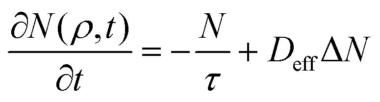 | (7) |
The initial exciton density excited by laser pulses is assumed as N0 and the analytical solution is expressed as 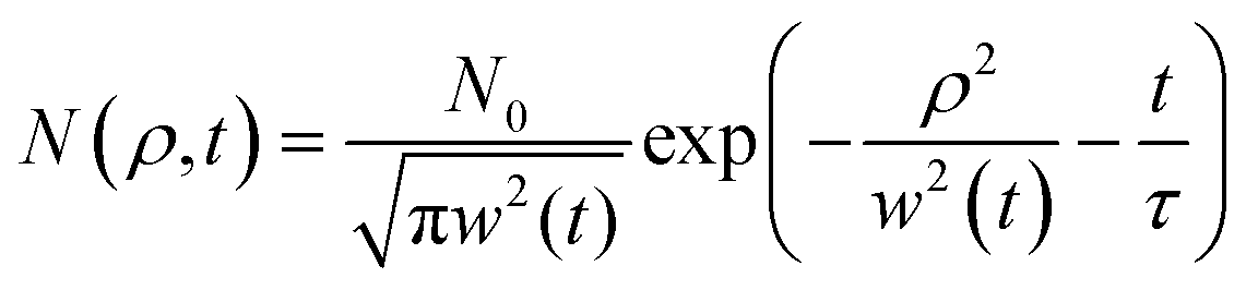 , where
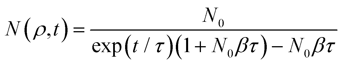
 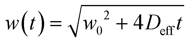 is the spatial distribution width of the exciton density and w0 is the width of excitation beams. In the high-density regime (i.e. nonlinear diffusion), the Auger process is remarkably faster than exciton diffusion. By ignoring the spatial diffusion of excitons, thus eqn (6) can be simplified as
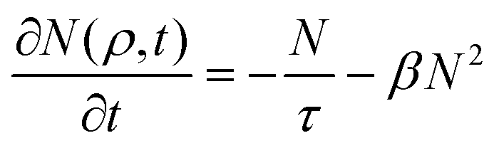 | (8) |
 . By using the solution of eqn (7) as the initial spatial–temporal distribution of excitons, the nonlinear diffusion could be approximately solved with the effective diffusion coefficient Deff = D + βN0w02/16, where D is the intrinsic diffusion coefficient.130 In addition to the exciton–exciton annihilation in the nonlinear diffusion regime, the repulsive exciton interactions that composed the dipolar repulsion and exchange interaction may also significantly improve Deff of the exciton. The exchange interaction decreases with increasing electron–hole separation and becomes negative when the vertical separation is larger than the Bohr radius. For IXs in TMDC heterostructures, the electron–hole separation approximates the Bohr radius of IXs (∼1 nm), thus the exchange interaction is negligible. After taking the repulsive exciton interaction into account, the drift-diffusion equation becomes capable to quantitatively describe the spatial–temporal evolution of the IX density
 | (9) |
For excitonic devices, an outstanding exciton transport distance with a controlled directionality is desired to transmit information over sizable distances. However, a moderate in-plane electric field may dissociate excitons due to its small binding energy, extremely limiting the practical application of excitonic devices. Generally, excitons in quasi-0D systems (molecular and quantum dots) have low diffusion lengths (1–50 nm)151 at room temperature, as the diffusion mainly occurs by site hopping. One-dimensional (1D) single-wall carbon nanotubes have larger exciton diffusion lengths (∼300 nm), depending on the chirality and dielectric environment.144,152,153 In bulk semiconductors, strong dielectric screening generally leads to low exciton binding energy, so excitons exist (maximum diffusion length ∼10–1000 μm) only at cryogenic temperatures,120,131,132 unsatisfying for practical applications.
Owing to the reduced dielectric screenings, enhanced Coulomb interactions, and relatively large effective masses of charge carriers, excitons in 2D TMDC monolayers have a Bohr radius of ∼1 nm and a binding energy of ∼500 meV with strong resonances even at room temperature, making them promising for a plethora of opto-electronic and quantum applications.127 Furthermore, even larger exciton diffusion lengths can be achieved in TMDC-based devices, either by separating electrons and holes in different layers in type-II vdWs heterostructures (where the conduction band minimum and valence band maximum are located in two different layers),154–159 or by using inhomogeneous strain profiles to funnel excitons (i.e. the exciton funneling effect)133–137 that largely reduce exciton–phonon scattering.160,161 The separation between the electron and hole layers allows controlling the overlap of electron and hole wave functions and achieving long IX lifetimes, orders of magnitude longer than lifetimes of spatially direct excitons (DXs, also referenced as intralayer excitons).162 In other words, IXs travel longer distances before recombination. In addition, for MoS2/WS2 and WSe2/WS2 heterostructures with the type-II band alignment, photoexcited DXs turned into IXs on ultrafast timescales of less than 50 fs, promising toward excitonic devices operating at room temperature or even higher temperatures.163,164 Another appealing strategy to control and enhance exciton transport could be generating a time-varying (dynamic) inhomogeneous strain profile by SAWs.134 The spatial modulation of both the conduction and valence bands with opposite phases (type-I bandgap modulation) creates periodic spatiotemporal traps that behave as an efficient conveyor for excitons. The propagating SAWs from the piezo-electric substrate will generate a near-field piezo-electric field with an out-of-plane field (Ez) amplitude up to 107 V m−1 at an acoustic power density of 1 mW μm−1. As such, the Ez component will periodically modulate the IX energy in space and time, creating a dynamic trapping potential for IXs in the extrema of Ez. As the SAWs propagate, the IXs will drift along the time-varying gradient of Ez and thus be carried by the SAWs like surfing on water waves, traveling a longer distance before recombination. In addition, SAWs might also permit us to generate strain along multiple axes and tailor the strain fields. For example, a biaxial strain pattern could be generated by either using orthogonal SAWs or selecting crystal cuts and propagation directions.91
To control the directional transport of the charge neutral exciton flux, spatial tunings of exciton potential by mechanical strain160,165 or an electric field139–142,166 were realized and are summarized in Table 2. Travelling SAWs can dynamically utilize both strain fields and piezo-electric fields to manipulate and transport excitons in 2D semiconducting materials. SAWs enable the creation of tunable strain fields with micrometer-sized dimensions have been employed to effectively transport IXs with a controlled directionality in III–V semiconductor QWs119,120,131,132,167 and 2D vdWs heterostructures.91,138 Several hundred micrometers of the IXs transport distance in GaAs QWs subjected to a transverse electric field has been achieved at 12 K.131 However, the low exciton binding energy of only few meV in GaAs prohibits the operation at higher temperatures. The employment of SAWs to manipulate the exciton transport of monolayer TMDCs and heterostructures may be one future direction. Nowadays, it shows that SAWs can direct the flux of excitons in the TMDC monolayer over micrometer distances, even at room temperature. Fig. 5d–f show the room-temperature controlled and directed exciton transport in the monolayer WSe2 by adopting the strain field of Rayleigh-type SAWs in the weak coupling regime. Through screening the in-plane piezo-electric field with photo-generated carriers, the maximum exciton drift velocity of 600 ms−1 is reported in the scenario of type-I bandgap modulation. As a supplement, the precise steering of the exciton flux can be obtained by controlling the relative phase between the input RF excitation and exciton photo-generation.92 These results provide an important insight into the weak coupling regime between the dynamic strain fields and room-temperature excitons in 2D semiconducting systems and open the door for implementing excitonic devices into data communication and processing, sensing and energy conversion. Recently, IXs in the bilayer WSe2 exhibit a long lifetime up to ∼1 ns at room temperature, exceptionally high exciton binding energies (a few 100 meV) and gate tunability.168–170 However, the charge-neutral excitons respond weakly to the in-plane electric field and thus inhibit transport beyond the diffusion length. To overcome this drawback, SAWs were excavated to modulate the charge-neutral excitons. Fig. 5a–c show the directional transport of IXs in the bilayer WSe2 driven by the high-frequency (1.237 GHz) and 2.832 μm-wavelength SAWs. To be specified, the SAW-driven excitonic transport was activated above the threshold acoustic power at 100 K and reached 20 μm, ten times longer than the diffusion length. The temperature-dependent exciton transport measurement revealed the transition (at 30K) from the diffusion-limited regime at low temperatures to the acoustic field-driven regime at elevated temperatures. At 6 K, the IXs are highly localized and their transports are diffusion-limited. At intermediate temperatures, the IXs are bright with phonon-assisted recombination but maintain a long lifetime, enabling the SAW-driven transport over long distances. Above the Debye temperature, strong phonon scattering and decreased exciton lifetime prevent efficient transports by suppressing exciton mobility. Nevertheless, thanks to the powerful SAW modulation, a SAW-driven transport distance of ∼2 μm is still observed even at room temperature.91 The above work proves SAWs an effective and contact-free means to control the exciton dynamics and transport over a distance far beyond the diffusion length. Toward the longer transport distance, 2D semiconductors that possess natural longer exciton lifetimes and piezo-electric substrates with the outstanding acoustic velocity are preferred. This contact-free architecture preserves the material quality and prevents the formation of the local Schottky barrier and other detrimental effects from local gates.141 To date, the maximal transport distance was reported to be 20 μm at 100 K in the bilayer WSe2 and further improvements in interface cleanness and 2D material crystalline may push the SAW-involved excitonic devices operative at room temperature.
| Materials | Transport distance (L, μm) | Exciton species | Temperature (T, K) | External stimuli | Methods of generating strain |
|---|---|---|---|---|---|
| GaAs QWs131 | >265 | IXs | 12 | Dynamic strain | ZnO substrate |
| GaAs QWs132 | 1000 | IXs | 4.5 | Dynamic strain | ZnO substrate |
| GaAs QWs120 | 12 | IXs | 4 | Dynamic strain | GaAs substrate |
| WSe2 (1L)92 | 1 | DXs | RT | Dynamic strain | LiNbO3 substrate |
| WSe2 (2L)91 | 2 | IXs | RT | Dynamic strain | LiNbO3 substrate |
| WS2 (1L)133 | 0.18 | DXs | RT | Local strain | AFM tip |
| WS2 (1L)134 | 0.4 | DXs | RT | Local strain | Polymer micro-pillar |
| WS2 (1L)135 | 0.4 | DXs | RT | Uniaxial tensile | Wrinkled substrate |
| WSe2 (1L)136 | 0.5 | DXs | RT | Local strain | SiO2 pillar |
| WSe2 (1L)137 | 1 | DXs | RT | Local strain | AFM tip |
| MoSe2 (1L)134 | 1 | DXs | RT | Local strain | Polymer micro-pillar |
| MoS2/WSe2138 | 3 | IXs | RT | Local strain | Wrinkled substrate |
| MoS2 (1L)139 | 1.5 | DXs | RT | Electric field | — |
| MoS2/WSe2140 | 5 | IXs | 4.7 | Electric field | — |
| MoSe2/WSe2141 | 3.2 | IXs | 4 | Electric field | — |
| MoSe2/WSe2142 | 13 | IXs | 1.7 | Electric field | — |
| 2D perovskite (1L)143 | 0.16 | DXs | RT | None | — |
| CsPbBr3 (1L)144 | 0.2 | DXs | RT | None | — |
| MoSe2 (1L)145 | 0.4 | DXs | RT | None | — |
| WS2 (1L)130,146 | 0.36–0.75 | DX | RT | None | — |
| WSe2/MoSe2147 | ∼1 | IXs | RT | None | — |
| WSe2/hBN/MoSe2147 | 2.6 | IXs | RT | None | — |
| Lateral WSe2/MoSe2148 | 2.9 | IXs | RT | None | — |
| WSe2/PbI4149 | ∼7.6 | IXs | 78 | None | — |
| WSe2/MoSe2150 | ∼10 | IXs | 4 | None | — |
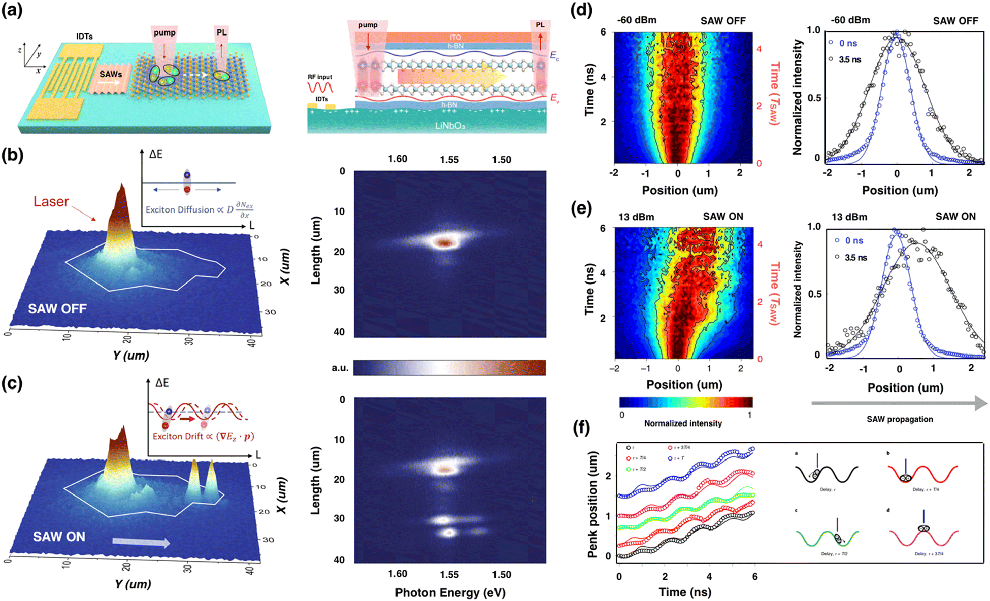 | ||
| Fig. 5 Acoustic exciton transports. (a) Acoustic exciton transport in the monolayer and bilayer WSe2 on the SAW delay lines. The propagating SAWs modulate the exciton energy and transport the excitons away from the pump spot. At the flake edge, the excitons recombine and generate photoluminescence. (b and c) Real-space PL mapping (left) and spectral PL image (right) of the h-BN encapsulated bilayer WSe2 when SAWs (power ∼6 mW) are switched off (b) and on (c). The non-local exciton emission at the flake edge with an emission peak at 1.56 eV is attributed to the IXs in WSe2. After tuning on SAWs, the emission spectrum at the pump spot slightly decreases, while the emission spectrum at the flake edge drastically increases. Two bright emission spots appear at the flake edge and the focal point of two acoustic waves due to the SAW-driven transport of IXs. Reproduced from ref. 92 with permission from Springer Nature, copyright 2022. (d and e) Spatiotemporal mapping of the normalized exciton density (left) and corresponding profiles at different time instances (right) in the monolayer WSe2. The RF input powers are set to −60 dBm (d) and 13 dBm (e) at an optical fluency of 1.2 μJ cm−2. A spatial shift in the exciton density can be observed under RF excitation. At an input power of ∼−60 dBm, the exciton density symmetrically broadens in space due to exciton diffusion in the monolayer. At an input power of ∼13 dBm, an asymmetric spatial shift in the exciton density along the SAW propagation direction is observed and the observed shift increasing with time. (f) Phase-synchronized evolution of the Gaussian peak position extracted by fitting the normalized exciton density. The Gaussian peak position oscillates with the period of SAWs. A progressive delay in the Gaussian peak emerged as the time delay is increased at an increment of T/4. In addition, a net drift in the Gaussian peak aroused along the SAW propagation direction. Reproduced from ref. 91 with permission from Springer Nature, copyright 2022 (Open access). | ||
D. Coherent acoustic phonons
Exciting and manipulating phonons are long-sought goals in the research communities of electronics, information processing, and materials science. Resonant ultrafast excitation of infrared-active phonons (femtosecond pump–probe setup, Fig. 6a) is recognized as a powerful technique in controlling the electronics of 2D materials. With the assistance of this setup, the light-enhanced superconductivity,173–179 ferroelectric polarization,180–183 magnetization,184,185 and ultrafast insulator-to-metal transitions186–191 were unraveled in diverse 2D materials. In addition, coherent phonons in 2D materials could be induced through pumping by intense laser and magnetic fields.192–197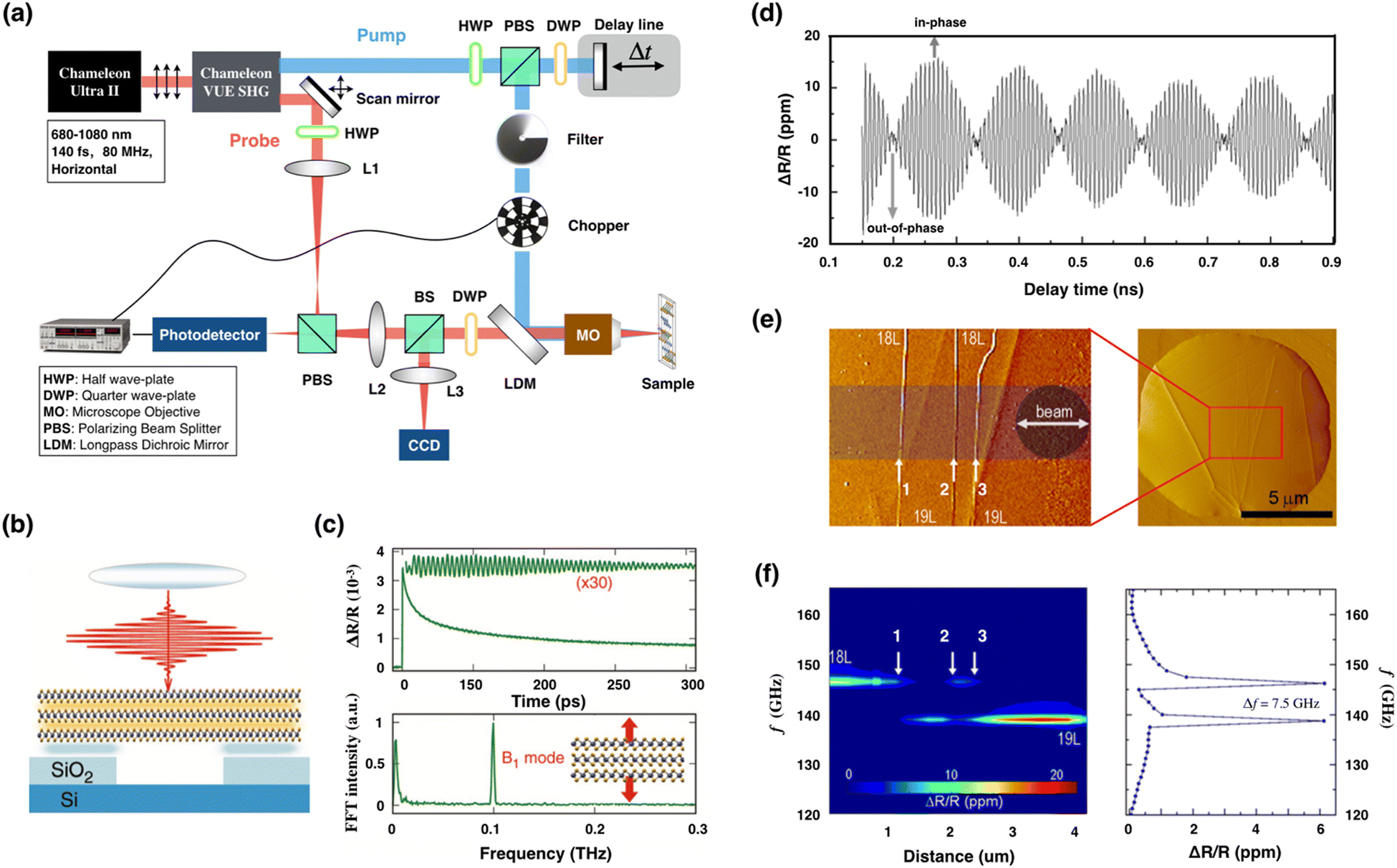 | ||
| Fig. 6 Coherent acoustic phonons. (a) Setup sketch of optical SAW excitation and detection by the femtosecond time-resolved pump–probe technique. The probe beam is sent through a telescope (4f lens) system that consists of an automatically controlled two-axes rotating mirror followed by a confocal convex lens pair and a microscope objective lens, which expands the beam to fill the entire objective aperture for a diffraction-limited probe spot. The rotation axis of the scan mirror is the optical axis. (b) Sketch of a free-standing trilayer MoSe2 flake under incident laser pulses. (c) Transient reflectivity ΔR/R for 22-layer MoSe2 flakes. The filtered signal displaying the coherent acoustic B1 oscillations is shown in the top panel, and the corresponding numerical Fourier transform is depicted below, displaying a clear single peak with a frequency of ∼0.1 THz. Reproduced from ref. 171 with permission from Royal Society of Chemistry, copyright 2019. (d) Transient reflectivity ΔR/R taken at a monolayer step boundary of an 18-layer/19-layer MoS2 suspended film. (e) AFM phase-image showing the monolayer step boundary on the top of MoS2 drum (right). The horizontal dark band shows the path of 1 μm diameter beam across the surface. (f) The corresponding 2D frequency vs. the distance map showing the fast Fourier transform (FFT) spectra of the probe reflectivity, acquired at different positions while stepping the beam across the monolayer steps (e). FFT spectrum of transient reflectivity from (d) that was taken approximately at the 2.2 μm position is shown in the right panel. Reproduced from ref. 172 with permission from Springer Nature, copyright 2021 (Open access). | ||
The resonant optical excitation of infrared-active lattice vibrations is feasible to induce targeted structural deformations in 2D materials.198 In 2016, the temporal dynamics of coherent lattice vibration modes in mono- and few-layer WSe2 flakes was realized by performing time-resolved transmission measurements.199 Under ultrashort pulses resonating with A excitons of the monolayer WSe2, coherent oscillations of A1g optical phonon and longitudinal acoustic phonon at the M point of the Brillouin zone were impulsively generated. Guided by the temperature-dependent evolution of A1g optical phonons, the accelerated phonon dephasing with temperature was modeled by the anharmonic decay process, in which the A1g mode decays into two acoustic modes. In multilayer WSe2 flakes, the interlayer breathing mode (B1) is found to be sensitive to the number of layers, demonstrating its usefulness in characterizing layered TMDCs. Fig. 6b–c show the dynamics of coherent interlayer longitudinal acoustic phonons (B1 mode) for free-standing 2H-MoSe2 flakes with varying thickness from the bilayer to the bulk counterpart.171 From the temporal decay of the phonon modes (frequencies ∼1 THz for the bilayer but decrease to ∼4.2 GHz for the bulk one), it is possible to clearly distinguish an abrupt crossover related to the acoustic mean free path of phonons, and the constraints imposed on the acoustic decay channels during the reduction of film thickness. For thicker MoSe2 flakes (above ∼20 layers), the acoustic attenuations were mainly determined by the scatterings of coherent acoustic modes with thermal phonons through anharmonic three-phonon scattering processes. For flakes thinner than ∼20 layers, the predominant damping mechanism was ascribed to the surface asperity effect. In another report, the Raman-active optical phonon modes of single-layer graphene was experimentally modulated by SAW-induced dynamic strain fields.200 In particular, an effective strain field of 0.24% was generated for single-layer graphene on the LiNbO3 device at a SAW resonator frequency of ∼400 MHz. Under this strain field, the Raman scattering intensity variation of the G band as large as 15% and a phonon frequency shift of up to 10 cm−1 could be achieved. It should be highlighted that this method is universal in manipulating the optical and vibrational properties of other 2D systems.
In order to achieve intense interactions and sideband resolution (single-sideband operation), the SAWs were implemented into exciting high frequency motion and then exploring opto-mechanics with travelling acoustic waves (the regime of stimulated Brillouin scattering).201 In this way, acoustic cavities may offer spatial confinements for high frequency (1–10 GHz) elastic waves and behave as a vital part of opto-mechanical signal processing.202–206 For instance, high frequency (f) and high quality factor (Q) MoS2-based 2D acoustic cavities operating in the frequency range of 50–600 GHz with (f × Q) up to 1 × 10¹⁴ have been reported (Fig. 6d–f). In addition, well-controlled heterogeneities (monolayer steps, drum and interfaces) within the high-quality MoS2 suspended film and a frequency comb generator implemented in the h-BN/MoS2 bilayer can alter the underlying elastic-strain patterns and extend the functionality of acoustic cavities.172 These acoustic cavities in 2D heterostructures provide a pathway for exploring the quantum nature of phonons and developing phonon-based sensing and signal processing platforms.
IV. Conclusion and outlook
In conclusion, we overviewed the SAW-induced emergent phenomena, especially the piezo-electric coupling of SAWs with charge carriers in 2D materials. However, the distortions during mechanical coupling between SAWs and 2D materials may also vary the electronic properties of 2D materials. This could be particularly important since 2D materials could be mounted with emerging phononic structures to localize the SAW displacements for cavity-based sensors.4,207 One feasible direction of 2D materials and SAWs association may lie in sensing, filtrations and fluid controls. The present 2D material toward this direction is a tip of an iceberg, such as graphene, h-BN, MoS2, metal carbides, and metal halides. The interplay of SAWs with other 2D materials is left unexplored. Lastly, a key challenge is how to reproducibly obtain large area and high quality 2D materials on SAW piezo-electric substrates in a straightforward approach. With the joint efforts from materials science, chemistry and optics, we have come to a better position than ever to address the confronted challenges and push the research on interaction of SAWs and 2D materials to a higher level.Conflicts of interest
There are no conflicts to declare.Acknowledgements
This work was supported by the National Natural Science Foundation of China (1210040808), the Natural Science Foundation of Jiangsu Province (BK20210276, BK20210312, and BK20212008), the Postgraduate Research and Practice Innovation Program of NUAA (Grant No. xcxjh20210111), the National Key Research and Development Program of China (2019YFA0705400), the Fundamental Research Funds for the Central Universities (NJ2022002), the Program for Innovative Talents and Entrepreneur in Jiangsu, the Research Fund of State Key Laboratory of Mechanics and Control of Mechanical Structures (MCMS-I-0421K01, and MCMS-I-0422K01), the Fund of Prospective Layout of Scientific Research for NUAA (Nanjing University of Aeronautics and Astronautics) and the Australian Research Council Future Fellowship (FT160100205).References
- G. Zhang, Bulk and Surface Acoustic Waves: Fundamentals, Devices, and Applications, Jenny Stanford Publishing Pte. Ltd., 2022 Search PubMed.
- D. Mandal and S. Banerjee, Sensors, 2022, 22, 820 CrossRef CAS PubMed.
- A. A. Balandin and D. L. Nika, Mater. Today, 2012, 15, 266 CrossRef CAS.
- P. Delsing, A. N. Cleland, M. J. A. Schuetz, J. Knörzer, G. Giedke, J. I. Cirac, K. Srinivasan, M. Wu, K. C. Balram and C. Bäuerle, et al. , J. Phys. D: Appl. Phys., 2019, 52, 353001 CrossRef CAS.
- C. Müller, P. Durdaut, R. B. Holländer, A. Kittmann, V. Schell, D. Meyners, M. Höft, E. Quandt and J. McCord, Adv. Electron. Mater., 2022, 8, 2200033 CrossRef.
- S. Xu, R. Zhang, J. Cui, T. Liu, X. Sui, M. Han, F. Zheng and X. Hu, Micromachines, 2021, 12, 552 CrossRef PubMed.
- S.-Y. Yu, X.-C. Sun, X. Ni, Q. Wang, X.-J. Yan, C. He, X.-P. Liu, L. Feng, M.-H. Lu and Y.-F. Chen, Nat. Mater., 2016, 15, 1243 CrossRef CAS PubMed.
- S. Ban, X. Nie, Z. Lei, J. Yi, A. Vinu, Y. Bao and Y. Liu, Mater. Res. Lett., 2023, 11, 21 CrossRef CAS.
- A. Bienfait, Y. P. Zhong, H.-S. Chang, M.-H. Chou, C. R. Conner, E. Dumur, J. Grebel, G. A. Peairs, R. G. Povey and K. J. Satzinger, et al. , Phys. Rev. X, 2020, 10, 021055 CAS.
- É. Dumur, K. J. Satzinger, G. A. Peairs, M. H. Chou, A. Bienfait, H. S. Chang, C. R. Conner, J. Grebel, R. G. Povey and Y. P. Zhong, et al. , npj Quantum Inform., 2021, 7, 173 CrossRef.
- M. K. Villegas, R. Rasouli and M. Tabrizian, Microsyst. Nanoeng., 2022, 8, 79 CrossRef PubMed.
- P. Zhang, H. Bachman, A. Ozcelik and T. J. Huang, Annu. Rev. Anal. Chem., 2020, 13, 17 CrossRef CAS PubMed.
- X. Ding, P. Li, S.-C. S. Lin, Z. S. Stratton, N. Nama, F. Guo, D. Slotcavage, X. Mao, J. Shi and F. Costanzo, et al. , Lab Chip, 2013, 13, 3626 RSC.
- J.-Q. Wang, Z.-D. Zhang, S.-Y. Yu, H. Ge, K.-F. Liu, T. Wu, X.-C. Sun, L. Liu, H.-Y. Chen and C. He, et al. , Nat. Commun., 2022, 13, 1324 CrossRef CAS PubMed.
- M. J. A. Schuetz, E. M. Kessler, G. Giedke, L. M. K. Vandersypen, M. D. Lukin and J. I. Cirac, Phys. Rev. X, 2015, 5, 031031 Search PubMed.
- R. Manenti, M. J. Peterer, A. Nersisyan, E. B. Magnusson, A. Patterson and P. J. Leek, Phys. Rev. B, 2016, 93, 041411 CrossRef.
- D. A. Golter, T. Oo, M. Amezcua, I. Lekavicius, K. A. Stewart and H. Wang, Phys. Rev. X, 2016, 6, 041060 Search PubMed.
- S. Hong, R. Riedinger, I. Marinkovic, A. Wallucks, S. G. Hofer, R. A. Norte, M. Aspelmeyer and S. Groblacher, Science, 2017, 358, 203 CrossRef CAS PubMed.
- B. A. Moores, L. R. Sletten, J. J. Viennot and K. W. Lehnert, Phys. Rev. Lett., 2018, 120, 227701 CrossRef CAS PubMed.
- S. J. Whiteley, G. Wolfowicz, C. P. Anderson, A. Bourassa, H. Ma, M. Ye, G. Koolstra, K. J. Satzinger, M. V. Holt and F. J. Heremans, et al. , Nat. Phys., 2019, 15, 490 Search PubMed.
- A. Bienfait, K. J. Satzinger, Y. P. Zhong, H.-S. Chang, M.-H. Chou, C. R. Conner, E. Dumur, J. Grebel, G. A. Peairs and R. G. Povey, et al. , Science, 2019, 364, 368 CrossRef CAS PubMed.
- G. Andersson, S. W. Jolin, M. Scigliuzzo, R. Borgani, M. O. Tholen, J. C. Rivera Hernandez, V. Shumeiko, D. B. Haviland and P. Delsing, PRX Quantum, 2022, 3, 010312 CrossRef.
- M. V. Gustafsson, T. Aref, A. F. Kockum, M. K. Ekstrom, G. Johansson and P. Delsing, Science, 2014, 346, 207 CrossRef CAS PubMed.
- R. Manenti, A. F. Kockum, A. Patterson, T. Behrle, J. Rahamim, G. Tancredi, F. Nori and P. J. Leek, Nat. Commun., 2017, 8, 975 CrossRef PubMed.
- Y. Chu, P. Kharel, W. H. Renninger, L. D. Burkhart, L. Frunzio, P. T. Rakich and R. J. Schoelkopf, Science, 2017, 358, 199 CrossRef CAS PubMed.
- K. J. Satzinger, Y. P. Zhong, H. S. Chang, G. A. Peairs, A. Bienfait, M. H. Chou, A. Y. Cleland, C. R. Conner, E. Dumur and J. Grebel, et al. , Nature, 2018, 563, 661 CrossRef CAS PubMed.
- C. Yang, T. Liu, J. Zhu, J. Ren and H. Chen, Phys. Rev. Appl, 2021, 15, 044040 CrossRef CAS.
- M. Yuan, K. Biermann and P. V. Santos, AVS Quantum Sci., 2022, 4, 035901 CrossRef CAS.
- S. A. Tadesse and M. Li, Nat. Commun., 2014, 5, 5402 CrossRef PubMed.
- S. Kapfinger, T. Reichert, S. Lichtmannecker, K. Muller, J. J. Finley, A. Wixforth, M. Kaniber and H. J. Krenner, Nat. Commun., 2015, 6, 8540 CrossRef CAS PubMed.
- M. Li, J. Ling, Y. He, U. A. Javid, S. Xue and Q. Lin, Nat. Commun., 2020, 11, 4123 CrossRef CAS PubMed.
- L. Shao, D. Zhu, M. Colangelo, D. Lee, N. Sinclair, Y. Hu, P. T. Rakich, K. Lai, K. K. Berggren and M. Loncar, Nat. Electron., 2022, 5, 348 CrossRef.
- J. Puebla, Y. Hwang, S. Maekawa and Y. Otani, Appl. Phys. Lett., 2022, 120, 220502 CrossRef CAS.
- S. Maity, L. Shao, S. Bogdanovic, S. Meesala, Y.-I. Sohn, N. Sinclair, B. Pingault, M. Chalupnik, C. Chia and L. Zheng, et al. , Nat. Commun., 2020, 11, 193 CrossRef CAS PubMed.
- D. A. Golter, T. Oo, M. Amezcua, K. A. Stewart and H. Wang, Phys. Rev. Lett., 2016, 116, 143602 CrossRef PubMed.
- W. Fu, Z. Shen, Y. Xu, C. L. Zou, R. Cheng, X. Han and H. X. Tang, Nat. Commun., 2019, 10, 27443 Search PubMed.
- K. S. Novoselov, A. Mishchenko, A. Carvalho and A. H. Castro Neto, Science, 2016, 353, aac9439 CrossRef CAS PubMed.
- J. Pei, J. Yang, T. Yildirim, H. Zhang and Y. Lu, Adv. Mater., 2019, 31, 1706945 CrossRef PubMed.
- P. Zhou, C. Chen, X. Wang, B. Hu and H. San, Sensor. Actuat. A-Phys., 2018, 271, 389 CrossRef CAS.
- Y. Liu, Z. Qiu, A. Carvalho, Y. Bao, H. Xu, S. J. R. Tan, W. Liu, A. H. Castro Neto, K. P. Loh and J. Lu, Nano Lett., 2017, 17, 1970 CrossRef CAS PubMed.
- Y. Liu, J. N. B. Rodrigues, Y. Z. Luo, L. Li, A. Carvalho, M. Yang, E. Laksono, J. Lu, Y. Bao and H. Xu, et al. , Nat. Nanotechnol., 2018, 13, 828 CrossRef CAS PubMed.
- Y. Liu, I. Yudhistira, M. Yang, E. Laksono, Y. Z. Luo, J. Chen, J. Lu, Y. P. Feng, S. Adam and K. P. Loh, Nano Lett., 2018, 18, 3377 CrossRef CAS PubMed.
- E. Zhang, F. Lin, Z. Lei, S. Qi, S. Ban, A. Vinu, J. Yi and Y. Liu, Matter, 2021, 4, 3444 CrossRef CAS.
- Y. Liu, M. Yang, J. Lu, Y. Liu, H. Liu, E. Zhang, W. Fu, J. Wang, Z. Hu and J. Yin, et al. , Chin. Chem. Lett., 2022, 33, 368 CrossRef CAS.
- Y. J. Bae, J. Wang, A. Scheie, J. Xu, D. G. Chica, G. M. Diederich, J. Cenker, M. E. Ziebel, Y. Bai and H. Ren, et al. , Nature, 2022, 609, 282 CrossRef CAS PubMed.
- W. Wu, L. Wang, Y. Li, F. Zhang, L. Lin, S. Niu, D. Chenet, X. Zhang, Y. Hao and T. F. Heinz, Nature, 2014, 514, 470 CrossRef CAS PubMed.
- H. Zhu, Y. Wang, J. Xiao, M. Liu, S. Xiong, Z. J. Wong, Z. Ye, Y. Ye, X. Yin and X. Zhang, Nat. Nanotechnol., 2015, 10, 151 CrossRef CAS PubMed.
- M. M. Alyoruk, Y. Aierken, D. Çakır, F. M. Peeters and C. Sevik, J. Phys. Chem. C, 2015, 119, 23231 CrossRef CAS.
- L. Wei, X. Kuai, Y. Bao, J. Wei, L. Yang, P. Song, M. Zhang, F. Yang and X. Wang, Micromachines, 2021, 12, 724 CrossRef PubMed.
- L. Thevenard, I. S. Camara, J.-Y. Prieur, P. Rovillain, A. Lemaıtre, C. Gourdon and J.-Y. Duquesne, Phys. Rev. B, 2016, 93, 140405 CrossRef.
- M. Foerster, F. Macià, N. Statuto, S. Finizio, A. Hernandez-Mınguez, S. Lendınez, P. V. Santos, J. Fontcuberta, J. M. Hernandez and M. Klaui, et al. , Nat. Commun., 2017, 8, 407 CrossRef PubMed.
- Y. Ishii, R. Sasaki, Y. Nii, T. Ito and Y. Onose, Phys. Rev. Appl, 2018, 9, 034034 CrossRef CAS.
- B. Casals, N. Statuto, M. Foerster, A. Hernández-Mínguez, R. Cichelero, P. Manshausen, A. Mandziak, L. Aballe, J. M. Hernàndez and F. Macià, Phys. Rev. Lett., 2020, 124, 137202 CrossRef CAS PubMed.
- M. Weiler, H. Huebl, F. S. Goerg, F. D. Czeschka, R. Gross and S. T. B. Goennenwein, Phys. Rev. Lett., 2012, 108, 176601 CrossRef CAS PubMed.
- A. Y. Klokov, V. S. Krivobok, A. I. Sharkov and N. Y. Frolov, Sensors, 2022, 22, 870 CrossRef CAS PubMed.
- V. S. Vlasov, A. V. Golov, L. N. Kotov, V. I. Shcheglov, A. M. Lomonosov and V. V. Temnov, Acoust. Phys., 2022, 68, 18 CrossRef.
- H. Zhang, A. Antoncecchi, S. Edward, P. Planken and S. Witte, Phys. Rev. B, 2021, 103, 064303 CrossRef CAS.
- J. Hellemann, F. Müller, M. Msall, P. V. Santos and S. Ludwig, Phys. Rev. Appl, 2022, 17, 044024 CrossRef CAS.
- J. Wang, S. Ota, H. Edlbauer, B. Jadot, P.-A. Mortemousque, A. Richard, Y. Okazaki, S. Nakamura, A. Ludwig and A. D. Wieck, et al. , Phys. Rev. X, 2022, 12, 031035 CAS.
- E. Dumur, K. J. Satzinger, G. A. Peairs, M.-H. Chou, A. Bienfait, H.-S. Chang, C. R. Conner, J. Grebel, R. G. Povey and Y. P. Zhong, et al. , Appl. Phys. Lett., 2019, 114, 223501 CrossRef.
- D. Fall, M. Duquennoy, M. Ouaftouh, N. Smagin, B. Piwakowski and F. Jenot, Sens. Actuators, A, 2018, 273, 303 CrossRef CAS.
- F. J. R. Schulein, E. Zallo, P. Atkinson, O. G. Schmidt, R. Trotta, A. Rastelli, A. Wixforth and H. J. Krenner, Nat. Nanotechnol., 2015, 10, 512 CrossRef PubMed.
- A. Hernández-Mínguez, Y. T. Liou and P. V. Santos, J. Phys. D: Appl. Phys., 2018, 51, 383001 CrossRef.
- G. Wingqvist, Surf. Coat. Technol., 2010, 205, 1279 CrossRef CAS.
- T. Aubert, J. Bardong, O. Legrani, O. Elmazria, M. Assouar, G. Bruckner and A. Talbi, J. Appl. Phys., 2013, 114, 014505 CrossRef.
- S. K. Arya, S. Saha, J. E. Ramirez-Vick, V. Gupta, S. Bhansali and S. P. Singh, Anal. Chim. Acta, 2012, 737, 1 CrossRef CAS PubMed.
- N. Harris, M. Hill, R. Torah, R. Townsend, S. Beeby, N. White and J. Ding, Sens. Actuators, A, 2006, 132, 311 CrossRef CAS.
- M. Endo, S. Kimura, S. Tani and Y. Kobayashi, Commun. Phys., 2021, 4, 73 CrossRef CAS.
- P. Liu, K. Yi, Y. Park and H. Sohn, Opt. Laser. Eng., 2022, 150, 106844 CrossRef.
- O. Matsuda, M. C. Larciprete and O. B. Wright, Ultrasonics, 2015, 56, 3 CrossRef CAS PubMed.
- H. Takahashi, T. Omori and K. Hashimoto, Jpn. J. Appl. Phys., 2021, 60, SDDC10 CrossRef CAS.
- K. Kawai, H. Takahashi, T. Omori and K. Hashimoto, Jpn. J. Appl. Phys., 2022, 61, SG1012 CrossRef.
- T. Tachizaki, T. Muroya, O. Matsuda, Y. Sugawara, D. H. Hurley and O. B. Wright, Rev. Sci. Instrum., 2006, 77, 043713 CrossRef.
- L. Shao, V. J. Gokhale, B. Peng, P. Song, J. Cheng, J. Kuo, A. Lal, W.-M. Zhang and J. J. Gorman, Nat. Commun., 2022, 13, 694 CrossRef CAS PubMed.
- K. Kokkonen and M. Kaivola, Appl. Phys. Lett., 2008, 92, 063502 CrossRef.
- Y. Hong, S. D. Sharples, M. Clark and M. G. Somekh, Appl. Phys. Lett., 2003, 83, 3260 CrossRef CAS.
- J. Higuet, T. Valier-Brasier, T. Dehoux and B. Audoin, Rev. Sci. Instrum., 2011, 82, 114905 CrossRef PubMed.
- C. Chang, W. Chen, Y. Chen, Y. Chen, Y. Chen, F. Ding, C. Fan, H. J. Fan, Z. Fan and C. Gong, et al. , Acta Phys. -Chim. Sin., 2021, 37, 2108017 Search PubMed.
- K. F. Mak and J. Shan, Nat. Photon., 2016, 10, 216 CrossRef CAS.
- S. Yang, Y. Chen and C. Jiang, InfoMat, 2021, 3, 397 CrossRef.
- V. Miseikis, J. E. Cunningham, K. Saeed, R. O’Rorke and A. G. Davies, Appl. Phys. Lett., 2012, 100, 133105 CrossRef.
- L. Bandhu, L. M. Lawton and G. R. Nash, Appl. Phys. Lett., 2013, 103, 133101 CrossRef.
- L. Bandhu and G. R. Nash, Appl. Phys. Lett., 2014, 105, 263106 CrossRef.
- T. Poole and G. R. Nash, J. Phys. D: Appl. Phys., 2018, 51, 154001 CrossRef.
- T. Matsushita, T. Mizushima, I. Vekhter and S. Fujimoto, Phys. Rev. B, 2022, 105, 134520 CrossRef CAS.
- P. O. Sukhachov and H. Rostami, Phys. Rev. Lett., 2020, 124, 126602 CrossRef CAS PubMed.
- P. Zhao, C. H. Sharma, R. Liang, C. Glasenapp, L. Mourokh, V. M. Kovalev, P. Huber, M. Prada, L. Tiemann and R. H. Blick, Phys. Rev. Lett., 2022, 128, 256601 CrossRef CAS PubMed.
- P. Bhalla, G. Vignale and H. Rostami, Phys. Rev. B, 2022, 105, 125407 CrossRef CAS.
- K. Datta, Z. Li, Z. Lyu and P. B. Deotare, ACS Nano, 2021, 15, 12334 CrossRef CAS PubMed.
- D. Scolfaro, M. Finamor, L. O. Trinchaõ, B. L. T. Rosa, A. Chaves, P. V. Santos, F. Iikawa and O. D. D. Couto, ACS Nano, 2021, 15, 15371 CrossRef CAS PubMed.
- R. Peng, A. Ripin, Y. Ye, J. Zhu, C. Wu, S. Lee, H. Li, T. Taniguchi, K. Watanabe and T. Cao, et al. , Nat. Commun., 2022, 1, 1334 CrossRef PubMed.
- K. Datta, Z. Lyu, Z. Li, T. Taniguchi, K. Watanabe and P. B. Deotare, Nat. Photon., 2022, 16, 242 CrossRef CAS.
- K. Sonowal, D. V. Boev, A. V. Kalameitsev, V. M. Kovalev and I. G. Savenko, Phys. Rev. B, 2022, 106, 155426 CrossRef.
- A. V. Kalameitsev, V. M. Kovalev and I. G. Savenko, Phys. Rev. Lett., 2019, 122, 256801 CrossRef CAS PubMed.
- K. Sonowal, A. V. Kalameitsev, V. M. Kovalev and I. G. Savenko, Phys. Rev. B, 2020, 102, 235405 CrossRef CAS.
- T. Kawada, M. Kawaguchi, T. Funato, H. Kohno and M. Hayashi, Sci. Adv., 2021, 7, eabd9697 CrossRef CAS PubMed.
- L. Bandhu and G. R. Nash, Nano Res., 2016, 9, 685 CrossRef CAS.
- E. Preciado, F. J. R. Schülein, A. E. Nguyen, D. Barroso, M. Isarraraz, G. von Son, I.-H. Lu, W. Michailow, B. Möller and V. Klee, et al. , Nat. Commun., 2015, 6, 8593 CrossRef CAS PubMed.
- S. Zheng, E. Wu, Z. Feng, R. Zhang, Y. Xie, Y. Yu, R. Zhang, Q. Li, J. Liu and W. Pang, et al. , Nanoscale, 2018, 10, 10148 RSC.
- M. Yokoi, S. Fujiwara, T. Kawamura, T. Arakawa, K. Aoyama, H. Fukuyama, K. Kobayashi and Y. Niimi, Sci. Adv., 2020, 6, eaba1377 CrossRef CAS PubMed.
- S. Nafees, S. S. Z. Ashraf and M. Obaidurrahman, Phys. Scr., 2022, 97, 045705 CrossRef.
- V. I. Fal’ko, S. V. Meshkov and S. V. Iordanskii, Phys. Rev. B: Condens. Matter Mater. Phys., 1993, 47, 9910 CrossRef PubMed.
- M. Rotter, A. Wixforth, W. Ruile, D. Bernklau and H. Riechert, Appl. Phys. Lett., 1998, 73, 2128 CrossRef CAS.
- T.-K. Hsiao, A. Rubino, Y. Chung, S.-K. Son, H. Hou, J. Pedrós, A. Nasir, G. Éthier-Majcher, M. J. Stanley and T. Phillips, et al. , Nat. Commun., 2020, 11, 917 CrossRef CAS PubMed.
- Z. Insepov, E. Emelin, O. Kononenko, D. V. Roshchupkin, K. B. Tnyshtykbayev and K. A. Baigarin, Appl. Phys. Lett., 2015, 106, 023505 CrossRef.
- S. O. Yurchenko, K. A. Komarov and V. I. Pustovoit, AIP Adv., 2015, 5, 057144 CrossRef.
- K. B. Tynyshtykbaev and Z. Insepov, Nano Express, 2021, 2, 020016 CrossRef.
- P. Zhao, L. Tiemann, H. K. Trieu and R. H. Blick, Appl. Phys. Lett., 2020, 116, 103102 CrossRef CAS.
- J. Schiefele, J. Pedrós, F. Sols, F. Calle and F. Guinea, Phys. Rev. Lett., 2013, 111, 237405 CrossRef PubMed.
- X. Wang, J. Ji, P. Yang, X. Li, Y. Pang and P. Lu, Talanta, 2022, 243, 123328 CrossRef CAS PubMed.
- I. G. Savenko, A. V. Kalameitsev, L. G. Mourokh and V. M. Kovalev, Phys. Rev. B, 2020, 102, 045407 CrossRef CAS.
- C.-C. Hsu, M. L. Teague, J.-Q. Wang and N.-C. Yeh, Adv. Sci., 2020, 6, eaat9488 CrossRef CAS PubMed.
- S.-Y. Li, Y. Su, Y.-N. Ren and L. He, Phys. Rev. Lett., 2020, 124, 106802 CrossRef CAS PubMed.
- D.-H. Kang, H. Sun, M. Luo, K. Lu, M. Chen, Y. Kim, Y. Jung, X. Gao, S. J. Parluhutan and J. Ge, et al. , Nat. Commun., 2021, 12, 5087 CrossRef CAS PubMed.
- A. A. Herasymchuk, P. O. Sukhachov and E. V. Gorbar, Phys. Rev. B, 2022, 106, 045132 CrossRef CAS.
- F. Guinea, M. I. Katsnelson and A. K. Geim, Nat. Phys., 2010, 6, 30 Search PubMed.
- E. Sela, Y. Bloch, F. von Oppen and M. B. Shalom, Phys. Rev. Lett., 2020, 124, 026602 CrossRef CAS PubMed.
- A. R. Rezk, B. Carey, A. F. Chrimes, D. W. M. Lau, B. C. Gibson, C. Zheng, M. S. Fuhrer, L. Y. Yeo and K. Kalantarzadeh, Nano Lett., 2016, 16, 849 CrossRef CAS PubMed.
- M. Yuan, A. Hernández-Mínguez, K. Biermann and P. V. Santos, Phys. Rev. B, 2018, 98, 155311 CrossRef CAS.
- M. Yuan, K. Biermann, S. Takada, C. Bäuerle and P. V. Santos, ACS Photonics, 2021, 8, 758 CrossRef CAS.
- A. R. Rezk, S. Walia, R. Ramanathan, H. Nili, J. Z. Ou, V. Bansal, J. R. Friend, M. Bhaskaran, L. Y. Yeo and R. Sriram, Adv. Opt. Mater., 2015, 3, 888 CrossRef CAS.
- T. Huang, P. Han, X. Wang, J. Ye, W. Sun, S. Feng and Y. Zhang, J. Phys. D: Appl. Phys., 2017, 50, 114005 CrossRef.
- L. Sheng, G. Tai, Y. Yin, C. Hou and Z. Wu, Adv. Opt. Mater., 2021, 9, 2001349 CrossRef CAS.
- R. Fandan, J. Pedrós and F. Calle, ACS Photonics, 2021, 8, 1698 CrossRef CAS.
- A. Hernández-Mínguez, A. V. Poshakinskiy, M. Hollenbach, P. V. Santos and G. V. Astakhov, Sci. Adv., 2021, 7, eabj5030 CrossRef PubMed.
- F. Iikawa, A. Hernández-Mínguez, I. Aharonovich, S. Nakhaie, Y. T. Liou, J. M. J. Lopes and P. V. Santos, Appl. Phys. Lett., 2019, 114, 171104 CrossRef.
- P. Qi, Y. Dai, Y. Luo, G. Tao, W. Qian, Z. Zhang, Z. Zhang, T. H. Zhang, L. Lin and W. Liu, et al. , Adv. Mater. Technol., 2022, 2022, 2200032 CrossRef.
- J. R. Schaibley, H. Yu, G. Clark, P. Rivera, J. S. Ross, K. L. Seyler, W. Yao and X. Xu, Nat. Rev. Mater., 2016, 1, 16055 CrossRef CAS.
- P. Rivera, H. Yu, K. L. Seyler, N. P. Wilson, W. Yao and X. Xu, Nat. Nanotechnol., 2018, 13, 1004 CrossRef CAS PubMed.
- M. Kulig, J. Zipfel, P. Nagler, S. Blanter, C. Schuller, T. Korn, N. Paradiso, M. M. Glazov and A. Chernikov, Phys. Rev. Lett., 2018, 120, 207401 CrossRef CAS PubMed.
- J. Rudolph, R. Hey and P. V. Santos, Phys. Rev. Lett., 2007, 99, 047602 CrossRef.
- S. Lazic, A. Violante, K. Cohen, R. Hey, R. Rapaport and P. V. Santos, Phys. Rev. B: Condens. Matter Mater. Phys., 2014, 89, 085313 CrossRef.
- M. G. Harats, J. N. Kirchhof, M. Qiao, K. Greben and K. I. Bolotin, Nat. Photon., 2020, 14, 324 CrossRef CAS.
- R. Rosati, R. Schmidt, S. Brem, R. Perea-Causın, I. Niehues, J. Kern, J. A. Preuß, R. Schneider, S. Michaelis de Vasconcellos and R. Bratschitsch, et al. , Nat. Commun., 2021, 12, 7221 CrossRef CAS PubMed.
- S. Z. Uddin, N. Higashitarumizu, H. Kim, J. Yi, X. Zhang, D. Chrzan and A. Javey, ACS Nano, 2022, 16, 8005 CrossRef CAS PubMed.
- D. F. Cordovilla Leon, Z. Li, S. W. Jang, C.-H. Cheng and P. B. Deotare, Appl. Phys. Lett., 2018, 113, 252101 CrossRef.
- H. Moon, G. Grosso, C. Chakraborty, C. Peng, T. Taniguchi, K. Watanabe and D. Englund, Nano Lett., 2020, 20, 6791 CrossRef CAS PubMed.
- Z. Huang, Y. Liu, K. Dini, Q. Tan, Z. Liu, H. Fang, J. Liu, T. Liew and W. Gao, Nano Lett., 2020, 20, 1345 CrossRef CAS PubMed.
- S. Z. Uddin, H. Kim, M. Lorenzon, M. Yeh, D.-H. Lien, E. S. Barnard, H. Htoon, A. Weber-Bargioni and A. Javey, ACS Nano, 2020, 14, 13433 CrossRef CAS PubMed.
- D. Unuchek, A. Ciarrocchi, A. Avsar, K. Watanabe, T. Taniguchi and A. Kis, Nature, 2018, 560, 340 CrossRef CAS PubMed.
- L. A. Jauregui, A. Y. Joe, K. Pistunova, D. S. Wild, A. A. High, Y. Zhou, G. Scuri, K. D. Greve, A. Sushko and C.-H. Yu, et al. , Science, 2019, 366, 870 CrossRef CAS PubMed.
- L. H. Fowler-Gerace, D. J. Choksy and L. V. Butov, Phys. Rev. B, 2021, 104, 165302 CrossRef CAS.
- S. Deng, E. Shi, L. Yuan, L. Jin, L. Dou and L. Huang, Nat. Commun., 2020, 11, 664 CrossRef CAS PubMed.
- E. Penzo, A. Loiudice, E. S. Barnard, N. J. Borys, M. J. Jurow, M. Lorenzon, I. Rajzbaum, E. K. Wong, Y. Liu and A. M. Schwartzberg, et al. , ACS Nano, 2020, 14, 6999 CrossRef CAS PubMed.
- N. Kumar, Q. Cui, F. Ceballos, D. He, Y. Wang and H. Zhao, Nanoscale, 2014, 6, 4915 RSC.
- L. Yuan and L. Huang, Nanoscale, 2015, 7, 7402 RSC.
- D. Unuchek, A. Ciarrocchi, A. Avsar, Z. Sun, K. Watanabe, T. Taniguchi and A. Kis, Nat. Nanotechnol., 2019, 14, 1104 CrossRef CAS PubMed.
- M. Shimasaki, T. Nishihara, K. Matsuda, T. Endo, Y. Takaguchi, Z. Liu, Y. Miyata and Y. Miyauchi, ACS Nano, 2022, 16, 8205 CrossRef CAS PubMed.
- W. Yao, D. Yang, Y. Chen, J. Hu, J. Li and D. Li, Nano Lett., 2022, 22, 7230 CrossRef CAS PubMed.
- J. Choi, W.-T. Hsu, L.-S. Lu, L. Sun, H.-Y. Cheng, M. H. Lee, J. Quan, K. Tran, C.-Y. Wang and M. Staab, et al. , Sci. Adv., 2020, 6, eaba8866 CrossRef CAS PubMed.
- A. A. High, A. T. Hammack, L. V. Butov, M. Hanson and A. C. Gossard, Opt. Lett., 2007, 32, 2466 CrossRef CAS PubMed.
- L. Cognet, D. A. Tsyboulski, J.-D. R. Rocha, C. D. Doyle, J. M. Tour and R. B. Weisman, Science, 2007, 316, 1465 CrossRef CAS PubMed.
- S. Moritsubo, T. Murai, T. Shimada, Y. Murakami, S. Chiashi, S. Maruyama and Y. K. Kato, Phys. Rev. Lett., 2010, 104, 247402 CrossRef CAS PubMed.
- P. Rivera, K. L. Seyler, H. Yu, J. R. Schaibley, J. Yan, D. G. Mandrus, W. Yao and X. Xu, Science, 2016, 351, 688 CrossRef CAS PubMed.
- L. Yuan, B. Zheng, J. Kunstmann, T. Brumme, A. B. Kuc, C. Ma, S. Deng, D. Blach, A. Pan and L. Huang, Nat. Mater., 2020, 19, 617 CrossRef CAS PubMed.
- S. Park, D. Kim and M. K. Seo, ACS Photonics, 2021, 8, 3619 CrossRef CAS.
- E. Barré, O. Karni, E. Liu, A. L. O’Beirne, X. Chen, H. B. Ribeiro, L. Yu, B. Kim, K. Watanabe and T. Taniguchi, et al. , Science, 2022, 376, 406 CrossRef PubMed.
- E. C. Regan, D. Wang, E. Y. Paik, Y. Zeng, L. Zhang, J. Zhu, A. H. MacDonald, H. Deng and F. Wang, Nat. Rev. Mater., 2022, 7, 778 CrossRef CAS.
- D. Huang, J. Choi, C.-K. Shih and X. Li, Nat. Nanotechnol., 2022, 17, 227 CrossRef CAS PubMed.
- H. Lee, Y. Koo, J. Choi, S. Kumar, H.-T. Lee, G. Ji, S. H. Choi, M. Kang, K. K. Kim and H.-R. Park, et al. , Sci. Adv., 2022, 8, eabm5236 CrossRef CAS PubMed.
- F. Dirnberger, J. D. Ziegler, P. E. Faria Junior, R. Bushati, T. Taniguchi, K. Watanabe, J. Fabian, D. Bougeard, A. Chernikov and V. M. Menon, Sci. Adv., 2021, 7, eabj3066 CrossRef CAS PubMed.
- L. H. Fowler-Gerace, Z. Zhou, E. A. Szwed and L. V. Butov, arXiv:2204.09760.
- X. Hong, J. Kim, S.-F. Shi, Y. Zhang, C. Jin, Y. Sun, S. Tongay, J. Wu, Y. Zhang and F. Wang, Nat. Nanotechnol., 2014, 9, 682 CrossRef CAS PubMed.
- P. Merkl, F. Mooshammer, P. Steinleitner, A. Girnghuber, K. Q. Lin, P. Nagler, J. Holler, C. Schuller, J. M. Lupton and T. Korn, et al. , Nat. Mater., 2019, 18, 691 CrossRef CAS PubMed.
- A. Chaves, J. G. Azadani, H. Alsalman, D. R. da Costa, R. Frisenda, A. J. Chaves, S. H. Song, Y. D. Kim, D. He and J. Zhou, et al. , npj 2D Mater. Appl., 2020, 4, 29 CrossRef CAS.
- D. N. Shanks, F. Mahdikhanysarvejahany, T. G. Stanfill, M. R. Koehler, D. G. Mandrus, T. Taniguchi, K. Watanabe, B. J. LeRoy and J. R. Schaibley, Nano Lett., 2022, 22, 6599 CrossRef CAS PubMed.
- A. Violante, K. Cohen, S. Lazic, R. Hey, R. Rapaport and P. V. Santos, New J. Phys., 2014, 16, 033035 CrossRef CAS.
- K. He, N. Kumar, L. Zhao, Z. Wang, K. F. Mak, H. Zhao and J. Shan, Phys. Rev. Lett., 2014, 113, 026803 CrossRef CAS PubMed.
- A. Chernikov, T. C. Berkelbach, H. M. Hill, A. Rigosi, Y. Li, O. B. Aslan, D. R. Reichman, M. S. Hybertsen and T. F. Heinz, Phys. Rev. Lett., 2014, 113, 076802 CrossRef CAS PubMed.
- C. Schneider, M. M. Glazov, T. Korn, S. Hofling and B. Urbaszek, Nat. Commun., 2018, 9, 2695 CrossRef PubMed.
- P. Soubelet, A. A. Reynoso, A. Fainstein, K. Nogajewski, M. Potemski, C. Faugeras and A. E. Bruchhausen, Nanoscale, 2019, 11, 10446 RSC.
- M. K. Zalalutdinov, J. T. Robinson, J. J. Fonseca, S. W. LaGasse, T. Pandey, L. R. Lindsay, T. L. Reinecke, D. M. Photiadis, J. C. Culbertson and C. D. Cress, et al. , Nat. Commun., 2021, 12, 3267 CrossRef CAS PubMed.
- M. Budden, T. Gebert, M. Buzzi, G. Jotzu, E. Wang, T. Matsuyama, G. Meier, Y. Laplace, D. Pontiroli and M. Riccò, et al. , Nat. Phys., 2021, 17, 611 Search PubMed.
- J. Demsar, J. Low Temp. Phys., 2020, 201, 676 CrossRef CAS.
- S. Kaiser, Phys. Scr., 2017, 92, 103001 CrossRef.
- R. Mankowsky, M. Först and A. Cavalleri, Rep. Prog. Phys., 2016, 70, 064503 CrossRef PubMed.
- M. Mitrano, A. Cantaluppi, D. Nicoletti, S. Kaiser, A. Perucchi, S. Lupi, P. Di Pietro, D. Pontiroli, M. Ricco and S. R. Clark, et al. , Nature, 2016, 530, 461 CrossRef CAS PubMed.
- R. Mankowsky, A. Subedi, M. Först, S. O. Mariager, M. Chollet, H. T. Lemke, J. S. Robinson, J. M. Glownia, M. P. Minitti and A. Frano, et al. , Nature, 2014, 516, 71 CrossRef CAS PubMed.
- D. Fausti, R. I. Tobey, N. Dean, S. Kaiser, A. Dienstm, M. C. Hoffmann, S. Pyon, T. Takayama, H. Takagi and A. Cavalleri, Science, 2011, 331, 189 CrossRef CAS PubMed.
- R. Mankowsky, A. von Hoegen, M. Först and A. Cavalleri, Phys. Rev. Lett., 2017, 118, 197601 CrossRef CAS PubMed.
- T. F. Nova, A. S. Disa, M. Fechner and A. Cavalleri, Science, 2019, 364, 1075 CrossRef CAS PubMed.
- X. Li, T. Qiu, J. Zhang, E. Baldini, J. Lu, A. M. Rappe and K. A. Nelson, Science, 2019, 364, 1079 CrossRef CAS PubMed.
- D. Shin, S. A. Sato, H. Hübener, U. De Giovannini, N. Park and A. Rubio, npj Comput. Mater., 2020, 6, 182 CrossRef CAS.
- D. Afanasiev, J. R. Hortensius, B. A. Ivanov, A. Sasani, E. Bousquet, Y. M. Blanter, R. V. Mikhaylovskiy, A. V. Kimel and A. D. Caviglia, Nat. Mater., 2021, 20, 607 CrossRef CAS PubMed.
- A. Stupakiewicz, C. S. Davies, K. Szerenos, D. Afanasiev, K. S. Rabinovich, A. V. Boris, A. Caviglia, A. V. Kimel and A. Kirilyuk, Nat. Phys., 2021, 17, 489 Search PubMed.
- E. Baldini, T. Kubacka, B. P. P. Mallett, C. Ma, S. M. Koohpayeh, Y. Zhu, C. Bernhard, S. L. Johnson and F. Carbone, Phys. Rev. B, 2018, 97, 125149 CrossRef CAS.
- D. Werdehausen, T. Takayama, M. Hoppner, G. Albrecht, A. W. Rost, Y. Lu, D. Manske, T. Takagi and S. Kaiser, Sci. Adv., 2018, 4, 1734 Search PubMed.
- A. de la Torre, D. M. Kennes, M. Claassen, S. Gerber, J. W. McIver and M. A. Sentef, Rev. Mod. Phys., 2021, 93, 041002 CrossRef CAS.
- R. J. Kirby, L. Muechler, S. Klemenz, C. Weinberg, A. Ferrenti, M. Oudah, D. Fausti, G. D. Scholes and L. M. Schoop, Phys. Rev. B, 2021, 103, 205138 CrossRef CAS.
- Q. M. Liu, D. Wu, Z. A. Li, L. Y. Shi, Z. X. Wang, S. J. Zhang, T. Lin, T. C. Hu, H. F. Tian and J. Q. Li, et al. , Nat. Commun., 2021, 12, 2050 CrossRef CAS PubMed.
- H. M. Bretscher, P. Andrich, P. Telang, A. Singh, L. Harnagea, A. K. Sood and A. Rao, Nat. Commun., 2021, 12, 1699 CrossRef CAS PubMed.
- I. Esin, I. Esterlis, E. Demler and G. Refael, 2022, arXiv: 2207.11245v1.
- C. P. Weber, J. Appl. Phys., 2021, 129, 070901 CrossRef CAS.
- S. Mor, V. Gosetti, A. Molina-Sánchez, D. Sangalli, S. Achilli, V. F. Agekyan, P. Franceschini, C. Giannetti, L. Sangaletti and S. Pagliara, Phys. Rev. Res., 2021, 3, 043175 CrossRef CAS.
- D. Li, C. Trovatello, S. Dal Conte, M. Nuß, G. Soavi, G. Wang, A. C. Ferrari, G. Cerullo and T. Brixner, Nat. Commun., 2021, 12, 954 CrossRef CAS PubMed.
- C. Trovatello, H. P. C. Miranda, A. Molina-Sánchez, R. Borrego-Varillas, C. Manzoni, L. Moretti, L. Ganzer, M. Maiuri, J. Wang and D. Dumcenco, et al. , ACS Nano, 2020, 14, 5700 CrossRef CAS PubMed.
- K. Shinokita, K. Reimann, M. Woerner, T. Elsaesser, R. Hey and C. Flytzanis, Phys. Rev. B, 2016, 116, 075504 Search PubMed.
- M. Henstridge, M. Först, E. Rowe, M. Fechner and A. Cavalleri, Nat. Phys., 2022, 18, 457 Search PubMed.
- T. Y. Jeong, B. M. Jin, S. H. Rhim, L. Debbichi, J. Park, Y. D. Jang, H. R. Lee, D.-H. Chae, D. Lee and Y.-H. Kim, et al. , ACS Nano, 2016, 10, 5560 CrossRef CAS PubMed.
- R. Fandan, J. Pedrós, A. Hernández-Mínguez, F. Iikawa, P. V. Santos, A. Boscá and F. Calle, Nano Lett., 2020, 20, 402 CrossRef CAS PubMed.
- R. Van Laer, R. Baets and D. Van Thourhout, Phys. Rev. A, 2016, 93, 053828 CrossRef.
- K. Fang, M. H. Matheny, X. Luan and O. Painter, Nat. Photon., 2016, 10, 489 CrossRef CAS.
- L. Shao, S. Maity, L. Zheng, L. Wu, A. Shams-Ansari, Y.-I. Sohn, E. Puma, M. Gadalla, M. Zhang and C. Wang, et al. , Phys. Rev. Appl, 2019, 12, 014022 CrossRef CAS.
- M. Forsch, R. Stockill, A. Wallucks, I. Marinkovic, C. Gärtner, R. A. Norte, F. van Otten, A. Fiore, K. Srinivasan and S. Gröblacher, Nat. Phys., 2020, 16, 69 Search PubMed.
- A. Wallucks, I. Marinkovic, B. Hensen, R. Stockill and S. Groblacher, Nat. Phys., 2020, 16, 772 Search PubMed.
- Z.-Z. Zhang, X.-X. Song, G. Luo, Z.-J. Su, K.-L. Wang, G. Cao, H.-O. Li, M. Xiao, G.-C. Guo and L. Tian, et al. , Proc. Natl. Acad. Sci. U. S. A., 2020, 117, 5582 CrossRef CAS PubMed.
- B. J. Ash, S. R. Worsfold, P. Vukusic and G. R. Nash, Nat. Commun., 2017, 8, 174 CrossRef CAS PubMed.
| This journal is © The Royal Society of Chemistry 2023 |