
Inverted perovskite solar cells based on potassium salt-modified NiOX hole transport layers†
Xinyi
Liu
,
Hong Wei
Qiao
,
Mengjiong
Chen
,
Bing
Ge
,
Shuang
Yang
 *,
Yu
Hou
* and
Hua Gui
Yang
*,
Yu
Hou
* and
Hua Gui
Yang
Key Laboratory for Ultrafine Materials of Ministry of Education, Shanghai Engineering Research Center of Hierarchical Nanomaterials, School of Materials Science and Engineering, East China University of Science and Technology, Shanghai 200237, China. E-mail: syang@ecust.edu.cn; yhou@ecust.edu.cn
First published on 1st February 2021
Abstract
Perovskite solar cells (PSCs) have been attracting increasing attention in recent years because of their exceptional high efficiency with incredible developments. However, the poor contact between the hole transport layer (HTL) and perovskite layer still limits the further development of power conversion efficiency (PCE) for inverted solar cells, particularly for inorganic HTL based devices. Herein, potassium salt (KI, KSCN and KNO3) modified nickel oxides are selected as HTLs to improve the photovoltaic performance of an inverted device. We found that all potassium salts play positive roles in optimizing the photovoltaic parameters. Through the modification of potassium salts, higher charge recombination impedance and strong photoluminescence quenching were achieved, which means retarded carrier nonradiative recombination and quick charge transfer at the interface. Besides, KI modified NiOX could improve the perovskite film coverage and reduce trap densities. Thus, the champion device based on a KI modified NiOX film attained a PCE of 20.10% with an enhanced fill factor of 0.812. The findings demonstrate that potassium doping is an effective route to improve the performance of inverted planar PSCs.
Introduction
Organometal halide perovskites have attracted plenty of attention in solar cells, light-emitting diodes (LEDs), lasers, detectors and other fields due to their excellent performance.1–6 As a light absorption material, the application of perovskites has developed rapidly in the field of photovoltaics. In particular, the power conversion efficiencies (PCEs) of perovskite solar cells (PSCs) have been increased from 3.8%7 in 2009 to the current world record of 25.5%.8 Perovskite materials represent both n-type and p-type characteristics, which provides a basis for the diversity of solar cell structure.9 Generally, the structure of PSCs is divided into two categories. In conventional devices, mesoporous or compact n-type oxide semiconducting materials work as an electron transport layer (ETL) deposited on conducting substrates under the light absorber layer, and a hole transport layer (HTL) acts as the p-type contact to collect holes on the top. Alternatively, the n- and p-type transport layers are fabricated in the reverse sequence for the inverted structure.10 Although the conventional PSCs demonstrate higher PCEs than the inverted PSCs, conventional efficient solar cells usually require a mesoporous titanium oxide ETL as a support layer for electron transport, which causes complicated assembly processes and UV-induced degradation of perovskite.11–13 Small molecules,14–16 such as 2,2′,7,7′-tetrakis[N,N-di(4-methoxyphenyl)amino]-9,9′-spirobifluorene (spiro-OMeTAD), have been used as a benchmark HTL for conventional PSCs, in which Li and Co salts also hamper the device stability.17–19 Moreover, its cost is about 5 times more than that of gold, which would significantly limit the commercialization of PSCs. Therefore, it is critical to search for other low-cost and efficient hole transport materials to replace expensive spiro-OMeTAD. Herein, we took inverted PSCs as the main research object and explored the influence of different HTLs.Poly(3,4-ethylenedioxythiophene)-poly(styrenesulfonate) (PEDOT:PSS) is a widespread hole transport material in inverted devices,20 but its hydroscopicity and high acidity have a serious negative impact on device stability. In this regard, different inorganic hole transport materials are considered to replace PEDOT:PSS.21–23 Nickel oxide is one of the most popular inorganic HTL materials due to its prominent properties such as high optical transmittance, appropriate work function and lower valence band position.24 Unfortunately, the PCEs of the inverted PSCs based on a nickel oxide HTL have been greatly improved, but are still lower than those of conventional structure devices.25,26 This is mainly induced by the inferior crystallinity of perovskite and the poor contact between the HTLs and perovskite layers. Interface modification is a simple and efficient way to facilitate the contact and charge transfer, so as to obtain better device performance.27 Yang et al.28 modified a nickel oxide layer by a sol–gel method with diethanolamine (DEA) to promote the interface contact and perovskite crystallinity. As a result, the PCE was significantly lifted from 11.2 to 15.9%. In addition to the small molecular modification, a buffer layer is also constructed to reduce carrier recombination at the interface.29,30 For instance, introducing an aluminum oxide buffer layer, the device showed less interface carrier recombination and surface defects of the perovskite layer, thus enhancing the device performance.10 In addition, treatment with metal ions in the perovskite layer is competent for passivating perovskite crystal defects and improving device performance.31–33 In particular, on adding potassium ions to a perovskite layer, both the charge transport and hysteresis are optimized.34 However, few reports have researched these metal salts directly at the interface,35,36 where the majority of defects exist.
In this work, we developed inverted structure PSCs with inorganic potassium salt modified NiOX as the HTL. The devices after interface modification achieved optimized photovoltaic parameters. The inverted PSCs using KI treatment exhibited a champion PCE of 20.10% with a high fill factor (FF) of 0.812. This finding provides an effective strategy to fabricate high efficiency inverted PSCs.
Results and discussion
To understand the potential influence on morphology of introducing potassium salts (KI, KSCN and KNO3), we performed scanning electron microscopy (SEM) and measurements of NiOX thin films with or without modification. As shown in Fig. 1a–d, all NiOX films are uniform and have no obvious change after modification of all potassium salts. Then CH3NH3PbI3 perovskite films were formed by a two-step continuous spin-coating and annealing procedure.37 Compared with a pristine sample, Fig. 1e–h display that the perovskite films based on modified NiOX films have fewer holes and better surface coverage. Comparable research on HTLs has also suggested that small amounts of metal salt could smooth the NiOX films, promoting the formation of highly crystalline, uniform perovskite layers,38,39 which is consistent with the observations in the atomic force microscopy (AFM) images (Fig. S1, ESI†). This is certainly devoted to optimizing the photoexcited charge carrier generation and transportation. To further investigate the crystal structures of the perovskite films prepared by a two-step continuous method, we employed X-ray diffraction (XRD) to characterize the HTL/PbI2 and HTL/Perovskite films (Fig. 2a and b). The peak positions of PbI2 are nearly identical deposited on various samples with and without potassium salt modification. Meanwhile, the main diffraction peaks at 2θ = 14.2°, 28.6° and 32.0° are assigned to the (110), (220) and (310) planes of CH3NH3PbI3 perovskite40 without obvious shift. This indicates that the potassium cations post-treatment could hardly change the crystal structure of the PbI2 and perovskite. Fig. S2 (ESI†) exhibits absorbance spectra of CH3NH3PbI3 films based on different treated HTLs. An increased light absorbance intensity is detected for KSCN post-treatment over the entire wavelength, which could be benefited for the formation of photo-induced charge carriers.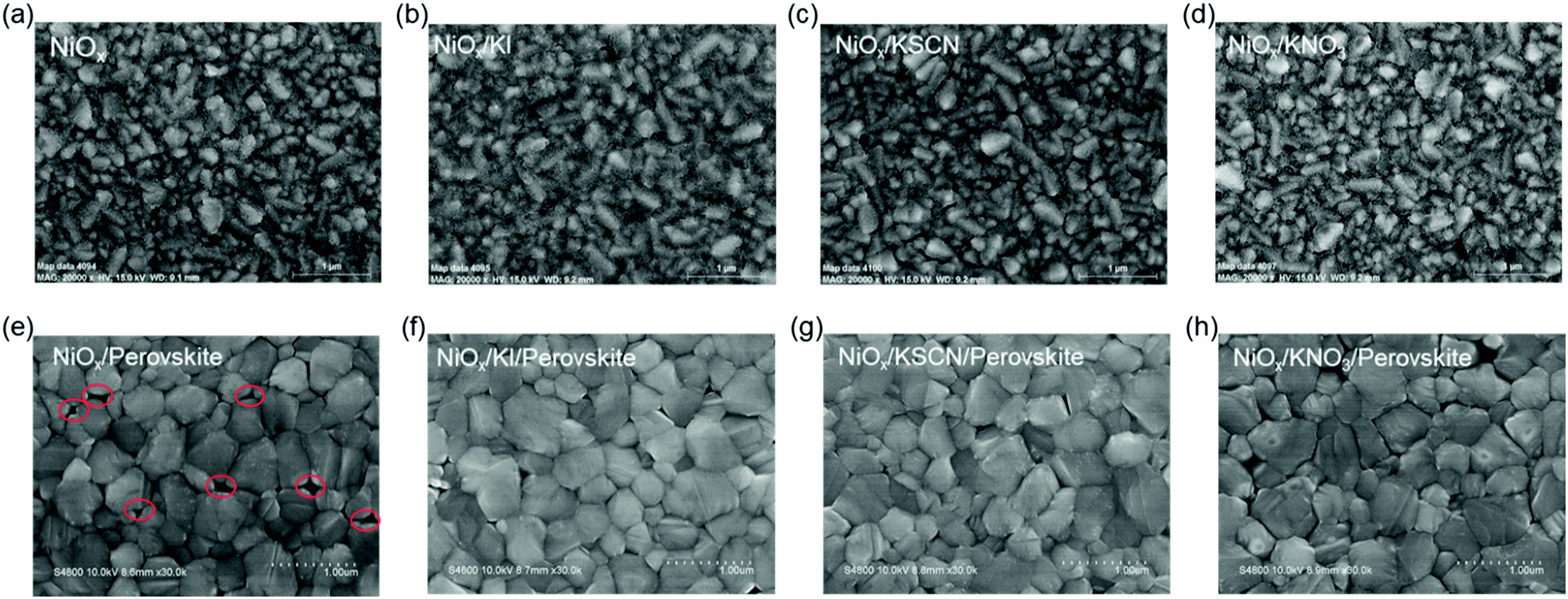 | ||
| Fig. 1 SEM images of (a) NiOX HTLs and (b) KI, (c) KSCN and (d) KNO3 modified NiOX HTLs. SEM images of perovskite layers grown on (e) NiOX HTL, (f) NiOX/KI HTL, (g) NiOX/KSCN HTL and (h) NiOX/KNO3 HTL. | ||
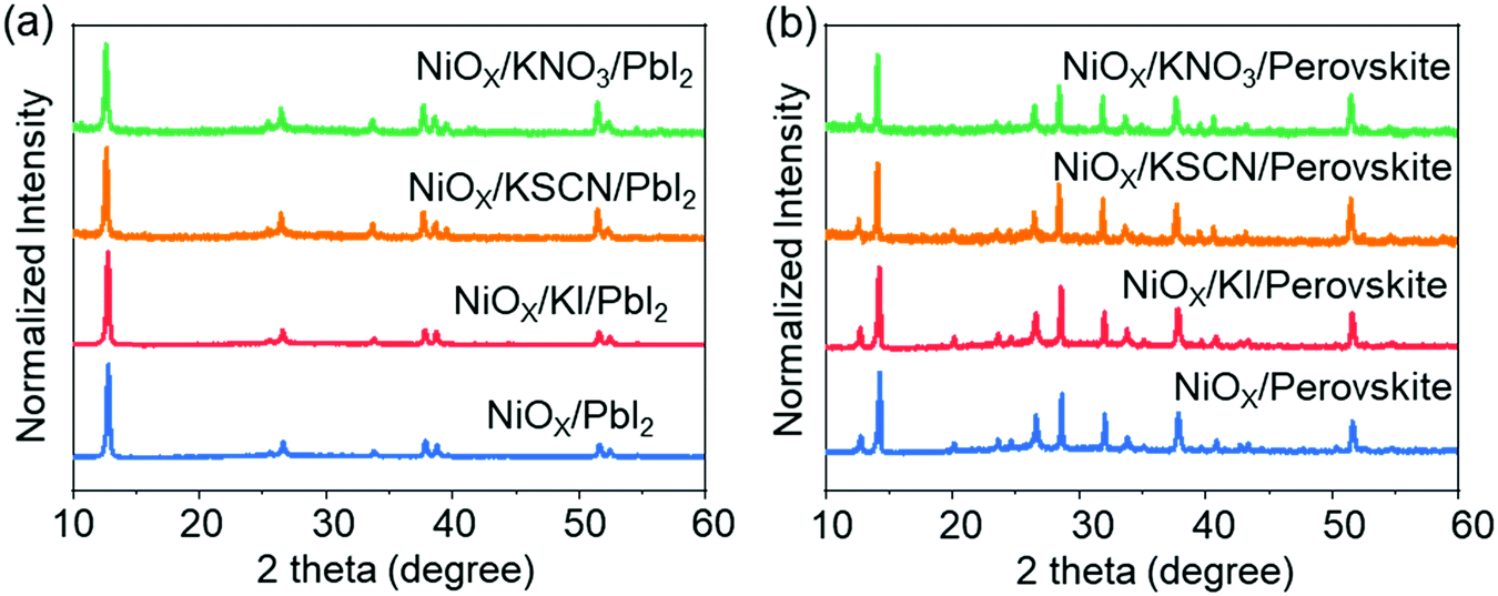 | ||
| Fig. 2 XRD patterns of (a) PbI2 and (b) perovskite thin films grown on the FTO/NiOX substrates with and without potassium salt modification. | ||
Inverted PSCs were fabricated to investigate the influence of potassium salts on photovoltaic performance. The device structure is fluorine-doped tin oxide (FTO)/NiOX/CH3NH3PbI3(MAPbI3)/[6,6]-phenyl-C61-butyric acid methyl ester (PCBM)/bathocuproine (BCP)/Ag (Fig. 3a). Current density–voltage (J–V) curves of PSCs with different HTLs are represented in Fig. 3b measured under standard air mass 1.5 global (AM 1.5G) illumination with a reverse scan rate of 0.15 V s−1. These detailed performance parameters are summarized in Table 1. The device treated by KI attained the highest PCE of 20.10% with a photocurrent density (JSC) of 22.81 mA cm−2, an open circuit voltage (VOC) of 1085 mV and a FF of 0.812. The stabilized power output of the champion device yielded a stabilized PCE of 20.03% after 200 s at maximum power point (MPP) under a bias of 0.9 V (Fig. 3c). And Fig. S3 (ESI†) displays the photocurrent density as a function of time for the best PSCs based on different NiOX HTLs held at a forward bias of MPP. Meanwhile, the external quantum efficiency (EQE) spectra of the KI modified devices also match well with the corresponding J–V measurements (Fig. 3d). Examples of J–V curves recorded at a scanning rate of 0.15 V s−1 are shown in Fig. 3e, where the reverse and forward scanning directions yielded PCE values of 20.10% and 19.70% for KI treated devices with little hysteresis. In the same batch, the devices based on NiOX/KSCN and NiOX/KNO3 HTL also revealed superior performances. The KSCN treated and KNO3 treated devices gave a PCE of 19.36% with a JSC of 22.95 mA cm−2, a VOC of 1050 mV and an FF of 0.803, and a PCE of 18.56% with a JSC of 22.81 mA cm−2, a VOC of 1075 mV and an FF of 0.757, respectively. By contrast, the pristine sample exhibited a JSC of 22.82 mA cm−2, VOC of 1064 mV and an FF of 0.752, and yielded a PCE of 18.25%. These devices by using modified NiOX HTLs also exhibit good stability, as shown in Fig. S4 (ESI†). To confirm the reproducibility of the devices, 48 individual cells based on KI, KSCN and KNO3 modification were measured to have a PCE of 18.81% ± 6.4%, 18.12% ± 5.7% and 18.00% ± 3.2%, respectively, all higher than 17.29 ± 5.4% of the pristine devices (Fig. 3f).
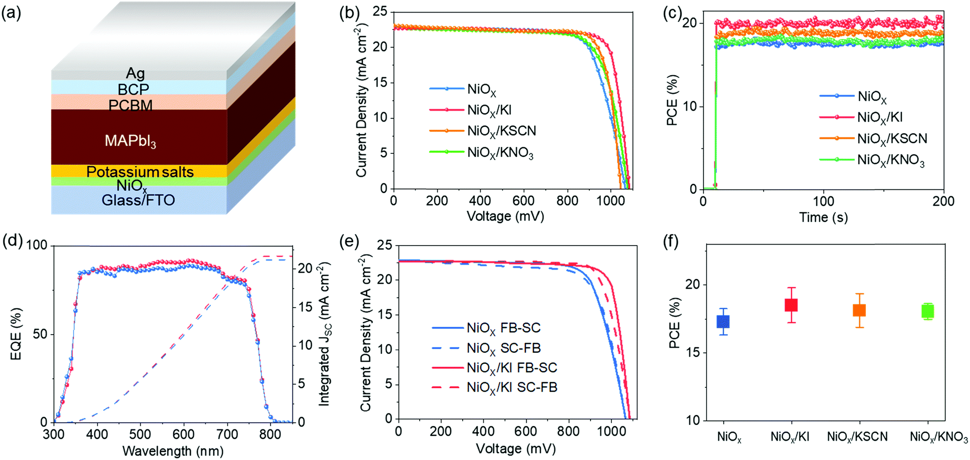 | ||
| Fig. 3 (a) Device architecture of PSCs. (b) J–V curves of PSCs based on NiOX, NiOX/KI, NiOX/KSCN and NiOX/KNO3 HTLs. (c) Steady-state power output of the device with and without modification measured at a fixed maximum power point (MPP) voltage as a function of time. (d) EQE spectra and the corresponding integrated photocurrent of the pristine (blue) and KI treated (red) device. (e) FB–SC and SC–FB J–V curves of KI treated and pristine champion devices measured with a scan rate of 0.15 V s−1. (f) Statistical photovoltaic parameters of PCE for devices based on different HTLs. | ||
| J SC (mA cm−2) | V OC (mV) | FF | PCE (%) | ||
|---|---|---|---|---|---|
| NiOX | Highest | 22.82 | 1064 | 0.752 | 18.25 |
| Average | 22.43 | 1058 | 0.732 | 17.29 | |
| NiOX/KI | Highest | 22.81 | 1085 | 0.812 | 20.10 |
| Average | 22.51 | 1077 | 0.772 | 18.81 | |
| NiOX/KSCN | Highest | 22.95 | 1050 | 0.803 | 19.36 |
| Average | 22.72 | 1046 | 0.762 | 18.12 | |
| NiOX/KNO3 | Highest | 22.81 | 1075 | 0.757 | 18.56 |
| Average | 22.18 | 1073 | 0.756 | 18.00 |
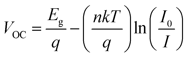
In addition, we further performed a detailed comparison between the PSCs based on NiOX and NiOX/potassium salt HTLs. We investigated the surface electronic properties of the pristine NiOx film and NiOX/KI films by ultraviolet photoelectron spectroscopy (UPS) and the results are exhibited in Fig. S5 (ESI†). The valence band positions versus vacuum level could be calculated to be 5.29 eV and 5.37 eV for the pristine NiOX and KI modified NiOX. In principle, deeper valence band maximum (VBM) of the HTLs close to the VBM of perovskite can result in better energy level alignment between the HTL and perovskite, which is beneficial for hole extraction and reducing the loss of photocarriers accumulated at the interface. The ideality factor (n) was measured to evaluate the recombination behavior of the PSCs. The ideality factor (n) of the devices can be inferred from the slope of VOC as a function of light intensity (I), according to the following equation:41
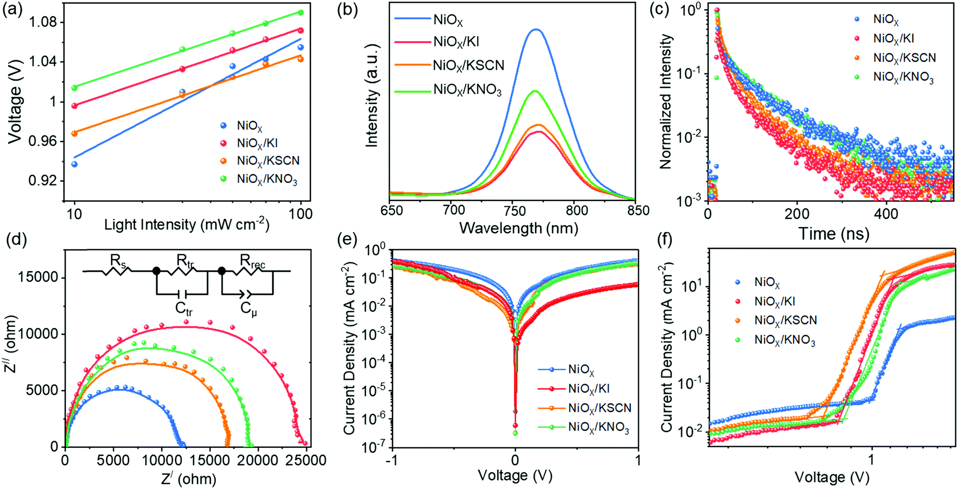 | ||
| Fig. 4 (a) Plots of light intensity dependent VOC of the pristine and potassium salt treated device. (b) Steady-state PL spectra and (c) TRPL spectra of perovskite films deposited on different NiOX substrates. (d) Nyquist plots recorded of PSCs based on pristine (blue) and KI (red), KSCN (orange), KNO3 (green) modified NiOX films with a frequency range of 1 MHz–100 Hz in 0.8 V. (e) Dark J–V curves of devices with and without modification. (f) SCLC curves of hole only devices deposited on different HTLs. | ||
Experimental
Substrate treatments
The patterned FTO-coated glass substrates were cleaned by ultrasonication with detergent, acetone, ethanol and deionized water in sequence for 20 min, then dried at 80 °C and finally treated with ultraviolet ozone cleaner for 15 min.Preparation of solution-derived NiOX films
Precursor solutions were prepared by dissolving 0.029 g nickel(II) 2-ethylhexanoate (78% w/w in 2-ethylhexanoic acid, Aldrich) in n-hexane (0.2436 g). The solutions were then spin-coated onto FTO at 4000 rpm for 60 s, followed by heated at 100 °C for 30 min; after cooling to room temperature, the film was calcined at 400 °C for 1 h.43Interfacial modification of NiOX film
KI, KSCN and KNO3 were dissolved in acetonitrile, respectively, with a molar concentration of 0.0525 M. Then the NiOX film was spin-coated at 4000 rpm for 60 s, followed by a heat treatment at 60 °C for 10 min.Synthesis of methylammonium iodide (CH3NH3I)
The CH3NH3I was prepared according to a reported method.44Device fabrication
PbI2 (1.30 M) (DMSO) complex solution in DMF was prepared by mixing 0.5993 g PbI2 (99.9985%, Alfa Aesar), 92 μL dimethyl sulfoxide (DMSO, 99.9%, Sigma-Aldrich) and 1 mL N,N-dimethylformamide (DMF, 99.9%, Alfa Aesar) with stirring at room temperature, overnight. The PbI2 (DMSO) solution was spin-coated on NiOX films with or without modification at 3000 rpm for 30 s, and then MAI solution (60 mg mL−1 in 2-propanol) was spin-coated on the top of the transparent PbI2 (DMSO) film at 5000 rpm for 30 s after loading for 5 s. The films changed to dark brown during spin coating and the films were dried on a hot plate at 100 °C for 10 min. Then, the PCBM (dissolved in chlorobenzene of 20 mg mL−1) and BCP (0.5 mg mL−1 in ethanol) were deposited by spin coating at 2000 rpm for 45 s, and 4000 rpm for 45 s. Finally, 110 nm Ag was thermally evaporated as the back electrode on the HTL.Characterization
The morphology and structure of the NiOX films were characterized by field emission scanning electron microscopy (FESEM, HITACHI S4800). The roughness and phase uniformity of the perovskite films were investigated by atomic force microscopy (AFM, Veeco/DI). The XRD spectra of the prepared powder were measured using powder X-ray diffraction (PXRD, Bruker D8 Advanced Diffractometer, Cu Kα radiation, 40 kV). The absorption spectra of the perovskite and the transmittance spectra of NiOX films were measured by using a Cary 500 UV-Vis-NIR spectrophotometer. The photoluminescence measurement was acquired at room temperature with a UV-Vis-NIR fluorescence spectrophotometer (Fluorolog-3-P) with an excitation wavelength of 515 nm. Electrochemical impedance spectroscopy (EIS) was carried out on an electrochemical workstation (Parstat 2273, Princeton) in the frequency range between 1 MHz and 100 Hz under short circuit at a forward bias of 0.2 V. The solar cells were illuminated using a solar light simulator (Solar IV-150A, Zolix) and the power of the simulated light was calibrated to 100 mW cm−2 using a newport calibrated KG5-filtered Si reference cell. J–V curves of solar cells were measured with a scan rate of 0.15 V s−1 under standard AM 1.5G irradiation of 100 mW cm−2 using a Keithley 2400 digital sourcemeter. Devices were masked with a metal aperture to define the active area of 0.0625 cm2. The stead state current output of the best-performing devices was measured by biasing the device at maximum power point for 200 s. The work function of the NiOX films was measured by UPS with a He source of incident energy 21.21 eV (He l line).Conclusions
In this research, we report a simple potassium salt modification strategy of NiOX based HTLs for inverted PSCs. This strategy can effectively increase the charge extraction capability of NiOX films and improve the perovskite films’ quality, leading to improved device performance. The champion device modified via KI attained a PCE of 20.10% with a JSC of 22.81 mA cm−2, a VOC of 1085 mV and an FF of 0.812, compared to 18.25% of the pristine sample. Our work indicates that potassium salt modified nickel oxides are excellent candidates to obtain high performance inverted PSCs and provides a simple and efficient approach for practical applications.Author contributions
X. L. and Y. H. designed the study. H. G. Y., S. Y. and Y. H. directed the study. X. L. performed the main experimental work. X. L., Q. H. W. and M. C. contributed to the characterizations. Y. H., B. G. and H. W. Q. analyzed the data. X. L., Y. H. and S. Y. wrote the manuscript. All authors revised the paper.Conflicts of interest
There are no conflicts to declare.Acknowledgements
This work was financially supported by the National Ten Thousand Talent Program for Young Top-notch Talent, the National Natural Science Fund for Distinguished Young Scholars (51725201), the National Natural Science Fund for Excellent Young Scholars (52022030), the National Natural Science Foundation of China (51972111 and 51902185), International (Regional) Cooperation and Exchange Projects of the National Natural Science Foundation of China (51920105003), Innovation Program of Shanghai Municipal Education Commission (E00014), the Fundamental Research Funds for the Central Universities (JKD012016025, JKD012016022), and Shanghai Engineering Research Center of Hierarchical Nanomaterials (18DZ2252400). The authors also thank the Frontiers Science Center for Materiobiology and Dynamic Chemistry.Notes and references
- K. Lin, J. Xing, L. N. Quan, F. P. G. De Arquer, X. Gong, J. Lu, L. Xie, W. Zhao, D. Zhang, C. Yan, W. Li, X. Liu, Y. Lu, J. Kirman, E. H. Sargent, Q. Xiong and Z. Wei, Perovskite light-emitting diodes with external quantum efficiency exceeding 20 per cent, Nature, 2018, 562(7726), 245–248 CrossRef CAS.
- T. Fang, T. Wang, X. Li, Y. Dong, S. Bai and J. Song, Perovskite QLED with an external quantum efficiency of over 21% by modulating electronic transport, Sci. Bull., 2021, 66(1), 36–43 CrossRef.
- T. Zhang, F. Wang, P. Zhang, Y. Wang, H. Chen, J. Li, J. Wu, L. Chen, Z. D. Chen and S. Li, Low-temperature processed inorganic perovskites for flexible detectors with a broadband photoresponse, Nanoscale, 2019, 11(6), 2871–2877 RSC.
- J. Song, T. Fang, J. Li, L. Xu, F. Zhang, B. Han, Q. Shan and H. Zeng, Organic-inorganic hybrid passivation enables perovskite QLEDs with an EQE of 16.48%, Adv. Mater., 2018, 30(50), 1805409 CrossRef.
- S. Yang, J. Dai, Z. Yu, Y. Shao, Y. Zhou, X. Xiao, X. C. Zeng and J. Huang, Tailoring passivation molecular structures for extremely small open-circuit voltage loss in perovskite solar cells, J. Am. Chem. Soc., 2019, 141(14), 5781–5787 CrossRef CAS.
- Y. Wang, M. I. Dar, L. K. Ono, T. Zhang, M. Kan, Y. Li, L. Zhang, X. Wang, Y. Yang, X. Gao, Y. Qi, M. Grätzel and Y. Zhao, Thermodynamically stabilized β-CsPbI3-based perovskite solar cells with efficiencies >18%, Science, 2019, 365(6453), 591–595 CrossRef CAS.
- A. Kojima, K. Teshima, Y. Shirai and T. Miyasaka, Organometal halide perovskites as visible-light sensitizers for photovoltaic cells, J. Am. Chem. Soc., 2009, 131(17), 6050–6051 CrossRef CAS.
- https://www.nrel.gov/pv/assets/pdfs/best-research-cell-efficiencies.20201217.pdf .
- A. K. Jena, A. Kulkarni and T. Miyasaka, Halide perovskite photovoltaics: background, status, and future prospects, Chem. Rev., 2019, 119(5), 3036–3103 CrossRef CAS.
- Z. Yang, A. Rajagopal and A. K.-Y. Jen, Organic-inorganic hybrid perovskite solar cells, Adv. Mater., 2017, 29(47), 1704418 CrossRef.
- L. Xie, P. Song, L. Shen, J. Lu, K. Liu, K. Lin, W. Feng, C. Tian and Z. Wei, Revealing the compositional effect on the intrinsic long-term stability of perovskite solar cells, J. Mater. Chem. A, 2020, 8(16), 7653–7658 RSC.
- J. Chen, D. J. Morrow, Y. Fu, W. Zheng, Y. Zhao, L. Dang, M. J. Stolt, D. D. Kohler, X. Wang, K. J. Czech, M. P. Hautzinger, S. Shen, L. Guo, A. Pan, J. C. Wright and S. Jin, Single-crystal thin films of cesium lead bromide perovskite epitaxially grown on metal oxide perovskite (SrTiO3), J. Am. Chem. Soc., 2017, 139(38), 13525–13532 CrossRef CAS.
- Z. Zhou, S. Yang, K. Xu, H. W. Qiao, J. Xie, Z. Lin, B. Ge, J. He, M. Chen, J. Zhang, Y. Hou and H. G. Yang, Diammonium-cesium lead halide perovskite with phase-segregated interpenetrating morphology for photovoltaics, J. Phys. Chem. Lett., 2020, 11(3), 747–754 CrossRef CAS.
- W. Yan, S. Ye, Y. Li, W. Sun, H. Rao, Z. Liu, Z. Bian and C. Huang, Hole-transporting materials in inverted planar perovskite solar cells, Adv. Energy Mater., 2016, 6(17), 1600474 CrossRef.
- W. Chen, Y. Zhou, G. Chen, Y. Wu, B. Tu, F. Z. Liu, L. Huang, A. M. C. Ng, A. B. Djurišić and Z. He, Alkali chlorides for the suppression of the interfacial recombination in inverted planar perovskite solar cells, Adv. Energy Mater., 2019, 9(19), 1803872 CrossRef.
- S. Pitchaiya, M. Natarajan, A. Santhanam, V. Asokan, A. Yuvapragasam, V. Madurai Ramakrishnan, S. E. Palanisamy, S. Sundaram and D. Velauthapillai, A review on the classification of organic/inorganic/carbonaceous hole transporting materials for perovskite solar cell application, Arabian J. Chem., 2020, 13(1), 2526–2557 CrossRef CAS.
- D. Ma, Y. Shen, T. Su, J. Zhao, N. U. Rahman, Z. Xie, F. Shi, S. Zheng, Y. Zhang and Z. Chi, Performance enhancement in up-conversion nanoparticle-embedded perovskite solar cells by harvesting near-infrared sunlight, Mater. Chem. Front., 2019, 3(10), 2058–2065 RSC.
- H. W. Qiao, S. Yang, Y. Wang, X. Chen, T. Y. Wen, L. J. Tang, Q. Cheng, Y. Hou, H. Zhao and H. G. Yang, A gradient heterostructure based on tolerance factor in high-performance perovskite solar cells with 0.84 fill factor, Adv. Mater., 2019, 31(5), 1804217 CrossRef.
- L. Xie, K. Lin, J. Lu, W. Feng, P. Song, C. Yan, K. Liu, L. Shen, C. Tian and Z. Wei, Efficient and stable low-bandgap perovskite solar cells enabled by a CsPbBr3-cluster assisted bottom-up crystallization approach, J. Am. Chem. Soc., 2019, 141(51), 20537–20546 CrossRef CAS.
- S. Wang, Y. Hua, M. Wang, F. Liu and L. Ding, CsPbI2.69Br0.31 solar cells from low-temperature fabrication, Mater. Chem. Front., 2019, 3(6), 1139–1142 RSC.
- J. You, L. Meng, T.-B. Song, T.-F. Guo, Y. Yang, W.-H. Chang, Z. Hong, H. Chen, H. Zhou, Q. Chen, Y. Liu, N. De Marco and Y. Yang, Improved air stability of perovskite solar cells via solution-processed metal oxide transport layers, Nat. Nanotechnol., 2015, 11(1), 75–81 CrossRef.
- J. X. Zhong, J. F. Liao, Y. Jiang, L. Wang, D. B. Kuang and W. Q. Wu, Synchronous surface and bulk composition management for red-shifted light absorption and suppressed interfacial recombination in perovskite solar cells, J. Mater. Chem. A, 2020, 8(19), 9743–9752 RSC.
- Y. Chen, Z. Yang, X. Jia, Y. Wu, N. Yuan, J. Ding, W. H. Zhang and S. Liu, Thermally stable methylammonium-free inverted perovskite solar cells with Zn2+ doped CuGaO2 as efficient mesoporous hole-transporting layer, Nano Energy, 2019, 61, 148–157 CrossRef CAS.
- B. Ge, H. W. Qiao, Z. Q. Lin, Z. R. Zhou, A. P. Chen, S. Yang, Y. Hou and H. G. Yang, Deepening the valence band edges of NiOX contacts by alkaline earth metal doping for efficient perovskite photovoltaics with high open-circuit voltage, Sol. RRL, 2019, 3(8), 1900192 CrossRef.
- W. Chen, Y. Wu, J. Fan, A. B. Djurišić, F. Liu, H. W. Tam, A. Ng, C. Surya, W. K. Chan, D. Wang and Z.-B. He, Understanding the doping effect on NiO: toward high-performance inverted perovskite solar cells, Adv. Energy Mater., 2018, 8(19), 1703519 CrossRef.
- L. Xu, X. F. Chen, J. J. Jin, W. Liu, B. Dong, X. Bai, H. W. Song and P. Reiss, Inverted perovskite solar cells employing doped NiO hole transport layers: a review, Nano Energy, 2019, 63, 103860 CrossRef CAS.
- J. Tian, Q. Xue, X. Tang, Y. Chen, N. Li, Z. Hu, T. Shi, X. Wang, F. Huang, C. J. Brabec, H. L. Yip and Y. Cao, Dual interfacial design for efficient CsPbI2Br perovskite solar cells with improved photostability, Adv. Mater., 2019, 31(23), 1901152 CrossRef.
- Y. Bai, H. Chen, S. Xiao, Q. Xue, T. Zhang, Z. Zhu, Q. Li, C. Hu, Y. Yang, Z. Hu, F. Huang, K. S. Wong, H. L. Yip and S. Yang, Effects of a molecular monolayer modification of NiO nanocrystal layer surfaces on perovskite crystallization and interface contact toward faster hole extraction and higher photovoltaic performance, Adv. Funct. Mater., 2016, 26(17), 2950–2958 CrossRef CAS.
- P. Schulz, D. Cahen and A. Kahn, A halide perovskites: is it all about the interfaces?, Chem. Rev., 2019, 119(5), 3349–3417 CrossRef CAS.
- I. Zarazua, G. Han, P. P. Boix, S. Mhaisalkar, F. Fabregat-Santiago, I. Mora-Sero, J. Bisquert and G. Garcia-Belmonte, Surface recombination and collection efficiency in perovskite solar cells from impedance analysis, J. Phys. Chem. Lett., 2016, 7(24), 5105–5113 CrossRef CAS.
- D. J. Kubicki, D. Prochowicz, A. Hofstetter, S. M. Zakeeruddin, M. Grätzel and L. Emsley, Phase segregation in potassium-doped lead halide perovskites from 39K solid-state NMR at 21.1 T, J. Am. Chem. Soc., 2018, 140(23), 7232–7238 CrossRef CAS.
- J. K. Nam, S. U. Chai, W. Cha, Y. J. Choi, W. Kim, M. S. Jung, J. Kwon, D. Kim and J. H. Park, Potassium incorporation for enhanced performance and stability of fully inorganic cesium lead halide perovskite solar cells, Nano Lett., 2017, 17(3), 2028–2033 CrossRef CAS.
- X. Liu, Y. Cheng, C. Liu, T. Zhang, N. Zhang, S. Zhang, J. Chen, Q. Xu, J. O. Yang and H. Gong, 20.7% highly reproducible inverted planar perovskite solar cells with enhanced fill factor and eliminated hysteresis, Energy Environ. Sci., 2019, 12(5), 1622–1633 RSC.
- P. Zhu, S. Gu, X. Luo, Y. Gao, S. Li, J. Zhu and H. Tan, Simultaneous contact and grain-boundary passivation in planar perovskite solar cells using SnO2-KCl composite electron transport layer, Adv. Energy Mater., 2020, 10(3), 1903083 CrossRef CAS.
- W. Chen, Y. Zhou, G. Chen, Y. Wu, B. Tu, F.-Z. Liu, L. Huang, A. M. C. Ng, A. B. Djurišić and Z. He, Alkali chlorides for the suppression of the interfacial recombination in inverted planar perovskite solar cells, Adv. Energy Mater., 2019, 9(19), 1803872 CrossRef.
- F. Zheng, W. Chen, T. Bu, K. P. Ghiggino, F. Huang, Y. Cheng, P. Tapping, T. W. Kee, B. Jia and X. Wen, Triggering the passivation effect of potassium doping in mixed-cation mixed-halide perovskite by light illumination, Adv. Energy Mater., 2019, 9(24), 1901016 CrossRef.
- J. Burschka, N. Pellet, S.-J. Moon, R. Humphry-Baker, P. Gao, M. K. Nazeeruddin and M. Grätzel, Sequential deposition as a route to high-performance perovskite-sensitized solar cells, Nature, 2013, 499(7458), 316–319 CrossRef CAS.
- J. Kim, Y. Lee, A. J. Yun, B. Gil and B. Park, Interfacial modification and defect passivation by the cross-linking interlayer for efficient and stable CuSCN-based perovskite solar cells, ACS Appl. Mater. Interfaces, 2019, 11(50), 46818–46824 CrossRef CAS.
- M. M. Byranvand, T. Kim, S. Song, G. Kang, S. U. Ryu and T. Park, p-Type CuI islands on TiO2 electron transport layer for a highly efficient planar-perovskite solar cell with negligible hysteresis, Adv. Energy Mater., 2018, 8(5), 1702235 CrossRef.
- S. You, H. Wang, S. Bi, J. Zhou, L. Qin, X. Qiu, Z. Zhao, Y. Xu, Y. Zhang, X. Shi, H. Zhou and Z. Tang, A biopolymer heparin sodium interlayer anchoring TiO2 and MAPbI3 enhances trap passivation and device stability in perovskite solar cells, Adv. Mater., 2018, 30(22), 1706924 CrossRef.
- J. He, J. Liu, Y. Hou, Y. Wang, S. Yang and H. G. Yang, Surface chelation of cesium halide perovskite by dithiocarbamate for efficient and stable solar cells, Nat. Commun., 2020, 11(1), 4237 CrossRef CAS.
- M. Jeong, I. W. Choi, E. M. Go, Y. Cho, M. Kim, B. Lee, S. Jeong, Y. Jo, H. W. Choi, J. Lee, J.-H. Bae, S. K. Kwak, D. S. Kim and C. Yang, Stable perovskite solar cells with efficiency exceeding 24.8% and 0.3 V voltage loss, Science, 2020, 369(6511), 1615–1620 CAS.
- L. J. Tang, X. Chen, T. Y. Wen, S. Yang, J. J. Zhao, H. W. Qiao, Y. Hou and H. G. Yang, A solution-processed transparent NiO hole-extraction layer for high-performance inverted perovskite solar cells, Chem. – Eur. J., 2018, 24(12), 2845–2849 CrossRef CAS.
- Y. Hou, X. Chen, S. Yang, Y. L. Zhong, C. Li, H. Zhao and H. G. Yang, Low-temperature processed In2S3 electron transport layer for efficient hybrid perovskite solar cells, Nano Energy, 2017, 36, 102–109 CrossRef CAS.
Footnote |
| † Electronic supplementary information (ESI) available. See DOI: 10.1039/d0qm01064b |
| This journal is © the Partner Organisations 2021 |