 Open Access Article
 This Open Access Article is licensed under a Creative Commons Attribution-Non Commercial 3.0 Unported Licence
Optoelectronic conversion and polarization hysteresis in organic MISM and MISIM devices with DA-type single-component molecules†
Akihiro
Tomimatsu
a,
Rie
Suizu
 ab,
Miyabi
Nakazawa
c,
Takashi
Shirahata
cd,
Yohji
Misaki
cd,
Naoya
Kinoshita
a and
Kunio
Awaga
*a
ab,
Miyabi
Nakazawa
c,
Takashi
Shirahata
cd,
Yohji
Misaki
cd,
Naoya
Kinoshita
a and
Kunio
Awaga
*a
aDepartment of Chemistry & Integrated Research Consortium on Chemical Sciences (IRCCS), Nagoya University, Furo-cho, Chikusa-ku, Nagoya 464-8602, Japan. E-mail: awaga.kunio.h8@f.mail.nagoya-u.ac.jp
bJapan Science and Technology Agency (JST), PRESTO, 4-1-8 Honcho, Kawaguchi, Saitama 332-0012, Japan
cDepartment of Applied Chemistry, Graduate School of Science and Engineering, Ehime University, Matsuyama, 790-8577, Japan
dResearch Unit for Materials Development for Efficient Utilization and Storage of Energy, Ehime University, 790-8577, Japan
First published on 4th September 2023
Abstract
Organic electronic devices offer various advantages, such as low cost and tunability. However, the organic semiconductors used in these devices have significant drawbacks, including instability in air and low carrier mobility. To address these challenges, we recently introduced organic MISM and MISIM (M = metal, I = insulator, S = semiconductor) devices, which effectively generate photo-induced displacement current and exhibit ferroelectric behavior. In previous studies, the S layer consisted of an organic donor–acceptor (DA) bilayer. In the present research, we fabricated MISM and MISIM devices using DA-type single-component molecules as the S layer and examined their photocurrent and polarization hysteresis. While the performance of these devices does not surpass that of DA bilayer devices, we discovered that DA-type single-component molecules can be utilized for photoelectric conversion and polarization trapping.
Introduction
Organic optoelectronic conversion has attracted much attention from both scientific and industrial communities due to its advantages over traditional inorganic counterparts. For example, organic electronic devices can be intrinsically lightweight and mechanically flexible because organic semiconductors are loosely packed due to van der Waals interactions. In addition, their performance is tuneable, because the physical and chemical properties of organic semiconductors are easily tailored by chemical modification. For these reasons, organic photovoltaic (OPV) cells are considered not only as a new environmentally friendly and sustainable energy source to replace existing fossil fuels, but also as a candidate to meet the modern demand for a compact and portable energy source as information technology develops toward the Internet of Things.1,2 Indeed, OPVs are expected to be used in applications such as wearable devices,3 indoor light-harvesting systems,4–6 and semitransparent solar cells integrated in the windows of buildings.7 However, even though recent organic field-effect transistors (OFETs) have achieved high carrier mobilities of more than 10 cm2 V−1 s−1,8–10 the carrier mobilities of organic semiconductors are usually much lower than those of inorganic semiconductors.11,12 In addition, organic photocells lack stability because oxidation by oxygen and water in the atmosphere and photochemical reactions caused by UV radiation from sunlight result in the degradation of the active layers.13,14 While it is important to develop materials to solve these problems, it is especially desirable to develop new operating principles for organic optoelectronic conversions.While early-stage research on organic optoelectronic conversion focused on the Schottky junction, which is formed between an organic semiconductor layer and a metal electrode,15 Tang reported in 1985 the first OPV with a donor–acceptor (DA) heterojunction using copper phthalocyanine (CuPc) as a donor and 3,4,9,10-perylenetetracarboxylic bisbenzimidazole (PTCBI) as an acceptor.16 This was followed by the extensive pursuit of a way to improve the performance of OPVs by developing organic DA materials, including polymers, and studying the structures of DA interfaces, such as bulk heterojunctions. Recently, we proposed a [metal (M)|organic insulator (I)|organic semiconductor (S)|metal (M)] (MISM, see Scheme 1) structure that can be applied as an organic differential photoelectric conversion device for information conversion and as an alternating current (AC)-type OPV.17,18 The MISM photocell can be regarded as a photocapacitor, in which charge separation occurs in the S layer upon light irradiation and the generated carriers create a transient photocurrent in the external circuit (ION), inducing polarization in the I layer. In other words, photon energy is stored in the I layer as electrical polarization. An important feature of this MISM photocell is that the polarization of the I layer synergistically promotes charge separation in the S layer, enhancing ION. When the light is turned off, the polarization of the I layer is released and a reverse current is generated in the external circuit (IOFF). Another important feature of MISM photocells is that large polarization is more important than high mobility for improving performance, since the displacement current causes photoelectric conversion in MISM photocells. Although MISM photocells cannot generate direct current (DC) under constant light irradiation, they can effectively convert modulated light into AC through a mechanism that is gentle to organic materials.
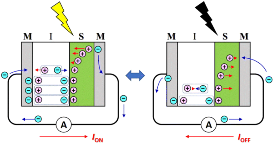 | ||
| Scheme 1 Operating mechanism of the MISM photocell. During light irradiation, charge separation occurs in the S layer, and the resulting carriers induce polarization in the I layer. This polarization synergistically enhances charge separation in the S layer, leading to a significant transient photocurrent in the external circuit (ION). During light-off, depolarization takes place in the I layer, causing a reverse current to appear in the external circuit (IOFF). | ||
The performance of MISM photocells depends not only on the materials used for the S layer but also on those used for the I layer. High responsivity can be obtained by an insulator with a high dielectric constant, while high bandwidth can be obtained by an insulator with a low dielectric constant.19,20 In fact, we have discovered that the AC of MISM photovoltaic cells can be greatly enhanced by utilizing an electrolyte, such as an ionic liquid, as the I-layer.19 Moreover, by capitalizing on the fact that the formation of the electric double layer at the M|I interface is nearly unaffected by the thickness of the I layer, we have developed an on-plate photodetector where all components are positioned on a single plate,21 in contrast to the sandwich structure commonly found in organic photocells.
We have also proposed MISIM photocells (see Scheme 2) to generate transient current in response to light irradiation and blocking, similar to MISM photocells.22 The mechanism in MISIM photocells is nearly identical to that in MISM photocells. However, in MISM photocells, a portion of the charge carriers generated in the S layer is extracted from the electrode, whereas in MISIM photocells, all generated charge carriers accumulate at the I|S interface. This accumulation leads to current oscillations induced in the external circuit through polarization/depolarization in the I layers. Since the S layer is completely isolated from the metal electrodes by the I layers, there should be no carrier transfer between the S layer and those electrodes. Additionally, it has been discovered that MISIM photocells can simultaneously achieve high responsivity and high bandwidth by combining high- and low-capacitance insulators for the two I layers.22
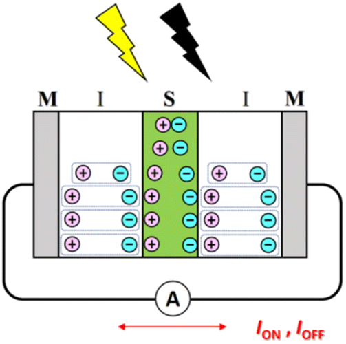 | ||
| Scheme 2 Operating mechanism of the MISIM photocell. Light irradiation induces synergetic polarizations in the S and I layers, while blocking leads to their depolarization, leading to AC in the external circuit. | ||
We have also demonstrated that the organic MISIM structure exhibits hysteresis loops in the polarization–voltage (P–V) curves without the use of ferroelectric materials.23Scheme 3 depicts a model of this device, where the S layer comprises positive and negative elementary charges, namely +ve and −ve, which are induced by an electric field. The I layers are considered to be induced dipoles, caused separately by +ve and −ve. In Scheme 3a, U(r) and U′(r) represent the electrostatic potentials between the positive and negative charges in the S layer and between the positive/negative charge and the induced dipole in the I layer. We calculated the total potential, denoted as Utotal(r) = U(r) + 2U′(r), using realistic values for the device length (R = 200 nm), the polarizability of the I layer (α = 10 × 10−40 J−1 C2 m2), and the dielectric constants of the S layer (εr = 1, 3, 10, and 100). Scheme 3b illustrates Utotal(r), showing a potential barrier between the two minima. The arrow Δ in this scheme indicates the thermal energy at 300 K on the εr = 1 curve (blue curve). This suggests that once the positive and negative charges are separated by an external field to a distance of r < 0.5 nm (as indicated by the broken arrow in Scheme 3b), the potential barrier for charge recombination becomes larger than the thermal energy at 300 K. This model suggests that interfacial polarization is stabilized and that hysteresis is induced between the processes of polarization and depolarization.
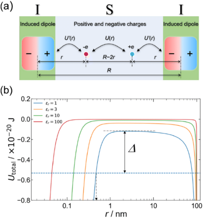 | ||
| Scheme 3 (a) Electrostatic model of the MISIM device, consisting of positive and negative charges in the S layer and induced dipoles in the I layers. U(r) and U′(r) indicate the electrostatic potentials between the positive and negative charges in the S layer and between the positive/negative charges and the induced dipole in the I layer. (b) Theoretical curves for the model in panel (a) with R = 200 nm and four assumed values for the dielectric constant of the S layer, namely εr = 1, 3, 10, and 100. The arrow Δ indicates the thermal energy of 300 K on the blue curve. | ||
In our previous studies of the MISM and MISIM devices, we employed organic DA bilayers as the S layer. This allowed us to achieve photoinduced charge separation and field-induced polarization in the S layer. In the present study, we investigated whether photoelectric conversion and ferroelectric hysteresis can be achieved from a simpler structure using DA-type single-component molecules as the S-layer.
Results and discussion
Electronic structures of ET-PRBT and EO-PRBT
The synthesis of ET-PRBT (ethylenedithio-pyrrolobenzothiazole-tetrathiafluvalene) and EO-PRBT (ethylenedioxy-pyrrolobenzothiazole-tetrathiafluvalene) (see the inset of Fig. 1) will be reported elsewhere. Their chemical identifications were performed by NMR, IR, structural analysis, etc.Fig. 1 shows the energy diagram for the HOMOs and LUMOs of the two molecules, calculated by density functional theory (DFT, B3LYP/6-31G(d,p)), as well as the work function of the electrodes, namely ITO and Ag. The HOMO energy of ET-PRBT is lower than that of EO-PRBT by 0.2 eV, while their LUMO levels are nearly the same. The HOMO levels of the two molecules are energetically close to the Fermi levels of the electrodes. This figure also shows the shapes of the HOMO and LUMO for ET-PRBT, which are nearly the same as those for EO-PRBT (not shown). It is characteristic of the two molecules that the HOMO and LUMO are rather localized on the thiafulvalene (donor) and thiazole (acceptor) moieties, respectively. This spatial separation of the HOMO and LUMO is expected to generate a significant dipole moment upon irradiation and in the presence of an electric field, leading to the generation of displacement current and exhibiting ferroelectric behaviour, respectively.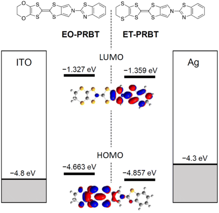 | ||
| Fig. 1 Energy diagram for the HOMOs and LUMOs of ET-PRBT and EO-PRBT, and for the work functions of ITO and Ag electrodes. | ||
Thin films (30 nm) of ET-PRBT and EO-PRBT were formed by vacuum sublimation on quartz substrates. Their XRD patterns are shown in Fig. S1† and indicate good crystallinity. However, there was no exact correspondence with the single-crystal X-ray data, indicating a notable disparity between them. Fig. 2 compares the UV-vis absorption spectra of the THF solution samples and thin films for ET-PRBT and EO-PRBT. The solution spectra exhibit strong absorption bands at 380 nm, which are attributed to the HOMO–LUMO transitions that each possess an intramolecular charge transfer (CT) feature. In contrast, the thin films show broad and weak absorption bands at 520 nm. A preliminary crystal structure analysis of ET-PRBT suggests an intermolecular overlap between the D and A moieties, indicating that these bands are likely due to an intermolecular CT band between them.
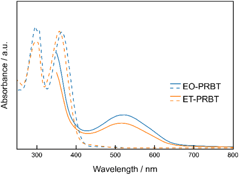 | ||
| Fig. 2 UV-vis absorption spectra of the THF solution samples (broken curves; 10−4 M) and thin films (solid curves; 30 nm) for ET-PRBT and EO-PRBT. | ||
MISM photocells
We first prepared the MISM photocells of ET-PRBT and EO-PRBT using ITO and Ag as the electrodes and parylene C (PC) as the I layer. The thicknesses of the S and I layers are 30 and 230 nm, respectively. We formed two types of photocells, [ITO|I|S|Ag] and [ITO|S|I|Ag], where the S layer consisted of either ET-PRBT or EO-PRBT. We then examined the photocurrent produced when the cells were illuminated with a green laser (λ = 532 nm) modulated by a mechanical chopper (1 kHz). Note that this illumination excited the weak bands of ET-PRBT and EO-PRBT at 520 nm. The results for the [ITO|I|S|Ag] cell are shown in Fig. 3a, where the gray broken curve is the response from a Si diode to monitor the light-on and -off periods. These photocells exhibit photo-induced alternating current (AC), with the peak current for ET-PRBT being approximately five times that of EO-PRBT. These photocurrents are believed to be caused by a Schottky barrier at the S|Ag interface. Fig. 3b displays the results for the [ITO|S|I|Ag] photocells, where the order of the S and I layers between ITO and Ag is reversed. These cells also demonstrate photo-induced AC, likely due to a Schottky barrier at the ITO|S interface. The peak current value for the [ITO|ET-PRBT|I|Ag] cell is nearly half that of the [ITO|I|ET-PRBT|Ag] cell, while those of the two EO-PRBT cells are nearly the same. However, the [ITO|I|S|Ag] and [ITO|S|I|Ag] cells differ in a crucial respect: their phases of the photo-induced AC are completely opposite in terms of the light-on and -off periods. Their phases can be explained by assuming that the photo-induced AC in these photocells is triggered by electron transfer from the S layer to the electrode directly facing the S layer.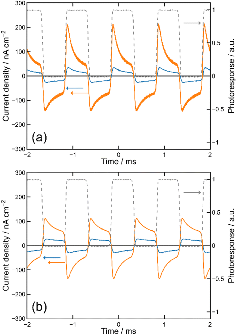 | ||
| Fig. 3 Time trajectory of the transient photocurrent for the [ITO|I|S|Ag] (a) and [ITO|S|I|Ag] (b) photocells. The orange and blue curves show the photocurrents when S = ET-PRBT and EO-PRBT, respectively, and the gray broken curves indicate the response from a Si diode to monitor the light-on and -off periods. | ||
MISIM photocells
We then formed MISIM photocells for ET-PRBT and EO-PRBT, with an S layer thickness of 30 nm and a PC I layer thickness of 230 nm. We examined the photocurrent of the MISIM photocells under the same experimental conditions used for the MISM photocells. The results are shown in Fig. 4. Although the observed photo-induced AC was one order of magnitude smaller than that in the MISM photocells, the MISIM photocells, which consist of S layers with single-component molecules, were found to produce AC. The AC in the ET-PRBT photocell is larger than that in the EO-PRBT photocell, as observed in the MISM photocells. The AC phases in the two MISIM photocells are the same and are consistent with that in the [ITO|I|S|Ag] (MISM) photocell, shown in Fig. 3a. This indicates that, during light-on, positive current flows from Ag to ITO in the external circuit. Since this cannot be explained by the potential difference between the electrodes, it is presumably caused by the S-layer molecular orientation formed in the device fabrication procedure.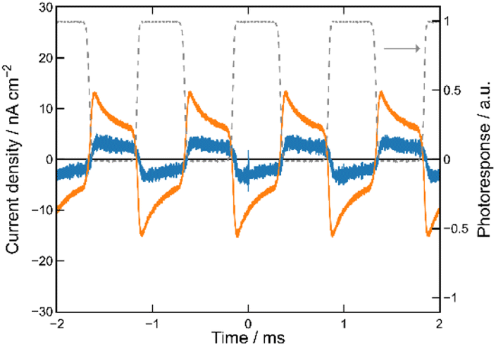 | ||
| Fig. 4 Time trajectory of the transient photocurrent for the [ITO|I|S|I|Ag] photocell. The orange and blue curves show the photocurrent when S = ET-PRBT and EO-PRBT, respectively, and the gray broken curve indicates the response from a Si diode to monitor the light-on and -off periods. | ||
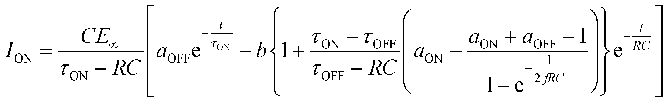
In our previous work,24 we developed theoretical equations to analyze the photocurrent of the MISIM cell. The circuit of the MISIM photocell becomes equivalent to that of the MISM cell by combining the two I layers in the MISIM cell under the condition that there is no current leakage through the I layers. Therefore, the MISIM photocell can be expressed by the simple circuit shown in the inset of Fig. 5, where E represents the voltage of the S layer, C and V are the combined capacitance and voltage of the I layers, respectively, I is the current flowing through the external circuit, and R represents effective resistance in the present photocell circuit. The time trajectories of the current during light-on and -off, namely ION and IOFF, can be written by the following equations, where f represents the modulation frequency (1 kHz) and E∞ corresponds to the open-circuit voltage of the S layer. Additionally, τON represents the time constant that determines how fast the polarization of the S layer reaches the open-circuit voltage, while τOFF represents the time constant that determines how fast the polarization of the S layer relaxes. Note that τON and τOFF are merely fitting parameters used to explain the time trajectory of the transient photocurrent.
 | (1) |
 | (2) |
 | (3) |
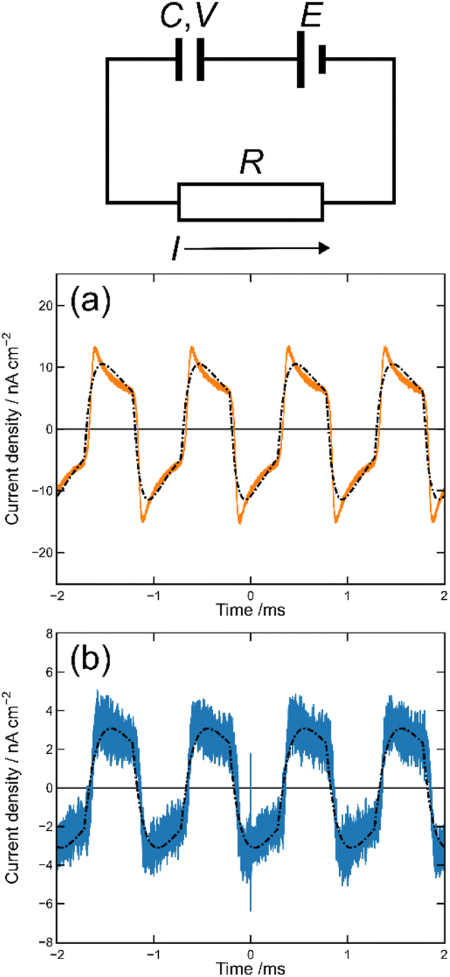 | ||
| Fig. 5 Results of the photocurrent analysis in the MISIM photocells with S = ET-PRBT (a) and S = EO-PRBT (b). The broken curves represent the theoretical best fits of eqn (1) and (2). The inset schematically shows the model circuit for the MISIM photocell, where E corresponds to the voltage of the S layer, C and V to the capacitance and voltage of the I layers, respectively, and I and R to the current flowing and the effective resistance, respectively. | ||
MISIM ferroelectric cells
A hallmark of ferroelectrics is the spontaneous electric polarization that can be reversed by applying an electric field, resulting in hysteresis loops in the P–V curves.25 Recently, molecular organic ferroelectrics have garnered significant attention due to their distinctive properties, including low environmental impact, light weight, and flexibility.26,27 While various ferroelectric molecular crystals have been developed, the production of ferroelectric molecular thin films remains limited, despite their importance in practical applications.28–30 This limitation is primarily attributed to a significant decrease in polarization and to the irreversibility of polarization. While conventional ferroelectric materials consist of microscopic polarizations that are periodically aligned throughout the entire crystal, such as D+A−D+A−D+A−⋯D+A−, ferroelectric behaviour can be achieved through interfacial polarization, such as D+A0D0A0D0A0⋯D0A−, which arises from the separation of positive and negative charges at the ends. If the interfacial polarization induced by an electric field is retained by certain trapping mechanisms of the surface charges, ferroelectric behaviour can be observed.31,32 It is worth noting that this interfacial mechanism is suitable for the development of thin film organic ferroelectrics.In the previous section, we described the MISIM photocells, where the electrical polarization in the I layer enhances the separation of photo-induced charges in the S layer and traps the photo-generated carriers at the I|S interfaces. We proposed an MISIM structure to stabilize the interfacial polarization.23 Specifically, as shown in Scheme 3, the interfacial polarization is induced in the S layer by an external electric field even in the absence of light. In this case, the polarizations present in the I layers play a crucial role in stabilizing the induced interfacial polarization within the S layer. Additionally, the insulation of the S layer by the I layers from the metal electrodes was expected to allow for the application of high voltage to this device, thereby enhancing the interfacial polarization in the S layer. We fabricated a MISIM device with S as a thin film of a CT complex, TMB-TCNQ (3,3′,5,5′-tetramethylbenzidine - tetracyanoquinodimethane), and I as PC. We demonstrated the presence of polarization hysteresis, exhibiting a large remnant polarization (Pr) of 0.2 μC cm−2 that remained stable over the wide temperature range of 80–320 K.23
In this study, we conducted P–V curve measurements for a MISIM device, specifically [ITO|PC|ET-PRBT|PC|Ag], at room temperature. The measurement method is described in the Experimental section below and Fig. S2.† The results of three scans are shown in Fig. 6, clearly indicating hysteresis loops in the P–V curves. The value of Pr was estimated to be ca. 0.02 μC cm−2, which is one order of magnitude smaller than that of the TMB-TCNQ MISIM device but comparable to those of the ZnPc and C60 MISIM devices.23 The value of the coercive voltage, Vc, is approximately 100 V, which is nearly identical to that of the TMB-TCNQ device.23 This suggests the presence of the same trapping mechanism for interface polarization.
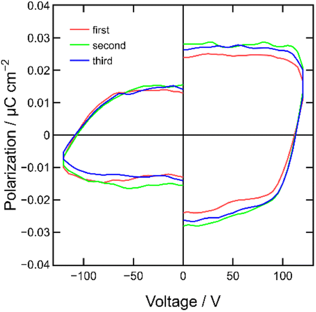 | ||
| Fig. 6 P–V hysteresis curves of the MISIM ([ITO|PC|ET-PRBT|PC|Ag]) device at room temperature. | ||
Discussion
We described the optoelectronic conversions of the MISM and MISIM photocells, in which the S layers were composed of single-component DA-type molecules, either ET-PRBT or EO-PRBT. These molecules successfully converted the modulated light to AC, but the photocurrent intensity was smaller than those of the previous photocells, in which the S layers were composed of bilayers of D and A molecules. This is likely caused by the fact that, although we excited the potential intermolecular CT bands at 520 nm, the absorption was weak due to the small absorbance of these bands. As a result, this excitation did not effectively induce charge separations. In other words, the performance of these photocells, similar to the previous DA bilayer photocells, was governed by the charge separation occurring within the S layers. In addition, the values of τON and τOFF for the ET-PRBT and EO-PRBT photocells are three orders of magnitude longer than that for the ZnPc/C60 bilayer photocell (see Table 1). For the ET-PRBT and EO-PRBT photocells, this indicates a slow transfer of carriers to the I|S interfaces when exposed to light, leading to polarization in the I layer, as well as to a delayed charge recombination process during light-off. These are likely caused by the absence of a D|A interface in the S layer, which would normally generate a potential gradient for the carriers, and by the high resistivity of carriers within the lattice of DA-type molecules.We also examined the P–V curves of the MISIM device with S = ET-PRBT. Although we clearly found hysteresis loops, the Pr value was one order of magnitude smaller than that of MISIM with S = TMB-TCNQ. It is likely that Pr of these devices is governed by the degree of intermolecular CT in ET-PRBT and TMB-TCNQ.
Experimental
Device fabrication
All devices used for the measurements were fabricated with indium tin oxide (ITO) as the transparent electrode, parylene C (PC) (230 nm) as the I layers, EO-PRBT or ET-PRBT (30 nm) as the S layer, and silver (Ag) as the top electrode. The present devices were fabricated as follows. The ITO patterned glass substrates, with 2 mm-wide stripes, were cleaned with aqueous 0.5 vol% Hellmanex III solution, acetone, and 2-propanol in that order for 15 min each by sonication, dried in an oven at 120 °C for 1 h, and treated with UV/O3 (Bioforce Nanosciences ProCleaner) for 30 min prior to use in the experiment. The EO-PRBT, ET-PRBT, and Ag layers were prepared by vacuum deposition at a base pressure of ≤3 × 10⁻⁴ Pa, and the deposition rates for EO-PRBT and ET-PRBT were 0.1–0.5 Å s−1, while that for Ag was 0.2–0.3 Å s−1. The thicknesses of the EO-PRBT and ET-PRBT layers were monitored using a quartz crystal microbalance during deposition and measured with white light interference microscopy (Nikon BW-S507), revealing thicknesses of about 30 nm for both EO-PRBT and ET-PRBT. The top Ag electrode was 2 mm wide and orthogonal to ITO, forming a 4 mm2 active area. PC was deposited by a Specialty Coating Systems PDS2010 deposition unit, and the thickness was about 230 nm, as measured by white light interference microscopy.Photocurrent measurements
A laser diode (λmax = 532 nm, CrystaLaser CL532-025-L) with a light intensity of about 5.1 mW cm−2 was used as a light source without any collimation. The light was then modulated by a light chopper (NF Corporation 5584A) and used to irradiate the photocells from the ITO side. The shape of the irradiated spot was elliptical, with major and minor axes of about 3 and 2 mm, respectively. The spot covered the active area of the photocell.The generated transient photocurrent was amplified with a transimpedance amplifier (Femto DHPCA-100) in low-noise mode, where its gain setting, bandwidth, and rise/fall time were 107 V A−1, 220 MHz, and 1.6 μs, respectively, and measured with an oscilloscope (Tektronix MSO54) in average mode. In data analysis, we assumed that the transient photocurrent came from the active area because the contribution from other irradiated parts was considered negligible.33
Polarization–voltage hysteresis curve measurements
The ferroelectric hysteresis of the [ITO|PC|ET-PRBT|PC|Ag] device with an electrode contact area of 2 × 2 mm was measured at room temperature on a semiconductor analyzer (Keithley 4200A-SCS). To eliminate nonferroelectric contributions such as resistive and capacitive components, we employed the positive-up negative-down (PUND) method (see Fig. S2†).Conclusions
To address the significant drawbacks of organic semiconductors, such as instability in air and low carrier mobility, we recently introduced organic MISM and MISIM photocells. These photocells utilize photo-induced displacement current to achieve efficient optoelectronic conversion, prioritizing polarization instead of high carrier mobility. While previous studies employed an organic DA bilayer as the S layer, we fabricated MISM and MISIM devices using DA-type single-component molecules, specifically ET-PRBT and EO-PRBT, as the S layer. Thin films of these materials exhibited weak absorption at 520 nm, attributed to intermolecular CT bands. We investigated the optoelectronic conversion of these photocells by exciting these bands with a green laser (532 nm). MISM photocells exhibited alternating current (AC) under modulated light irradiation (1 kHz), triggered by charge separations at the S|M interfaces. The MISIM photocells also exhibited AC, although the current intensity was weaker than that of the MISM photocells. Analysis of the AC time trajectory in the MISIM photocells revealed longer τON and τOFF compared to the MISIM photocells with an S layer consisting of a ZnPc/C60 bilayer. These findings suggested that the performance of the present photocells was influenced by intermolecular CT in ET-PRBT/EO-PRBT. The MISIM device with S = ET-PRBT also exhibited a hysteresis loop in the P–V curves. In conclusion, while the performance of the devices utilizing DA-type single-component molecules did not surpass that of the DA bilayer devices, the DA-type single-component molecules showed promise for optoelectronic conversion and polarization trapping. Our future plans involve irradiating the intramolecular charge transfer bands of ET-PRBT and EO-PRBT, which have significantly higher absorbance compared to the intermolecular charge transfer bands.Conflicts of interest
There are no conflicts to declare.Acknowledgements
The authors acknowledge the Japan Society for the Promotion of Science (JSPS) KAKENHI Grants 19H02690 (to Y. M.), 19K05406 (to T. S.), 20H02707 (to R. S.) and 20H05621 (to T. S. and K. A.), and the Japan Science and Technology Agency (JST) PRESTO Grant JPMJPR21A9 (to R. S.) for funding this work.Notes and references
- M. Mainville and M. Leclerc, ACS Energy Lett., 2020, 5, 1186–1197 CrossRef CAS.
- L. Xie, W. Song, J. Ge, B. Tang, X. Zhang, T. Wu and Z. Ge, Nano Energy, 2021, 82, 105770 CrossRef CAS.
- P. C. Y. Chow and T. Someya, Adv. Mater., 2020, 32, 1902045 CrossRef CAS.
- C. L. Cutting, M. Bag and D. Venkataraman, J. Mater. Chem. C, 2016, 4, 10367–10370 RSC.
- R. Arai, S. Furukawa, N. Sato and T. Yasuda, J. Mater. Chem. A, 2019, 7, 20187–20192 RSC.
- T. W. Kim, S. H. Kim, J. W. Shim and D. K. Hwang, Front. Optoelectron., 2022, 15, 18 CrossRef PubMed.
- G. P. Kini, S. J. Jeon and D. K. Moon, Adv. Funct. Mater., 2021, 31, 2007931 CrossRef CAS.
- K. Nakayama, Y. Hirose, J. Soeda, M. Yoshizumi, T. Uemura, M. Uno, W. Li, M. J. Kang, M. Yamagishi, Y. Okada, E. Miyazaki, Y. Nakazawa, A. Nakao, K. Takimiya and J. Takeya, Adv. Mater., 2011, 23, 1626–1629 CrossRef CAS.
- Y. Krupskaya, M. Gibertini, N. Marzari and A. F. Morpurgo, Adv. Mater., 2015, 27, 2453–2458 CrossRef CAS.
- H. Minemawari, T. Yamada, H. Matsui, J. Tsutsumi, S. Haas, R. Chiba, R. Kumai and T. Hasegawa, Nature, 2011, 475, 364–367 CrossRef CAS PubMed.
- J.-H. Jou, S. Kumar, A. Agrawal, T.-H. Li and S. Sahoo, J. Mater. Chem. C, 2015, 3, 2974–3002 RSC.
- Y.-X. Xu, C.-C. Chueh, H.-L. Yip, F.-Z. Ding, Y.-X. Li, C.-Z. Li, X. Li, W.-C. Chen and A. K.-Y. Jen, Adv. Mater., 2012, 24, 6356–6361 CrossRef CAS.
- K. Wang, Y. Li and Y. Li, Macromol. Rapid Commun., 2020, 41, 1900437 CrossRef CAS PubMed.
- E. K. Lee, M. Y. Lee, C. H. Park, H. R. Lee and J. H. Oh, Adv. Mater., 2017, 29, 1703638 CrossRef PubMed.
- G. A. Chamberlain, Sol. Cells, 1983, 8, 47–83 CrossRef CAS.
- C. W. Tang, Appl. Phys. Lett., 1986, 48, 183–185 CrossRef CAS.
- L. Reissig, S. Dalgleish and K. Awaga, AIP Adv., 2016, 6, 015306 CrossRef.
- S. Karak, C. Nanjo, M. Odaka, K. Yuyama, G. Masuda, M. M. Matsushita and K. Awaga, J. Mater. Chem. A, 2016, 4, 9019–9028 RSC.
- B. Li, S. Dalgleish, Y. Miyoshi, H. Yoshikawa, M. M. Matsushita and K. Awaga, Appl. Phys. Lett., 2012, 101, 173302 CrossRef.
- S. Dalgleish, M. M. Matsushita, L. Hu, B. Li, H. Yoshikawa and K. Awaga, J. Am. Chem. Soc., 2012, 134, 12742–12750 CrossRef CAS.
- S. Dalgleish, L. Reissig, L. Hu, M. M. Matsushita, Y. Sudo and K. Awaga, Langmuir, 2015, 31, 5235–5243 CrossRef CAS.
- L. Reissig, S. Dalgleish and K. Awaga, Sci. Rep., 2018, 8, 15415 CrossRef.
- S. Yokokura, A. Tomimatsu, J. Ishiguro, J. Harada, H. Takahashi, Y. Takahashi, Y. Nakamura, H. Kishida, R. Suizu, M. M. Matsushita and K. Awaga, ACS Appl. Mater. Interfaces, 2021, 13, 31928–31933 CrossRef CAS.
- A. Tomimatsu, S. Yokokura and K. Awaga, Org. Electron., 2022, 109, 106632 CrossRef CAS.
- J. F. Scott, Science, 2007, 315, 954–959 CrossRef CAS PubMed.
- S. Horiuchi and Y. Tokura, Nat. Mater., 2008, 7, 357–366 CrossRef CAS.
- P.-P. Shi, Y.-Y. Tang, P.-F. Li, W.-Q. Liao, Z.-X. Wang, Q. Ye and R.-G. Xiong, Chem. Soc. Rev., 2016, 45, 3811–3827 RSC.
- Z. Hu, M. Tian, B. Nysten and A. M. Jonas, Nat. Mater., 2009, 8, 62–67 CrossRef CAS PubMed.
- M. A. Khan, U. S. Bhansali and H. N. Alshareef, Adv. Mater., 2012, 24, 2165–2170 CrossRef CAS PubMed.
- Y. Noda, T. Yamada, K. Kobayashi, R. Kumai, S. Horiuchi, F. Kagawa and T. Hasegawa, Adv. Mater., 2015, 27, 6475–6481 CrossRef CAS PubMed.
- A. Daus, P. Lenarczyk, L. Petti, N. Münzenrieder, S. Knobelspies, G. Cantarella, C. Vogt, G. A. Salvatore, M. Luisier and G. Tröster, Adv. Electron. Mater., 2017, 3, 1700309 CrossRef.
- L. Yang, J. Guo, J. Li, J. Yan, K. Ge, J. Jiang, H. Li, B. S. Flavel, B. Liu and J. Chen, J. Mater. Chem. C, 2020, 8, 15677–15684 RSC.
- B. Li, Y. Noda, L. Hu, H. Yoshikawa, M. M. Matsushita and K. Awaga, Appl. Phys. Lett., 2012, 100, 163304 CrossRef.
Footnote |
| † Electronic supplementary information (ESI) available. CCDC 2280052. For ESI and crystallographic data in CIF or other electronic format see DOI: https://doi.org/10.1039/d3fd00125c |
| This journal is © The Royal Society of Chemistry 2024 |