DOI:
10.1039/D1NH00621E
(Communication)
Nanoscale Horiz., 2022,
7, 276-287
Computational design of double transition metal MXenes with intrinsic magnetic properties†
Received
24th November 2021
, Accepted 14th January 2022
First published on 15th January 2022
Abstract
Two-dimensional transition metal carbides (MXenes) have great potential to achieve intrinsic magnetism due to their available chemical and structural diversity. In this work, by spin-polarized density functional theory calculations, we designed and comprehensively investigated 50 double transition metal (DTM) MXenes MCr2CTx (T = H, O, F, OH, or bare) based on the chemical formula of M2C (M = Sc, Y, Ti, Zr, Hf, V, Nb, Ta, Mo, W). We highlight that ferromagnetic half-metallicity, antiferromagnetic semiconduction, as well as antiferromagnetic half-metallicity have been achieved in the DTM MXenes. Herein, ferromagnetic half-metallic ScCr2C2, ScCr2C2H2, ScCr2C2F2, and YCr2C2H2 are characterized with wide band gaps and high Curie temperatures. Very interestingly, the ScCr2C2-based magnetic tunnel junction presents a tunnel magnetoresistance ratio as high as 176![[thin space (1/6-em)]](https://www.rsc.org/images/entities/char_2009.gif) 000%. In addition, the antiferromagnetic semiconducting TiCr2C2, ZrCr2C2, and ZrCr2C2(OH)2, possessing moderate band gaps and high Néel temperatures, have been predicted. Especially, the Néel temperature of ZrCr2C2(OH)2 can reach 425 K. Moreover, the Dirac cone-like band structure feature is highlighted in antiferromagnetic half-metallic ZrCr2C2H2. Our study provides a new potential strategy for designing MXenes in spintronics.
000%. In addition, the antiferromagnetic semiconducting TiCr2C2, ZrCr2C2, and ZrCr2C2(OH)2, possessing moderate band gaps and high Néel temperatures, have been predicted. Especially, the Néel temperature of ZrCr2C2(OH)2 can reach 425 K. Moreover, the Dirac cone-like band structure feature is highlighted in antiferromagnetic half-metallic ZrCr2C2H2. Our study provides a new potential strategy for designing MXenes in spintronics.
New concepts
Recently achieved two-dimensional (2D) intrinsic materials open the door for spintronic applications at the nanoscale. However, most 2D materials lack intrinsic magnetism, which hampers their practical application as spintronic devices. In this work, we have designed 50 double transition metal MXenes with intrinsic magnetism. Among them, we screened four FM half-metals, ten AFM semiconductors, and one AFM half-metal that can be used for spintronic device applications. The four FM half-metals are characterized with wide band gaps and high Curie temperatures. Moreover, the ScCr2C2-based magnetic tunnel junction presents a tunnel magnetoresistance ratio as high as 176000%. In addition, three AFM semiconductors exhibit moderate band gaps and high Néel temperatures. Especially, the Néel temperature of ZrCr2C2(OH)2 can reach 425 K, which is higher than room temperature. Notably, the AFM half-metal ZrCr2C2H2 is featured with a Dirac cone-like band structure. Our study provides a new strategy for developing MXenes as intrinsically magnetic materials and paves the way for application of the MXene family in the field of spintronics.
|
1. Introduction
Conventional electronics only make use of the charge of electrons for device operation. Distinct from that, spintronics takes the advantage of both the charge and spin degrees of freedom in electrons for information processing.1,2 Meanwhile, as switching a spin state requires much less energy than controlling a charge current, spintronic devices can operate information storage by low-energy consumption, with no heat created.3 Thus, spintronics offer great opportunities in future high-speed and energy-saving operations for next-generation information technology.4 On the other hand, since the successful fabrication of graphene, two-dimensional (2D) crystalline materials have garnered tremendous attention for their novel physical properties.5 However, pristine graphene is intrinsically nonmagnetic, as are many other 2D materials.6 In recent years, diverse advanced methods, such as doping, defects, functionalization, etc., have been utilized to induce magnetism for graphene-based 2D materials.7 However, the magnetism of these materials is not robust, which hampers their practical application as spintronic devices.8 Much effort has been made to investigate intrinsic magnetic properties in 2D materials. For example, ferromagnetic half-metals ScCl and MnX (X = P, As) monolayers,9,10 ferromagnetic semiconductor single-layer CrOX (X = Cl, Br),11 and Dirac half-metal YN2 monolayers12 have been theoretically predicted. Recently, ferromagnetic CrI3 monolayers,13 Cr2Ge2Te6 bilayers,14 and Fe3GeTe2 monolayers15 have been successfully synthesized experimentally. However, seeking intrinsic 2D magnetic materials is still a great ongoing challenge.
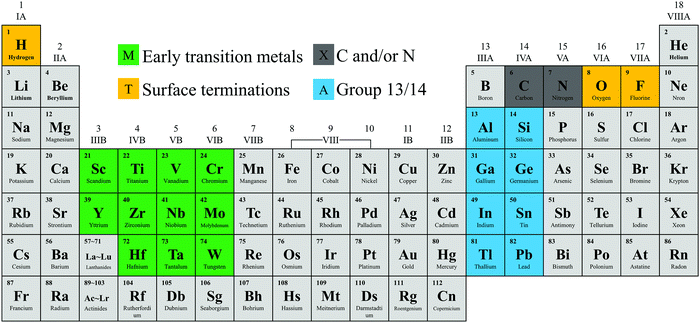
Fortunately, MXenes,16–20 a series of 2D transition metal carbides with a general formula of Mn+1XnTx, (as represented in Fig. 1), where M is an early transition metal (e.g. Sc, Ti, Zr, Hf, V, Cr), X is carbon and/or nitrogen, T represents functional groups (such as O, OH, F), and n = 1, 2, or 3, hold huge promise for 2D intrinsic magnetism due to their remarkably rich variety of chemical and structural diversity. Interestingly, MXenes are characterized by distinct magnetic properties, such as ferromagnetic orders with a range of transport behaviors, including metallicity, half-metallicity, and semi-metallicity.6,21–25 For instance, Ti2C and Zr2C are predicted to be ferromagnetic with intrinsic magnetism.26 It is worth noting that antiferromagnetism in MXenes has also been reported in recent years.27–29 Our previous work has demonstrated that Cr2C MXenes is a ferromagnetic half metal, whereas functionalized Cr2C is an antiferromagnetic semiconductor.27 Besides that, there is another type of MXenes, known as double transition metal (DTM) MXenes.30,31 The general formula of DTM MXene is MnM′2Xn+1Tx. There is no experimentally synthesized or theoretically predicted nitride DTM MXene to date; thus, X only represents carbon in the formula. On the other hand, in DTM MXenes, transition metals are separated in different atomic planes, where inner M layers are sandwiched by outer M′ layers.30 The choice of outer M′ layers is crucial for the design.32 Recently, DTM MXenes VCr2C2(OH)2, VCr2C2F2, and VCr2C2O2 have been proven to be ferromagnets, while TiCr2C2F2 and TiCr2C2(OH)2 are antiferromagnets.28 It is interesting to note that V2C MXene shows no magnetism, whereas DTM VCr2C2(OH)2, VCr2C2F2, and VCr2C2O2 exhibit ferromagnetism.26,28 Moreover, Ti2C energetically favors ferromagnetic ground states, while the favorable magnetic order for DTM TiCr2C2F2 and TiCr2C2(OH)2 is antiferromagnetic.26,28 Very recently, a magnetic glass transition in TiCr2C2Tx was achieved experimentally.33 Therefore, Cr might play a key role in the intrinsic magnetism in DTM MXenes, which makes a prudent design of Cr-based DTM MXene of great interest and importance.
 |
| | Fig. 1 Periodic table showing compositions of MAX phases and MXenes. | |
By considering the abovementioned theoretical predictions as well as the strongly spin-polarized Cr atoms, in this study, we selected Cr layers as the outer M′ layers to design a family of Cr-based DTM MXenes in the chemical formula MCr2CTx, where M = Sc, Y, Ti, Zr, Hf, V, Nb, Ta, Mo, or W, and T = H, O, F, OH, or bare. Comprehensive investigations were performed for these 50 DTM MXenes. Ultimately, we have screened four FM half-metals, ten AFM semiconductors, and one AFM half-metal, which possess moderate band gaps and high estimated Curie/Néel temperatures, implying their enormous potential as spintronic materials.
2. Computational details
We studied the DTM MXenes based on spin-polarized density functional theory (DFT) calculations, which were adopted using the ALKEMIE platform34,35 together with the Vienna ab initio simulation package (VASP).36,37 The interaction between ions and electrons was described by the projector augmented-wave (PAW) method.38 The generalized gradient approximation (GGA) with Perdew–Burke–Ernzerhof (PBE)39 formalism was employed to describe the electron exchange–correlation functional. GGA+U method was adopted to describe the strong-correlation effects for Ti and Cr atoms.40 Since the U values (3 eV) for Ti and Cr are widely used in previous MXene-related theoretical studies, we adopted 3 eV for Ti and Cr in our calculations.27,31,33,41–43 The vacuum space and cutoff energy were chosen to be 20 Å and 550 eV. K-points of 11 × 11 × 1 were automatically generated by Monkhorst–Pack with Γ symmetry for structural optimizations and static calculations. The convergence criteria of both electrons and ions were 1 × 10⁻⁶ eV. We introduced the Heyd–Scuseria–Ernzerhof (HSE06)44 hybrid density functional to precisely calculate the band gaps of DTM MXenes.
To investigate the magnetic properties quantitatively, the classical Heisenberg model was adopted to describe magnetic exchange interactions between Cr atoms, which can be expressed by the following equation:9,45
| | 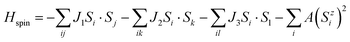 | (1) |
where
J1 is the intra-plane magnetic exchange coupling parameter between sites
i and
j,
J2/
J3 are the inter-plane magnetic exchange coupling parameters between
i and
k/
l,
S is the net magnetic moment of Cr atoms, and
A is an anisotropy energy constant. Herein, by mapping the total energies of DTM MXenes for FM, AFM1, AFM2, and AFM3 states, the exchange coupling constants can be written as the following equations:
32| | | EFM = E0 − (6J1 + 3J2 + 3J3)|S|2 − A|S|2 | (2) |
| | | EAFM1 = E0 − (6J1 − 3J2 − 3J3)|S|2 − A|S|2 | (3) |
| | | EAFM2 = E0 − (−2J1 + J2 − 3J3)|S|2 − A|S|2 | (4) |
| | | EAFM3 = E0 − (−2J1 − J2 − 3J3)|S|2 + A|S|2 | (5) |
By solving the above equations, we can evaluate the magnetic exchange parameters
J1,
J2, and
J3, and thus perform spin dynamics to estimate the Curie/Néel temperature (
TC/
TN) of the magnetic DTM MXene materials. A 30 × 30 × 1 supercell honeycomb lattice with periodic boundary conduction was applied to perform the Metropolis Monte Carlo (MC) simulations. For each studied temperature, the simulations for the DTM MXene last for 10
5 MC steps to reach the thermal equilibrium.
TC/
TN can be estimated by locating the temperature at the peak position of the magnetic susceptibility, and the position of mean magnetic moment drastically drops to nearly zero. To establish the reliability of the simulations, we have reproduced the monolayer CrI
3 with the experimental
TC value of 45 K.
13 The mean magnetic moment and the magnetic susceptibility of CrI
3 are plotted in Fig. S1 (ESI
†) by our MC method. And the estimated
TC is 46 K, which is in excellent agreement with the experimental
TC value,
13 suggesting the validity of our simulation method.
The spin-dependent transport calculations are performed by density functional theory (DFT) with the nonequilibrium Green's function (NEGF),46 which is implemented in the QuantumWise Atomistix Toolkit (QuantumATK) Q-2021.06 package.47 The exchange and correctional interactions of electrons were described by the GGA-PBE form functional, with a linear combination of atomic orbitals (LCAO) norm-conserving PseudoDojo pseudopotential.48 The double-zeta basis set used to expand wave functions was performed for the calculations. The exchange–correlation potential was described based on the GGA+U approach, and the on-site effective interaction parameter U = 3.0 eV is used for d-electrons of Cr atoms.6,40 DFT-D3 method was employed to deal with the interlayer van der Waals force.49 The plane-wave cutoff is 105 hartree, and the average numerical tolerance was less than 10−6 eV for the self-consistent calculation. The Monkhorst k-point mesh for the self-consistent calculation is 10 × 10 × 100. The left and right electrode temperatures are set to 300 K. To ensure the accuracy of the calculated results, a 151 × 151 Monkhorst–Pack grid is used for the spin-resolved transmission coefficient calculation.
3. Results and discussion
3.1. Structure and magnetism screening
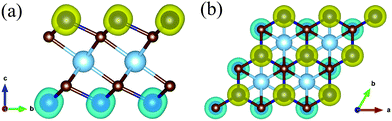
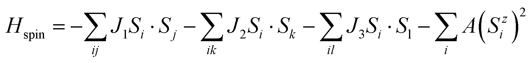
MXenes are usually etched from their bulk MAX phase in hydrofluoric acid (HF) solution, where A represents group 13 and 14 elements from the periodic table (e.g. Si, Al, Ge or Sn).16,50 Thus, the surface of MXenes is often terminated by O, F, and/or OH.21,51 It has been recently reported that the bare MXenes (without surface termination) were fabricated successfully.52 To date, eleven M2C MXenes (Sc2C, Y2C, Ti2C, Zr2C, Hf2C, V2C, Nb2C, Ta2C, Cr2C, Mo2C, W2C) have been theoretically predicted or synthesized experimentally.53–55 Therefore, we consider four functional groups (H, O, OH, F) and bare MXenes based on all these M2C MXenes to design Cr-based DTM MXenes in the chemical formula of MCr2CTx (M = Sc, Y, Ti, Zr, Hf, V, Nb, Ta, Mo, W) in the present study (resulting in a total of 50 MXenes). There are three possible atomic configurations for the terminations on MXene, as depicted in Fig. 2: up and down terminations located toward the C atoms (marked as Model I); up and down terminations positioned above the middle M atoms (marked as Model II); and up terminations located above the C atoms and down terminations located on the middle M atoms (marked as Model III), i.e., a mixture of Model I and Model II. Since magnetic states may affect the stability of the structures, we considered these three DTM MCr2CTx models with nonmagnetic (NM), ferromagnetic (FM), and three antiferromagnetic (AFM) orders, as displayed in Fig. 3.
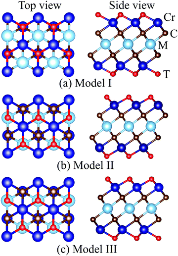 |
| | Fig. 2 Top and side views of different termination configuration models for DTM MCr2CTx. | |
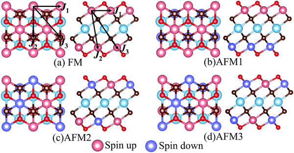 |
| | Fig. 3 Top and side views of possible magnetic order configurations for DTM MCr2CTx: (a) FM, (b) AFM1, (c) AFM2, (d) AFM3. The spin exchange paths are marked in (a). | |
Full geometry optimizations were performed for DTM MCr2CTx with all the three termination configuration models and different magnetic orders to evaluate the energetically favorable atomic arrangements. The calculated energies for the most stable models and preferred magnetic orders of DTM MCr2C2Tx are summed up in Tables S1–S10 (ESI†). The results show that the spin-unpolarized states present higher total energy than spin-polarized states for all the DTM MCr2CTx, and the energy difference between spin-unpolarized and spin-polarized states can reach as high as 2–3 eV per Cr atom. For the three termination configuration models, Model II is the energetically preferred atomic arrangement for a majority of the DTM MCr2CTx, regardless of NM, FM, or AFM states; only 22 MXenes in all the investigated 200 MXenes were the exception (highlighted with blue background in Tables S1–S10, ESI†). Moreover, FM or AFM1 arrangements are the energetically favorable configurations for all the explored DTM MXenes, except for ScCr2C2O2 and YCr2C2O2, which prefer the AFM3 magnetic arrangements. Such results agree well with previous MXene-related works.21,28,56
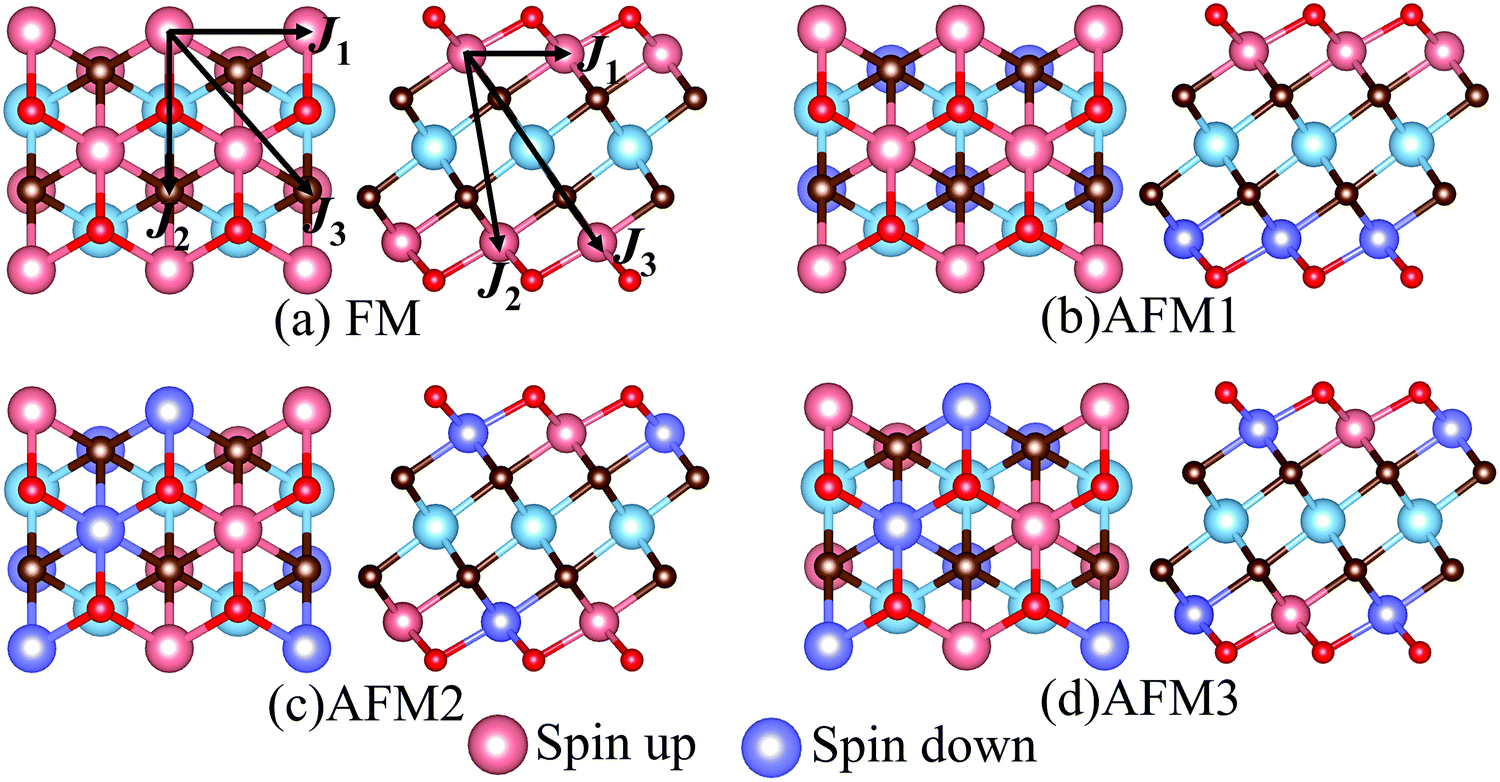
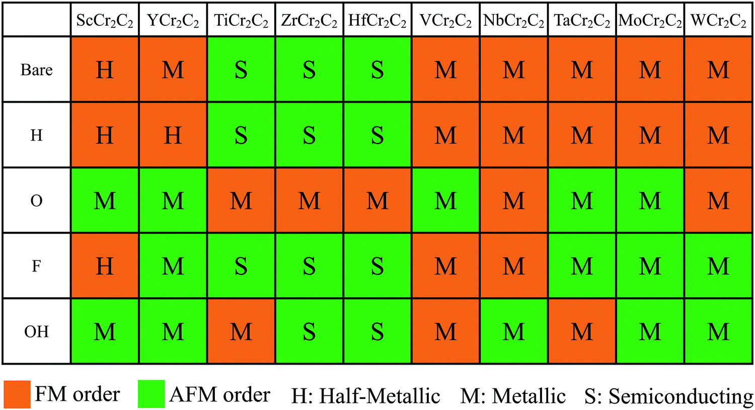
To evaluate the stable magnetic orders, the ground state magnetic ordering for DTM MCr2C2T2 is summarized in Fig. 4. As shown, all the H-terminated DTM MXenes have the same magnetic ground states as the corresponding bare MCr2C2 MXenes. For example, YCr2C2H2 and YCr2C2 prefer the same FM states, while the other surface functional terminations (O, OH, F) do not present a clear pattern. Furthermore, Fig. 4 illustrates the transport behaviors for DTM MCr2C2T2 as well. It can be concluded that the transport behavior of MCr2C2T2 shows sensitive dependence on the center M layers. For example, all the VB and VIB DTM MXenes MCr2CTx (M = V, Nb, Ta, Mo, W) are metallic regardless of the surface terminations, among which 16 MXenes prefer FM state, with the other 9 MXenes taking AFM states as the stable magnetic orders. For a vivid view, Fig. S2–S6 (ESI†) plots the density of states (DOS) of these VB and VIB DTM MXenes. As is displayed, for the majority of the MXenes, the states at Fermi level are mainly occupied by d orbits from Cr and M atoms, while C-2p orbits and the orbits from functional groups make very little contribution. On the other hand, the IIIB and IVB DTM MXenes MCr2CTx (M = Sc, Y, Ti, Zr, Hf) exhibit diverse magnetic orders and transport behaviors, some of which are FM half-metallic, AFM semiconducting, and AFM half-metallic. Herein, the energy band diagrams of magnetic semiconductor and half metal are displayed in Fig. 5. The corresponding DOS of these IIIB and IVB DTM MXenes are presented in Fig. S7–S11 (ESI†), among which 9 MXenes are in FM ground state, while the other 16 MXenes are AFM ground states. The detailed analyses of the magnetic properties for these novel DTM MCr2CTx MXenes are presented in the following.
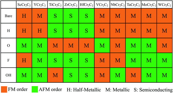 |
| | Fig. 4 Summary of ground state magnetic orderings and transport behaviors for MCr2C2T2 (M = Sc, Y, Ti, Zr, Hf, V, Nb, Ta, Mo, W; T = H, O, F, OH, or bare). The orange and green background correspond to FM and AFM orders, respectively. The letters H, M, and S represent half-metallic, metallic, and semiconducting transport behavior, respectively. | |
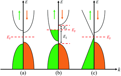 |
| | Fig. 5 Energy band diagrams for magnetic (a) semiconductor, (b) half metal, and (c) Dirac half metal. | |
3.2. FM half-metallic properties
Half-metals were first reported by de Groot. They present a metallic DOS at the Fermi level in one spin direction and a finite band gap in another spin direction.57 The remarkable feature of half-metallic materials is 100% spin polarization with high-efficiency spin injection, giving enormous potential for spintronic devices, such as electrode materials for magnetic tunneling junctions and spin field-effect transistors.58,59 Previous studies have demonstrated that the introduction of an electric field or edge modification to graphene can realize 100% spin polarization; however, these will add difficulty for application and fabrication in practice.60,61 Therefore, the search for intrinsically half-metallic 2D materials with high Curie temperature is highly desired.
Significantly, in the investigated DTM MCr2CTx MXenes, ScCr2C2, ScCr2C2H2, ScCr2C2F2, and YCr2C2H2 exhibit FM half-metallic features. Their calculated minority-spin band gap and half-metallic band gap from the PBE+U and HSE06 method are summarized in Table 1. Herein, the half-metallic band gaps are evaluated by the energy difference between the Fermi level and the nearest minority-spin band around the Fermi level,22i.e., the minimum of E1 and E2 in Fig. 5(b), which is crucial for preventing a magnetic spin flip transition. As displayed in Table 1, the HSE06 approach provides much higher minority-spin band gap than the PBE+U method, ranging from 1.15 eV to 2.38 eV. Moreover, the half-metallic band gaps of ScCr2C2 and ScCr2C2F2 are 0.80 eV and 0.45 eV, respectively, from the HSE06 functional. Such values are comparable with those for double perovskites.58 As discussed, these four DTM MXenes hold enormous promise as spintronic devices, especially ScCr2C2 and ScCr2C2H2, which possess high half-metallic band gap and moderate minority-spin band gap.
Table 1 The calculated minority-spin band gaps (eV) and half-metallic band gaps (eV) of DTM MXenes ScCr2C2, ScCr2C2H2, ScCr2C2F2, and YCr2C2H2 by PBE+U and HSE06 methods
| Structures |
PBE+U |
HSE06 |
| Minority-spin |
Half-metallic |
Minority-spin |
Half-metallic |
| ScCr2C2 |
1.35 |
0.03 |
2.38 |
0.80 |
| ScCr2C2H2 |
0.75 |
0.22 |
1.48 |
0.21 |
| ScCr2C2F2 |
1.15 |
0.04 |
1.99 |
0.45 |
| YCr2C2H2 |
0.34 |
0.03 |
1.15 |
0.15 |
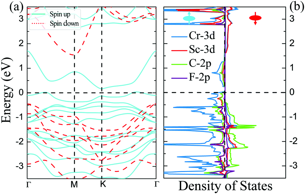
The magnetic and electronic properties of these four DTM MXenes are further explored. Taking ScCr2C2F2 as an example, the spin-dependent electronic band structure and spin-resolved density of states of ScCr2C2F2 by HSE06 approach are illustrated in Fig. 6. As presented, the band structure exhibits metallic character as the bands slightly cross the Fermi level in one spin channel, while for the other channel, a wide indirect band up of 1.99 eV is observed with the conduction band minimum (CBM) and valence band maximum (VBM) located at the M and Γ points, respectively. The CBM is mainly donated by 3d orbits from Cr and Sc atoms, and the VBM is predominately contributed by 2p and 3d orbits from C atoms and Sc atoms, respectively. It is worth noting that in major-spin electrons, only one band slightly crosses the Fermi level, and the higher band holds a gap with respect to the crossing band; this may be modulated by doping or strain engineering to propose a FM semiconducting material.56 The spin-dependent band structure and DOS of ScCr2C2, ScCr2C2H2, and YCr2C2H2 are plotted in Fig. S12–S14 (ESI†), respectively, which show very similar electronic and magnetic features to ScCr2C2F2.
 |
| | Fig. 6 (a) Spin-dependent electronic band structure and (b) spin-resolved density of states of ScCr2C2F2 obtained by HSE06 approach. | |
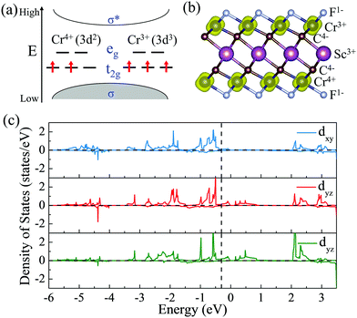
To give further insight into the intrinsic magnetic properties, Fig. 7 illustrates the band diagram model and spin density for ScCr2C2F2. As is shown, one Cr atom donates one 4s electron and three 3d electrons, and the other Cr atom contributes one 4s electron and two 3d electrons to the surrounding C and F atoms, while the Sc atom supplies two 4s electrons and one 3d electron to C atoms, resulting in the nominal oxidation states (Cr4+, Cr3+, Sc3+) and reduction states (C4−, F1−). Hence, in the energy range from oxidation states to reduction states, the bonding σ orbits are fully occupied, with the anti-bonding σ* orbits remaining empty.6,62 However, these orbits’ influence on the magnetic behavior is very limited.43 The energy states between the bonding and anti-bonding orbits are responsible for the electronic and magnetic properties, especially the partially filled Cr non-bonding 3d orbits. In this situation, the octahedral crystal field composed of Cr atoms under D3d symmetry and the nearest surrounding C and F atoms break the non-bonding 3d orbits’ degeneracy, splitting into two bands: the high energy states eg (dx2−y2 and dz2) and the lower band t2g (dxy, dyz and dxz). In the equilibrium ScCr2C2F2 structure, transition metal Sc atoms have little effect on magnetic properties due to their electronic arrangements [Ar]3d0, leaving empty states of Sc d orbits, while the other transition metal Cr atoms play a vital role in the magnetic behaviors. The electronic arrangements of Cr atoms are [Ar]3d2 and [Ar]3d3, leading to two and three electrons in the non-bonding states of Cr atoms, respectively. According to Hund's rule, electrons will primarily fill the lower energy states; thus, the remaining electrons will partially occupy the t2g bands, resulting in two electrons from one Cr atom filling two orbits of the t2g band, and the other Cr atom's three electrons half-occupy each t2g orbit. Taken together, a local spontaneous magnetic moment of 5μB for the two Cr atoms is induced. Evidently, the magnetic moment by our DFT calculation is ∼5μB (2.5μB per Cr atom), implying the validity of the above physical model depicted in Fig. 7. As the PDOS of Cr displays in Fig. 7(c), the dxy, dyz and dxz orbitals show similar orbital split: the spin-up orbitals are occupied, while the spin-down orbitals are empty. These nearly half-occupied orbitals are consistent with our physical mode in Fig. 7(a). Furthermore, the stability of ScCr2C2F2 has been assessed by ab initio molecular dynamics (AIMD) calculations. As the results present in Fig. S15 (ESI†), the atoms are well maintained around their equilibrium positions at 9 ps, and the total energy shows little variation in time from 0 to 9 ps at 300 K, indicating the stability of ScCr2C2F2.
 |
| | Fig. 7 (a) The band diagram model that predicts the magnetic properties of ScCr2C2F2. (b) Side views of spin density for ScCr2C2F2 MXenes. (c) Partial density of states (PDOS) of the Cr dxy, dyz, and dxz orbitals in ScCr2C2F2. | |
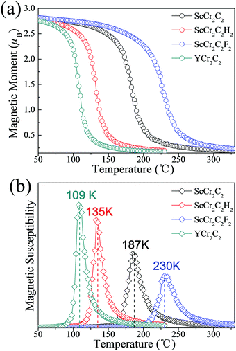
To guarantee stability during practical application as spintronic devices, we further extended the investigations of these four half-metallic MXenes to the Curie temperature (TC) by MC simulation. The total energy differences of various magnetic states and magnetic coupling parameters are listed in Table 2. The positive J1 and J2 values favor ferromagnetic alignment. The simulated magnetic moment and magnetic susceptibility as a function of temperature are displayed in Fig. 8. As presented in Table 2 and Fig. 8(b), the calculated TC values for ScCr2C2, ScCr2C2H2, ScCr2C2F2, and YCr2C2H2 are 187 K, 135 K, 230 K, and 109 K, respectively. Note that the calculated TC values for the four half-metallic MXenes are significantly higher than those ever reported, e.g., 45 K for CrI3 monolayers and 30 K for Cr2Ge2Te6 bilayers.13,14
Table 2 The total energy differences of FM with different AFM states (EFM–AFM, meV) for DTM half-metallic MXenes in a 2 × 1 × 1 supercell, the magnetic coupling parameters (J1, J2, J3, meV) according to the Heisenberg model, and the calculated TC (K) by MC method
| Materials |
E
FM–AFM1
|
E
FM–AFM2
|
E
FM–AFM3
|
J
1
|
J
2
|
J
3
|
T
C
|
| ScCr2C2 |
−306 |
−679 |
−837 |
4.833 |
1.958 |
0.875 |
187 |
| ScCr2C2H2 |
−111 |
−563 |
−650 |
3.826 |
1.375 |
−0.347 |
135 |
| ScCr2C2F2 |
−438 |
−371 |
−556 |
1.698 |
4.327 |
−0.271 |
230 |
| YCr2C2H2 |
−132 |
−567 |
−572 |
3.492 |
0.953 |
0.272 |
109 |
 |
| | Fig. 8 (a) Magnetic moment of Cr atoms and (b) magnetic susceptibility as a function of temperature for ScCr2C2, ScCr2C2H2, ScCr2C2F2, and YCr2C2H2. | |
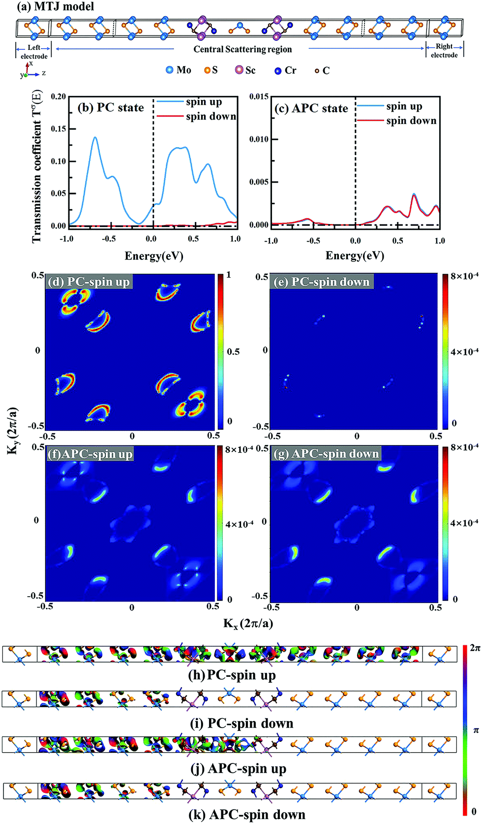
Current-perpendicular-to-plane magnetic tunnel junction (CPP-MTJ) is regarded as one of the most significant spintronics devices, attracting global attention from both the theoretical and experimental points of view.63–65 Due to the weak vdW interaction between the 2D materials in CPP-MTJs, the influence of the electronic structure of half-metallic monolayer is limited, which leads to the significant tunnel magnetoresistance properties. By taking ScCr2C2 as an example, we designed a vdW CPP-MTJ based on ferromagnetic half-metals to estimate the spintronic applications of these DTM MXenes. Fig. 9(a) illustrates the atomic structure of the ScCr2C2-based vdW CPP-MTJ, which is constructed by two electrode layers of 1T-MoS2, a ferromagnetic layer of ScCr2C2, and a tunnel barrier layer of 2H-MoS2. Herein, the optimized lattice constants are 3.191 Å for both 2H-MoS2 and 1T-MoS2, which possess only 1.63% mismatch to monolayer ScCr2C2 (3.244 Å). The metallic and semiconductor properties of 1T-MoS2 and 2H-MoS2 are suitable for functioning as the electrode and tunnel barrier. By applying external magnetic fields, the magnetic configurations for two ScCr2C2 ferromagnetic layers can be implemented: the parallel configuration (PC) and antiparallel configuration (APC). We therefore considered the zero-bias transmission coefficient curves from −1 eV to 1 eV of the ScCr2C2-based vdW MTJ, as plotted in Fig. 9(b) and (c). For the PC state, it can be observed from Fig. 9(b) that there are three significant peak values located at −0.7 eV, 0.3 eV and 0.6 eV in the spin-up channel, and the transmission coefficient at the Fermi level (0 eV) for the spin-up channel  is 0.032. On the other hand, the transmission coefficient curves near the Fermi level are always negligible in the spin-down channel, and the transmission coefficient at the Fermi level for spin-down channel
  is only 5.31 × 10⁻⁷. When the MTJ is in PC state, the transmission coefficients can hardly be detected near the Fermi level for both channels, as is shown in Fig. 9(c). The transmission coefficient at the Fermi level for spin-up channel
  is 8.71 × 10⁻⁶, and that of spin-down channel
  is 9.44 × 10⁻⁶. The tunnel magnetoresistance (TMR) ratio is a very important performance index of MTJ,66,67 which is defined by:
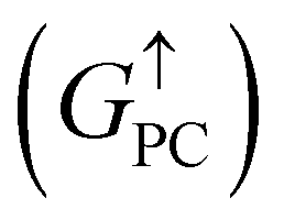
| | | TMR = [(GPC − GAPC)/GAPC] × 100% | (6) |
where
GPC and
GAPC represent total transmission coefficients at the Fermi level of PC and APC states; thus,
,
. Herein, the calculated TMR ratio for the ScCr
2C
2-based vdW MTJ reaches up to 176
000% at zero bias, indicating the promising application of the 1T-MoS
2/ScCr
2C
2/2H-MoS
2/ScCr
2C
2/1T-MoS
2 vdW CPP-MTJ in spintronic devices.
 |
| | Fig. 9 (a) Schematic diagram of 1T-MoS2/ScCr2C2/2H-MoS2/ScCr2C2/1T-MoS2 vdW CPP-MTJ. The zero-bias transmission coefficient curves for MTJ in (b) PC and (c) APC. Spin-dependent transmission spectra for (d) spin-up and (e) spin-down channels of PC, and for (f) spin-up and (g) spin-down channels of APC at zero bias voltage and E = 0 eV. The contour plot of the transmission eigenstates for (h) spin-up and (i) spin-down channels of PC, and for (j) spin-up and (k) spin-down channels of APC at E = 0 eV and (kx, ky) = (0.34, 0.18). | |
To understand more details about the transmission behavior of the ScCr2C2-based vdW CPP-MTJ, the spin-dependent transmission spectra and transmission eigenfunctions were calculated. Fig. 9(d)–(g) represent the spin-dependent transmission spectra at the Fermi level for different magnetic configurations as a function of the k-vector in the 2D Brillouin zone perpendicular to the transport direction. The results present that the transmission coefficients are localized on six symmetrical regions along the diagonals in the whole wave vector space for all cases. Interestingly, in PC state, the transmission coefficients of the spin-up channel at these regions are several orders of magnitude larger than those of the spin-down channel. Hence, the spin-polarized electrons of the left electrode are mainly contributed by the spin-up electrons, which could pass through the barrier layer to the right electrode, corresponding to the ON state of the device. Whereas for APC state, the transmission coefficients of both the spin-up and spin-down channels at these regions are negligible, which result in an extreme suppression of the transmission current, corresponding to the OFF state of the device. Fig. 9(h)–(k) illustrate transmission eigenfunctions for E = 0 eV and (kx, ky) = (0.34, 0.18). As shown in Fig. 9(h) and (j), for both PC and APC states, all the spin-up electrons can pass through the left ScCr2C2 layer and middle 2H-MoS2 barrier layer. The spin-up electrons can only go through the right ScCr2C2 layer for PC state, whereas they are reflected by the right ScCr2C2 layer for APC state. As a result, the transmission eigenstates of the spin-up channel show high value in the whole central region, while those of the spin-down channel are terminated at the right ScCr2C2 layer. On the other hand, as shown in Fig. 9(i) and (k), the transmission eigenstates of spin-down channels are terminated at the left ScCr2C2 layer for both PC and APC states due to the half-metallicity of the ScCr2C2 monolayer. In addition to the transmission eigenstates, the spin-resolved projected local density of states (PLDOS) of the ScCr2C2-based vdW CPP-MTJ in Fig. S16 (ESI†) can also get similar results. As a result, the spin-up electrons in PC state play a decisive role in the spin transport behavior of the ScCr2C2-based vdW CPP-MTJ.
3.3. AFM semiconducting and half-metallic properties
Aside from 2D FM materials, 2D AFM materials are another promising candidate for the next-generation spintronic applications.42 AFM materials exhibit zero magnetic moment due to their ordered magnetic moments taking opposite directions between individual atomic sites. As a consequence, the atoms in AFM materials will not affect each other magnetically; hence, extremely dense elements can be integrated in AFM spintronic devices. Moreover, AFM materials are insensitive to external magnetic fields, hold a fast switching between different magnetic states, and possess intrinsic high frequencies of AFM dynamics.68 Besides the above merits, AFM semiconductors have great potential for nanoscale electronic devices because of the existence of intrinsic band gaps.69
Very attractively, in this work, we found ten AFM semiconductors from the explored DTM MXenes. The M elements of these MCr2C2T2 MXenes are situated at group IVB (M = Ti, Zr and Hf) of the periodic table. We then calculated the band gaps for the ten DTM MXenes, and the results are summed up in Table 3. We can see that HSE06 provides higher band gaps than PBE+U, with the band gaps ranging from 0.56 eV to 1.63 eV. Notably, the band gaps for the spin-up and spin-down channels are not equal in some MXenes; this can be explained by the DOS being asymmetrical in different channels, but the systems exhibit no net magnetization. Deep understanding of the electronic properties has been explored by the spin–dependent band structures and spin-resolved DOSs, as displayed in Fig. S17–S26 (ESI†). All the AFM semiconductors are characterized by indirect band gaps, with most of the VBM located at Γ points, and most of the CBM positioned at M points. In detail, their VBM are mainly occupied by 3d orbits of Cr atoms, while the CBM are contributed by d orbits from Cr and middle transition atoms. Note that all the AFM semiconductors prefer AFM1 arrangement as the ground state. Fig. 10 shows the spin density of TiCr2C2 at the AFM magnetic configurations as an example. Obviously, the Cr atoms completely donated the magnetic moments, and the nearest interlayer Cr atoms are antiferromagnetically coupled with each other, resulting in the zero magnetic moment in TiCr2C2 MXene.
Table 3 The calculated band gaps (eV) for DTM MXene AFM semiconductors by PBE+U and HSE06 approach
| Structure |
PBE+U |
HSE06 |
| Spin up |
Spin down |
Spin up |
Spin down |
| TiCr2C2 |
0.32 |
0.32 |
0.56 |
0.56 |
| TiCr2C2H2 |
0.51 |
0.53 |
0.99 |
1.00 |
| TiCr2C2F2 |
0.81 |
0.77 |
1.47 |
1.41 |
| ZrCr2C2 |
0.31 |
0.37 |
0.56 |
0.64 |
| ZrCr2C2F2 |
0.72 |
0.87 |
1.33 |
1.52 |
| ZrCr2C2(OH)2 |
0.31 |
0.31 |
0.64 |
0.64 |
| HfCr2C2 |
0.28 |
0.24 |
0.53 |
0.51 |
| HfCr2C2H2 |
0.61 |
0.61 |
1.02 |
1.02 |
| HfCr2C2F2 |
0.94 |
0.92 |
1.63 |
1.62 |
| HfCr2C2(OH)2 |
0.32 |
0.32 |
0.61 |
0.61 |
 |
| | Fig. 10 (a) Side view and (b) top view of the spin density of TiCr2C2 MXene. The yellow and cyan colors represent spin-up and spin-down orientations, respectively. | |
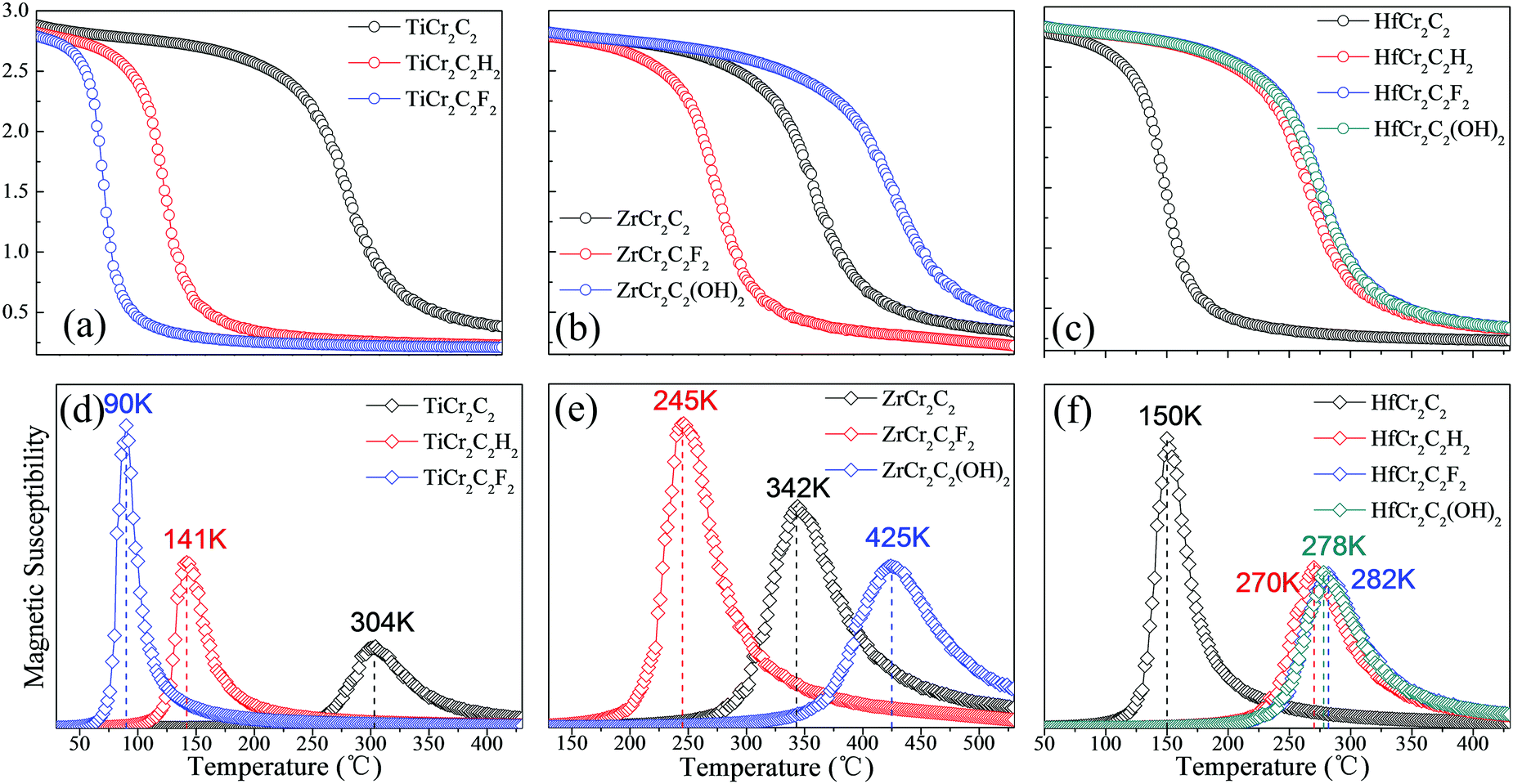
We have further calculated the Néel temperature of the AFM DTM MXenes by MC simulations. The magnetic exchange parameters J1, J2, and J3 have been firstly evaluated in Table 4; thus, by performed spin dynamics, the estimate Néel temperature can be estimated. The magnetic moment of Cr atoms and their magnetic susceptibility as a function of temperature are presented in Fig. 11. The corresponding TN values range from 90 K to 425 K, as summed up in Table 4 and Fig. 11. Generally, the three ZrCr2C2Tx MXenes have a relatively higher Néel temperature than the three TiCr2C2Tx and the four HfCr2C2Tx MXenes. Significantly, the ZrCr2C2(OH)2 MXene holds the highest TN above room temperature due to its large energy difference between AFM1 and FM magnetic orders.
Table 4 The total energy differences of AFM1 with FM (EAFM1–FM, meV), AFM2 (EAFM1–AFM2, meV), and AFM3 (EAFM1–AFM3, meV) states for ten AFM semiconducting MXenes and half-metal ZrCr2C2H2 in a 2 × 1 × 1 supercell, the magnetic coupling parameters (J1, J2, J3, meV) according to the Heisenberg model, and the calculated TN (K) by MC method
| Materials |
E
AFM1–FM
|
E
AFM1–AFM2
|
E
AFM1–AFM3
|
J
1
|
J
2
|
J
3
|
T
N
|
| TiCr2C2 |
−535 |
−426 |
−215 |
6.271 |
−3.639 |
−0.204 |
304 |
| TiCr2C2H2 |
−578 |
−621 |
−280 |
3.190 |
−1.644 |
−0.949 |
141 |
| TiCr2C2F2 |
−487 |
−779 |
−224 |
3.617 |
0.475 |
−2.549 |
90 |
| ZrCr2C2 |
−548 |
−1552 |
−316 |
6.194 |
4.778 |
−7.704 |
342 |
| ZrCr2C2F2 |
−919 |
−935 |
−484 |
4.758 |
−3.253 |
−1.227 |
245 |
| ZrCr2C2(OH)2 |
−1211 |
−391 |
−535 |
4.746 |
−7.326 |
2.373 |
425 |
| HfCr2C2 |
−596 |
−245 |
−343 |
3.260 |
−1.757 |
−2.854 |
150 |
| HfCr2C2H2 |
−892 |
−671 |
−342 |
4.238 |
−3.906 |
0.735 |
270 |
| HfCr2C2F2 |
−956 |
−905 |
−510 |
4.688 |
−3.895 |
−0.827 |
282 |
| HfCr2C2(OH)2 |
−829 |
−658 |
−491 |
3.458 |
−4.598 |
0.051 |
278 |
| ZrCr2C2H2 |
−741 |
−876 |
−342 |
4.357 |
−1.571 |
−1.776 |
165 |
 |
| | Fig. 11 Magnetic moment of Cr atoms and magnetic susceptibility as a function of temperature for (a and d) TiCr2C2Tx, (b and e) ZrCr2C2Tx, and (c and f) HfCr2C2Tx AFM semiconductors, respectively. | |
Besides the AFM semiconductors mentioned, there exists another novel magnetic property with AFM arrangement, namely, the AFM half-metal, which was first proposed by van Leuken and de Groot.70 An AFM half-metal not only can transport a 100% spin-polarized charge with zero net magnetization, but also has the feature of generating no macroscopic magnetic field. Hence, AFM half-metals are expected to be an important species of spintronic material with distinct applications, such as probes in spin-polarized scanning tunneling microscopes.71 Conventionally, the electronic structures of AFM materials in spin-up channel and spin-down channel are usually identical with a symmetry relation, which leads to the vanishing of the net magnetic moment. Thus, the conduction electrons are unspin-polarized. By careful selection, one can discover an AFM material with half-metallic feature. In this case, the polarization of the conduction electrons is not in contradiction with the existence of AFM. This class of materials is called half-metallic antiferromagnet. Coincidentally, the sites of opposite spin of some investigated DTM MXenes are not symmetric, as mentioned before. Therefore, a blueprint came to our mind: AFM DTM MXenes in our study may be endowed with this novel property.
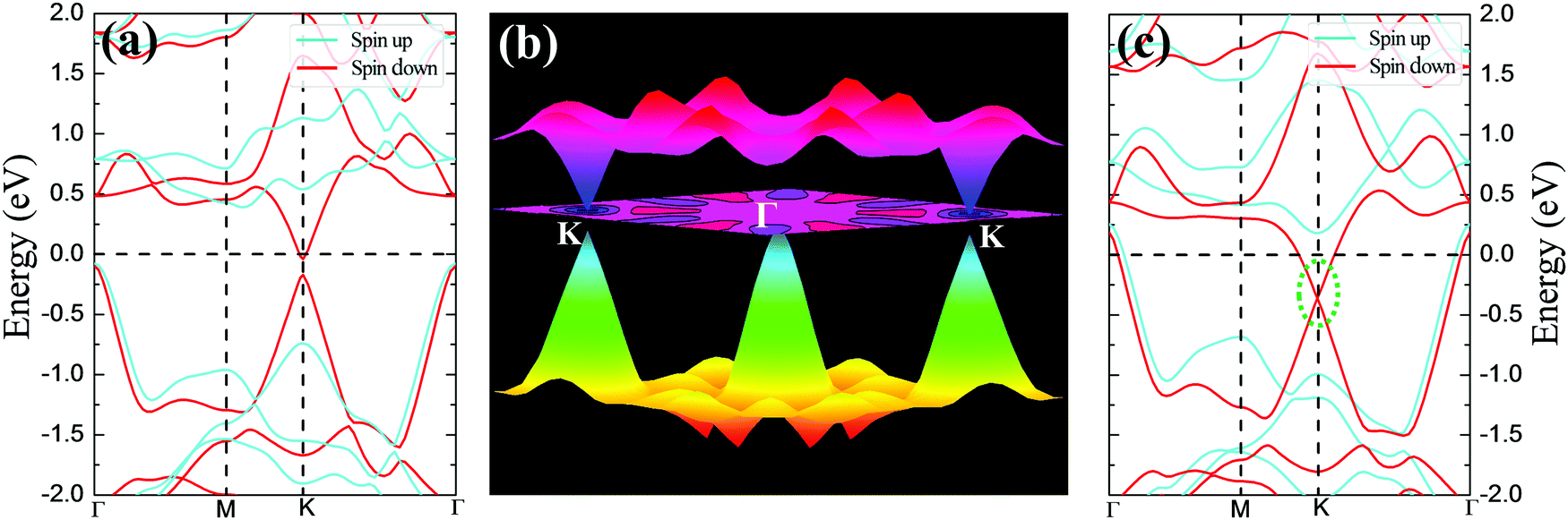
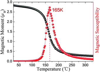
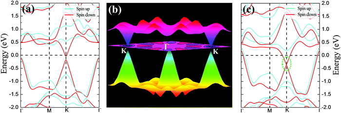
Excitingly, intrinsic AFM half-metallic property was characterized in DTM ZrCr2C2H2 from our screening. The energy differences between different states are listed in Table 4, and the AFM1 magnetic arrangements are the preferred configurations for ZrCr2C2H2. Fig. 12 presents the magnetic moment of Cr atoms and magnetic susceptibility as a function of temperature for ZrCr2C2H2 based on the exchange constants from Table 4, from which one can see that the estimated TN value can reach as high as 165 K. Moreover, as the spin-dependent band structure displays in Fig. 13(a), ZrCr2C2H2 shows metallic conduction feature for the spin-down direction, and a finite band gap in the spin-up direction. Hence, we proposed that DTM ZrCr2C2H2 is an AFM half-metal with high Néel temperature.
 |
| | Fig. 12 Magnetic moment of Cr atoms and magnetic susceptibility as a function of temperature for ZrCr2C2H2 AFM half-metal. | |
 |
| | Fig. 13 Spin-dependent band structure of ZrCr2C2H2 under (a) strain-free condition and (c) 5% tensile strain; (b) 3D band profile around the Fermi level corresponding to (a). | |
From Fig. 13(a), another distinct feature of the spin-dependent band structure of ZrCr2C2H2 is a Dirac cone-like structure at the K point, which is reminiscent of the anomalous electronic states observed in graphene and topological insulators.72,73 Around the Dirac cone, the conduction and valence bands touch with linear dispersions on the Fermi level, inducing the so-called Dirac point. The Dirac point is responsible for many peculiar properties, such as high carrier mobility, which is beneficial for the design of high-speed electronic devices.12,72,73 Based on this, a Dirac half-metal has emerged, characterized by conductivity in one spin direction with a Dirac cone in the other direction; the energy band diagrams for Dirac half metal are illustrated in Fig. 5(c). For DTM ZrCr2C2H2, in spin-up channel, a band gap of 0.5 eV is clearly observed, while an opened Dirac cone positions at the K point of the first Brillouin zone. Fig. 13(b) further illustrates the 3D band profile around the Fermi level. Inspired by the fact that strain engineering is often adopted to manipulate the electronic structure of 2D materials, diverse tensile strains were applied on the DTM ZrCr2C2H2 to explore the variation of the Dirac cone-like feature. Interestingly, only a 5% tensile strain can close the gap of the cone at the K point. As displayed in Fig. 13(c), the Dirac point is located ∼0.4 eV below the Fermi level, which indicates that the DTM ZrCr2C2H2 is not a perfect Dirac half-metal. However, with the growing number of MXene family, more Dirac half-metals are expected to be found in other MXenes.74
4. Conclusions
In summary, we have designed and comprehensively studied 50 DTM MXenes MCr2CTx (T = H, O, F, OH, or bare) on the chemical formula of M2C (M = Sc, Y, Ti, Zr, Hf, V, Nb, Ta, Mo, W) by first-principles calculations. Interestingly, the VB and VIB DTM MXenes MCr2CTx show metallic conductivity with AFM or FM magnetic orders. Moreover, various novel magnetic properties have been presented for IIIB and IVB DTM MCr2CTx MXenes. Notably, ScCr2C2, ScCr2C2H2, ScCr2C2F2, and YCr2C2H2 exhibit FM half-metallicity with wide band gaps and high Curie temperatures. The TMR ratio of the proposed 1T-MoS2/ScCr2C2/2H-MoS2/ScCr2C2/1T-MoS2 vdW MTJ can reach up to 176000% at zero bias. Another ten AFM semiconductors with band gaps ranging from 0.56 eV to 1.63 eV and Néel temperatures from 90 K to 425 K have been predicted. In addition, DTM ZrCr2C2H2 is expected to be a half-metallic antiferromagnet, the Néel temperature of which can reach 165 K. Very interestingly, there exists a Dirac-like cone at K points in the ZrCr2C2H2 band structure. Our study has provided a new strategy for developing MXenes as intrinsically magnetic materials and paves the way for application of the MXene family in the field of spintronics.
Conflicts of interest
The authors declare no competing financial interest.
Acknowledgements
This work was supported by the National Natural Science Foundation of China (No. 21973012, 51872017 and 51871009), the Natural Science Foundation of Fujian Province (Grant No. 2021J06011 and 2020J01351), the National Key Research and Development Program of China (No. 2017YFB0701701), and the “Qishan Scholar” Scientific Research Project of Fuzhou University.
References
- X. Li and J. Yang, Natl. Sci. Rev., 2016, 3, 365–381 CrossRef CAS.
- X. Li and X. Wu, Wiley Interdiscip. Rev.: Comput. Mol. Sci., 2016, 6, 441–455 CAS.
- Y. P. Feng, L. Shen, M. Yang, A. Wang, M. Zeng, Q. Wu, S. Chintalapati and C. R. Chang, Wiley Interdiscip. Rev.: Comput. Mol. Sci., 2017, 7, e1313 Search PubMed.
- N. Miao and Z. Sun, Wiley Interdiscip. Rev.: Comput. Mol. Sci., 2021, e1545 Search PubMed.
- K. S. Novoselov, A. K. Geim, S. V. Morozov, D. Jiang, Y. Zhang, S. V. Dubonos, I. V. Grigorieva and A. A. Firsov, Science, 2004, 306, 666–669 CrossRef CAS PubMed.
- H. Kumar, N. C. Frey, L. Dong, B. Anasori, Y. Gogotsi and V. B. Shenoy, ACS Nano, 2017, 11, 7648–7655 CrossRef CAS PubMed.
- R. Nair, I.-L. Tsai, M. Sepioni, O. Lehtinen, J. Keinonen, A. Krasheninnikov, A. C. Neto, M. Katsnelson, A. Geim and I. Grigorieva, Nat. Commun., 2013, 4, 1–6 Search PubMed.
- Z. Zhang, X. Zou, V. H. Crespi and B. I. Yakobson, ACS Nano, 2013, 7, 10475–10481 CrossRef CAS PubMed.
- B. Wang, Q. Wu, Y. Zhang, Y. Guo, X. Zhang, Q. Zhou, S. Dong and J. Wang, Nanoscale Horiz., 2018, 3, 551–555 RSC.
- B. Wang, Y. Zhang, L. Ma, Q. Wu, Y. Guo, X. Zhang and J. Wang, Nanoscale, 2019, 11, 4204–4209 RSC.
- N. Miao, B. Xu, L. Zhu, J. Zhou and Z. Sun, J. Am. Chem. Soc., 2018, 140, 2417–2420 CrossRef CAS PubMed.
- Z. Liu, J. Liu and J. Zhao, Nano Res., 2017, 10, 1972–1979 CrossRef CAS.
- B. Huang, G. Clark, E. Navarro-Moratalla, D. R. Klein, R. Cheng, K. L. Seyler, D. Zhong, E. Schmidgall, M. A. McGuire, D. H. Cobden, W. Yao, D. Xiao, P. Jarillo-Herrero and X. Xu, Nature, 2017, 546, 270–273 CrossRef CAS PubMed.
- C. Gong, L. Li, Z. L. Li, H. W. Ji, A. Stern, Y. Xia, T. Cao, W. Bao, C. Z. Wang, Y. A. Wang, Z. Q. Qiu, R. J. Cava, S. G. Louie, J. Xia and X. Zhang, Nature, 2017, 546, 265–269 CrossRef CAS PubMed.
- Z. Fei, B. Huang, P. Malinowski, W. Wang, T. Song, J. Sanchez, W. Yao, D. Xiao, X. Zhu and A. F. May, Nat. Mater., 2018, 17, 778–782 CrossRef CAS PubMed.
- A. VahidMohammadi, J. Rosen and Y. Gogotsi, Science, 2021, 372, eabf1581 CrossRef CAS PubMed.
- A. D. Handoko, S. N. Steinmann and Z. W. Seh, Nanoscale Horiz., 2019, 4, 809–827 RSC.
- X. Zhan, C. Si, J. Zhou and Z. Sun, Nanoscale Horiz., 2020, 5, 235–258 RSC.
- P. Xiong, B. Sun, N. Sakai, R. Ma, T. Sasaki, S. Wang, J. Zhang and G. Wang, Adv. Mater., 2019, 32, 1902654 CrossRef PubMed.
- Y. Xia, T. S. Mathis, M. Q. Zhao, B. Anasori, A. Dang, Z. H. Zhou, H. Cho, Y. Gogotsi and S. Yang, Nature, 2018, 557, 409–412 CrossRef CAS PubMed.
- M. Khazaei, M. Arai, T. Sasaki, C. Y. Chung, N. S. Venkataramanan, M. Estili, Y. Sakka and Y. Kawazoe, Adv. Funct. Mater., 2013, 23, 2185–2192 CrossRef CAS.
- J. He, P. Lyu and P. Nachtigall, J. Mater. Chem. C, 2016, 4, 11143–11149 RSC.
- J. Zheng, R. He, Y. Wan, P. Zhao, P. Guo and Z. Jiang, Phys. Chem. Chem. Phys., 2019, 21, 3318–3326 RSC.
- M. Zhao, J. Chen, S.-S. Wang, M. An and S. Dong, Phys. Rev. Mater., 2021, 5, 094408 CrossRef CAS.
- J.-J. Zhang, L. Lin, Y. Zhang, M. Wu, B. I. Yakobson and S. Dong, J. Am. Chem. Soc., 2018, 140, 9768–9773 CrossRef CAS PubMed.
- S. Zhao, W. Kang and J. Xue, Appl. Phys. Lett., 2014, 104, 133106 CrossRef.
- C. Si, J. Zhou and Z. Sun, ACS Appl. Mater. Interfaces, 2015, 7, 17510–17515 CrossRef CAS PubMed.
- J. Yang, X. Zhou, X. Luo, S. Zhang and L. Chen, Appl. Phys. Lett., 2016, 109, 203109 CrossRef.
- W. Chen, H. Li, X. Shi and H. Pan, J. Phys. Chem. C, 2017, 121, 25729–25735 CrossRef CAS.
- W. Hong, B. C. Wyatt, S. K. Nemani and B. Anasori, MRS Bull., 2020, 45, 850–861 CrossRef.
- B. Anasori, Y. Xie, M. Beidaghi, J. Lu, B. C. Hosler, L. Hultman, P. R. C. Kent, Y. Gogotsi and M. W. Barsoum, ACS Nano, 2015, 9, 9507–9516 CrossRef CAS PubMed.
- W. Sun, Y. Xie and P. R. Kent, Nanoscale, 2018, 10, 11962–11968 RSC.
- K. Hantanasirisakul, B. Anasori, S. Nemsak, J. L. Hart, J. Wu, Y. Yang, R. V. Chopdekar, P. Shafer, A. F. May and E. J. Moon, Nanoscale Horiz., 2020, 5, 1557–1565 RSC.
- G. Wang, L. Peng, K. Li, L. Zhu, J. Zhou, N. Miao and Z. Sun, Comput. Mater. Sci., 2021, 186, 110064 CrossRef CAS.
- G. Wang, K. Li, L. Peng, Y. Zhang, J. Zhou and Z. Sun, Acta Metall. Sin., 2022, 58(1), 75–78 Search PubMed.
- G. Kresse and J. Furthmüller, Phys. Rev. B: Condens. Matter Mater. Phys., 1996, 54, 11169 CrossRef CAS PubMed.
- G. Kresse and D. Joubert, Phys. Rev. B: Condens. Matter Mater. Phys., 1999, 59, 1758 CrossRef CAS.
- P. E. Blöchl, Phys. Rev. B: Condens. Matter Mater. Phys., 1994, 50, 17953 CrossRef PubMed.
- J. P. Perdew, K. Burke and M. Ernzerhof, Phys. Rev. Lett., 1996, 77, 3865 CrossRef CAS PubMed.
- S. Dudarev, G. Botton, S. Savrasov, C. Humphreys and A. Sutton, Phys. Rev. B: Condens. Matter Mater. Phys., 1998, 57, 1505 CrossRef CAS.
- J. He, G. Ding, C. Zhong, S. Li, D. Li and G. Zhang, Nanoscale, 2019, 11, 356–364 RSC.
- J. He, P. Lyu, L. Z. Sun, Á. Morales García and P. Nachtigall, J. Mater. Chem. C, 2016, 4, 6500–6509 RSC.
- L. Dong, H. Kumar, B. Anasori, Y. Gogotsi and V. B. Shenoy, J. Phys. Chem. Lett., 2017, 8, 422–428 CrossRef CAS PubMed.
- M. Marsman, J. Paier, A. Stroppa and G. Kresse, J. Phys.: Condens. Matter, 2008, 20, 064201 CrossRef CAS PubMed.
- B. Wang, X. Zhang, Y. Zhang, S. Yuan, Y. Guo, S. Dong and J. Wang, Mater. Horiz., 2020, 7, 1623–1630 RSC.
- M. Brandbyge, J.-L. Mozos, P. Ordejón, J. Taylor and K. Stokbro, Phys. Rev. B: Condens. Matter Mater. Phys., 2002, 65, 165401 CrossRef.
- S. Smidstrup, T. Markussen, P. Vancraeyveld, J. Wellendorff, J. Schneider, T. Gunst, B. Verstichel, D. Stradi, P. A. Khomyakov, U. G. Vej-Hansen, M.-E. Lee, S. T. Chill, F. Rasmussen, G. Penazzi, F. Corsetti, A. Ojanperä, K. Jensen, M. L. N. Palsgaard, U. Martinez, A. Blom, M. Brandbyge and K. Stokbro, J. Phys.: Condens. Matter, 2019, 32, 015901 CrossRef PubMed.
- M. J. van Setten, M. Giantomassi, E. Bousquet, M. J. Verstraete, D. R. Hamann, X. Gonze and G.-M. Rignanese, Comput. Phys. Commun., 2018, 226, 39–54 CrossRef CAS.
- S. Grimme, J. Antony, S. Ehrlich and H. Krieg, J. Chem. Phys., 2010, 132, 154104 CrossRef PubMed.
- M. Naguib, O. Mashtalir, J. Carle, V. Presser, J. Lu, L. Hultman, Y. Gogotsi and M. W. Barsoum, ACS Nano, 2012, 6, 1322–1331 CrossRef CAS PubMed.
- M. Khazaei, A. Ranjbar, M. Arai, T. Sasaki and S. Yunoki, J. Mater. Chem. C, 2017, 5, 2488–2503 RSC.
- V. Kamysbayev, A. S. Filatov, H. Hu, X. Rui, F. Lagunas, D. Wang, R. F. Klie and D. V. Talapin, Science, 2020, 369, 979–983 CrossRef CAS PubMed.
- B. Anasori, M. R. Lukatskaya and Y. Gogotsi, Nat. Rev. Mater., 2017, 2, 1–17 Search PubMed.
- S. Li, P. Tuo, J. Xie, X. Zhang, J. Xu, J. Bao, B. Pan and Y. Xie, Nano Energy, 2018, 47, 512–518 CrossRef CAS.
- Q. Zhong, Y. Li and G. Zhang, Chem. Eng. J., 2020, 128099 Search PubMed.
- Y. Zhang, B. Sa, N. Miao, J. Zhou and Z. Sun, J. Mater. Chem. A, 2021, 9, 10882–10892 RSC.
- R. A. Degroot, F. M. Mueller, P. G. Vanengen and K. H. J. Buschow, Phys. Rev. Lett., 1983, 50, 2024–2027 CrossRef CAS.
- K. I. Kobayashi, T. Kimura, H. Sawada, K. Terakura and Y. Tokura, Nature, 1998, 395, 677–680 CrossRef CAS.
- S. Sugahara and M. Tanaka, Appl. Phys. Lett., 2004, 84, 2307–2309 CrossRef CAS.
- Y.-W. Son, M. L. Cohen and S. G. Louie, Nature, 2006, 444, 347–349 CrossRef CAS PubMed.
- S. Dutta, A. K. Manna and S. K. Pati, Phys. Rev. Lett., 2009, 102, 096601 CrossRef PubMed.
- N. C. Frey, A. Bandyopadhyay, H. Kumar, B. Anasori, Y. Gogotsi and V. B. Shenoy, ACS Nano, 2019, 13, 2831–2839 CrossRef CAS PubMed.
- Y. Feng, X. Wu, L. Hu and G. Gao, J. Mater. Chem. C, 2020, 8, 14353–14359 RSC.
- H. Zhou, Y. Zhang and W. Zhao, ACS Appl. Mater. Interfaces, 2020, 13, 1214–1221 CrossRef PubMed.
- T. Song, M. W.-Y. Tu, C. Carnahan, X. Cai, T. Taniguchi, K. Watanabe, M. A. McGuire, D. H. Cobden, D. Xiao and W. Yao, Nano Lett., 2019, 19, 915–920 CrossRef CAS PubMed.
- F. Bonell, T. Hauet, S. Andrieu, F. Bertran, P. Le Fevre, L. Calmels, A. Tejeda, F. Montaigne, B. Warot-Fonrose and B. Belhadji, Phys. Rev. Lett., 2012, 108, 176602 CrossRef CAS PubMed.
- Y. Zhu, X. Guo, L. Jiang, Z. Yan, Y. Yan and X. Han, Phys. Rev. B, 2021, 103, 134437 CrossRef CAS.
- T. Jungwirth, X. Marti, P. Wadley and J. Wunderlich, Nat. Nanotechnol., 2016, 11, 231–241 CrossRef CAS PubMed.
- J.-S. Chai, J.-T. Wang and L.-F. Xu, ACS Appl. Mater. Interfaces, 2020, 12, 9918–9924 CrossRef CAS PubMed.
- H. van Leuken and R. A. de Groot, Phys. Rev. Lett., 1995, 74, 1171–1173 CrossRef CAS PubMed.
- X. Hu, Adv. Mater., 2012, 24, 294–298 CrossRef CAS PubMed.
- X. Zhang, A. Wang and M. Zhao, Carbon, 2015, 84, 1–8 CrossRef CAS.
- B. Sa, J. Zhou, Z. Sun, J. Tominaga and R. Ahuja, Phys. Rev. Lett., 2012, 109, 096802 CrossRef PubMed.
- R. K. Barik and A. K. Singh, Chem. Mater., 2021, 33, 6311–6317 CrossRef CAS.
Footnote |
| † Electronic supplementary information (ESI) available. See DOI: 10.1039/d1nh00621e |
|
| This journal is © The Royal Society of Chemistry 2022 |
Click here to see how this site uses Cookies. View our privacy policy here. 
 *b,
Naihua
Miao
c,
Jian
Zhou
*b,
Naihua
Miao
c,
Jian
Zhou


 is 0.032. On the other hand, the transmission coefficient curves near the Fermi level are always negligible in the spin-down channel, and the transmission coefficient at the Fermi level for spin-down channel
 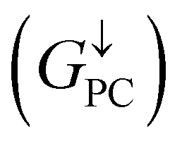 is only 5.31 × 10⁻⁷. When the MTJ is in PC state, the transmission coefficients can hardly be detected near the Fermi level for both channels, as is shown in Fig. 9(c). The transmission coefficient at the Fermi level for spin-up channel
 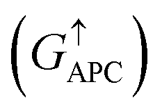 is 8.71 × 10⁻⁶, and that of spin-down channel
  is 9.44 × 10⁻⁶. The tunnel magnetoresistance (TMR) ratio is a very important performance index of MTJ,66,67 which is defined by:
 ,
,  . Herein, the calculated TMR ratio for the ScCr2C2-based vdW MTJ reaches up to 176