 Open Access Article
 This Open Access Article is licensed under a
 Creative Commons Attribution 3.0 Unported Licence
Multi-modal characterization of kesterite thin-film solar cells: experimental results and numerical interpretation
Abdellatif
Saadaldin†
a,
Azat M.
Slyamov†
b,
Michael E.
Stuckelberger
 *c,
Peter S.
Jørgensen
b,
Christian
Rein
b,
Mariana Mar
Lucas
b,
Tiago
Ramos
b,
Angel
Rodriguez-Fernandez
d,
Dominique
Bernard
a and
Jens W.
Andreasen
b
*c,
Peter S.
Jørgensen
b,
Christian
Rein
b,
Mariana Mar
Lucas
b,
Tiago
Ramos
b,
Angel
Rodriguez-Fernandez
d,
Dominique
Bernard
a and
Jens W.
Andreasen
b
aCNRS, Univ. Bordeaux, Bordeaux INP, ICMCB, UMR 5026, F-33600 Pessac, France
bTechnical Univ. of Denmark, DTU Energy, 310, Fysikvej, DK-2800 Kgs. Lyngby, Denmark
cCenter for X-ray and Nano Science CXNS, Deutsches Elektronen-Synchrotron DESY, Notkestr. 85, 22607 Hamburg, Germany. E-mail: michael.stuckelberger@desy.de
dMAX IV Laboratory, Lund University, Box 118, 221 00 Lund, Sweden
First published on 31st March 2022
Abstract
We report a multi-modal study of the electrical, chemical and structural properties of a kesterite thin-film solar cell by combining the spatially-resolved X-ray beam induced current and fluorescence imaging techniques for the evaluation of a fully functional device on a cross-section. The data allowed the correlation of the chemical composition, defects at interfaces and inhomogeneous deposition of the layers with the local charge-collection efficiency of the device. We support our observations with Monte Carlo simulations of high-energy X-ray interactions with the semiconductor device, and finite-volume modeling of the charge-collection efficiency.
1. Introduction
The growing energy demand is currently being addressed with a focus on climate change mitigation, and the development of renewable energy sources.1 Among these, solar energy has the potential of becoming a multi-terawatt technology.2,3 In 2017, crystalline silicon-based photo-voltaic (PV) technology had around 95% of the solar market share due to the well-established silicon industry and the relatively high efficiency and stability of the devices. However, silicon solar modules’ production is not efficient in terms of energy and material consumption.4–6 To become a commercially viable alternative to silicon-based technology, new generations of solar cells have to be competitive in terms of stability, up-scaling and energy-payback time.7 Thin-film PVs are currently being investigated as a promising candidate that could satisfy the requirements mentioned above.One of the emerging thin-film PV technologies is based on kesterite crystal structures such as Cu2ZnSnS4 (copper zinc tin sulfide – CZTS). The advantages of kesterite solar cells is that they can be produced in a low-cost manner and are mostly made of abundant and non-toxic elements. The high absorption coefficient of CZTS, associated with its direct band gap, allows reducing the thickness of the absorber layer to few hundred nanometers, making the technology extremely resource-efficient. However, the most recent studies on laboratory scale CZTS solar cells have shown efficiencies of just above 10%, which is far behind the predicted theoretical limit of 28% for this type of material.8 The possible factors limiting the performance are the presence of undesired phases in the composition of the CZTS absorber layer and defects at the interface of the device layers.9,10 The ability to observe at the nanoscale the influence of these defects on the local performance of a fully functional CZTS device can bring crucial information for understanding spatial correlations between charge-transport mechanisms and defects in the structure of the device.
Synchrotron-based scanning X-ray microscopy is a powerful technique for the spatially resolved high-resolution investigation of solar-cell materials.11,12 The high flexibility of beamlines to incorporate different modalities and the advancement of X-ray optics allow obtaining and uniquely correlating information about different properties of materials at the nanoscale.13–16 Analytical techniques, such as X-ray fluorescence (XRF), X-ray diffraction, ptychography and X-ray beam induced current (XBIC), applied simultaneously can provide spatially correlated information between the chemical composition and electrical properties of the specimen without destroying it.17–22 However, such information is often not sufficient to understand the limitations of energy-harvesting devices. The complex architecture of the new generation solar cells comprising multiple layers makes it hard to determine the fundamental mechanisms impacting the electrical performance. First-principles modeling of the XBIC signal is required to obtain a deeper understanding of the correlations between material properties and the electrical performance of the device. Therefore, XBIC experiments on a semiconductor device combined with modeling has been performed for a single nanowire with a 1D numerical simulation carried out using Comsol Multiphysics software,23 and for a single-junction, CdTe/CdS solar cell with 2D drift-diffusion modeling.24,25
In this paper, we present the results of the multi-modal study of a CZTS solar cell cross-section by employing combined measurements of scanning X-ray analytical techniques for a correlative investigation of the structural, chemical and electrical properties of a fully functional device at the nanoscale. We support experimental data with the finite volume modeling of the XBIC signal by solving Poisson’s equation and the continuity equations for electrons and holes within the 2D computational domain constructed from the XRF data.
2. Experimental
2.1 CZTS solar cell preparation
The solar cell was obtained by the deposition of a Mo bilayer on a soda-lime glass substrate before pulsed-laser deposition of the CZTS precursors. For good adhesion to the substrate, the first 200 nm thick Mo layer was deposited under 1.3 × 10⁻² mbar pressure. For a lower sheet resistance, the second 300 nm Mo layer was deposited under 3.9 × 10⁻³ mbar pressure. CZTS precursors were deposited under high vacuum (5 × 10⁻⁶ mbar) from a sintered target with overall CZTS stoichiometry (2.5 cm diameter, 2CuS![[thin space (1/6-em)]](https://www.rsc.org/images/entities/char_2009.gif) :ZnS:SnS, Testbourne Ltd), resulting in an ultra-thin absorber layer (less than 450 nm). Annealing was performed at 560 °C. On top of the absorber layer, a 60 nm CdS buffer layer was deposited by chemical bath deposition. After that, a 50 nm intrinsic ZnO (i-ZnO) window layer and a 200 nm indium tin oxide (ITO) layer were sputtered by an RF magnetron, followed by a 100 nm MgF anti-reflection coating. A more detailed description of the solar cell fabrication has been reported earlier.26
:ZnS:SnS, Testbourne Ltd), resulting in an ultra-thin absorber layer (less than 450 nm). Annealing was performed at 560 °C. On top of the absorber layer, a 60 nm CdS buffer layer was deposited by chemical bath deposition. After that, a 50 nm intrinsic ZnO (i-ZnO) window layer and a 200 nm indium tin oxide (ITO) layer were sputtered by an RF magnetron, followed by a 100 nm MgF anti-reflection coating. A more detailed description of the solar cell fabrication has been reported earlier.26
A multi-modal study of a single device puts constraints on the sample configuration. In contrast to the common approach of plane-view measurements, the measurements presented hereafter were taken on a cross-section following a similar experimental design as that in ref. 27: XBIC and XRF measurements of a thin lamella on a cross-section of the sample allow observing the collection of charge carriers in the absorber layer on the one hand, and the elemental distribution on the other hand. A 1 μm thick lamella was chosen to match the approximate CZTS grain size determined from preliminary experiments on comparable devices.28,29 Furthermore, the thin sample cross-section allows X-rays to be transmitted and recorded in the far-field regime to derive the differential phase contrast (DPC) using a pixel array detector.30
The investigated CZTS thin-film solar cell was previously characterized by Raman spectroscopy, X-ray diffraction, time-resolved photoluminescence, 3D X-ray diffraction29 and resonant ptychographic tomography.28Fig. 1 (left) shows the device architecture alongside an SEM image of the sample (right) used in the experiment, consisting of a cross-section lamella of ca. 1 μm thickness derived from the solar cell using a focused ion beam (FIB) technique. The lamella was extracted from the best-performing subcell of a device that was sized in the order of 1 cm2. The entire lamella was scanned, and a region containing both homogeneous and defective parts was selected for further analysis.
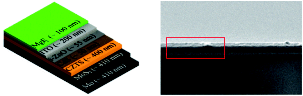 | ||
| Fig. 1 Solar-cell device architecture (left) and SEM image (right) of the cross-section lamella used in the experiment. The red box indicates the area raster-scanned by the focused X-ray beam. | ||
2.2 Analytical techniques
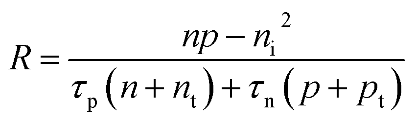
Upon irradiation with X-ray photons whose energy exceeds the electron-binding energy, core-level electrons are excited to a higher state or ejected. Excited atoms relax to the ground state by filling the resulting vacancies with electrons from one of the higher states. Such transitions are accompanied by the emission of fluorescent photons of energies that are characteristic of given types of atoms in the specimen. Two-dimensional maps of the constituent elements can be derived by scanning the specimen and recording the energy of emitted fluorescent photons. The energy spectrum of fluorescent photons at every scanning position is composed of individual peaks directly related to the abundance of atoms of the constituent elements.31The principle of XBIC is similar to that of electron beam induced current (EBIC) in a scanning electron microscope: a current-measuring device connected to the solar-cell electrodes evaluates the X-ray beam induced current. Excess carriers generated by the X-ray beam will diffuse inside the sample, with some of them reaching the edge of the space charge region (SCR) of the p–n junction. The electric field inside the SCR separates electron–hole pairs that give rise to the photo-current in an external circuit. By scanning the X-ray beam, a two-dimensional map of the collected photo-current in the device is constructed.11,18,32,33
2.3 Measurements
The experiment was performed at the NanoMAX, a hard X-ray nanoprobe beamline of the MAX IV synchrotron facility in Lund, Sweden.14 The measurements were carried out under ambient conditions with a 10.4 keV coherent monochromatic X-ray beam. The X-ray energy was chosen to yield fluorescent photons corresponding to the K and L transitions of the elements constituting the sample. The beam was focused by Kirkpatrick-Baez (KB) mirrors to a spot size of 80 nm × 80 nm on the sample. A piezo stage was used to move the sample with 50 nm step size in the plane perpendicular to the beam propagation. An Amptek energy-dispersive fluorescence detector was placed 2 cm away from the sample under approximately 30° relative to the scanning plane to collect fluorescence photons. A photon counting Dectris Pilatus 100k pixel-array detector was located 4 m downstream from the sample to record the diffraction signal of the transmitted photons (Fig. 2). An optical chopper was placed upstream of the sample to modulate the incident X-ray beam with a chopping frequency of 617 Hz. The P and N terminals of the solar cell were connected to the MFLI lock-in amplifier from Zurich Instruments.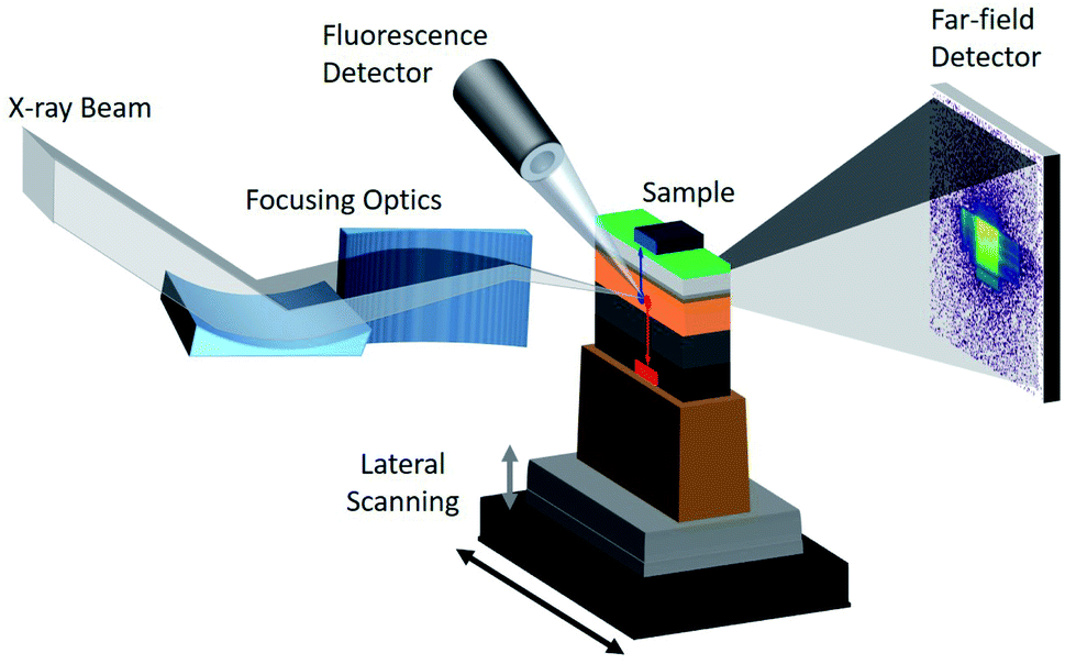 | ||
| Fig. 2 Schematic of the experimental setup. Incoming X-rays are focused using KB mirrors down to 80 nm × 80 nm. The sample is raster-scanned in the lateral plane. A far-field detector measures the diffraction signal of the transmitted beam, and an energy-dispersive fluorescence detector collects fluorescence photons. The X-ray beam induced current in the semiconductor device is amplified and measured at every scan position. | ||
3. Numerical modeling
In this work, a 2D computational domain was generated from the XRF data, and a 2D finite-volume numerical simulation approach was used. In conjunction with the continuity equations for electrons and holes coupled with a Monte Carlo (MC) simulation for the X-ray/material interaction, Poisson’s equation was solved to simulate the XBIC experiment. Simulations were performed on a regular grid defined from the measurements’ step size (50 nm) and taking into account a beam limited to one point. These simplifications were made to be as close as possible to the experiment assuming that the physical processes included in the numerical model were more relevant than the real intensity profile of the experimental beam, the consideration of which would have been beyond the scope of this work.3.1 Electron–hole-pair generation from the X-ray beam
X-ray propagation and interaction with matter are often described using analytical models. This approach might not be sufficient for modeling complex phenomena, and Monte Carlo-based numerical simulations might be more suitable. In general, a Monte Carlo simulation employs known probability distributions of various interactions of X-ray photons with matter to model their propagation within the interaction volume and associated change of their state. We utilized a personalized version of Penelope,34 to simulate the generation of electron–hole pairs in the multi-layered solar cell upon the incidence of the pencil X-ray beam. The resulting profiles of the generation rate G were then used in the modeling of the XBIC signal.3.2 Numerical model
The basic equations to be solved in modeling semiconductor devices are Poisson’s equation and the electrons and holes continuity equation. In steady state, they are expressed as| ∇·(εrε0∇ψ) = q(n − p + NA − ND), | (1) |
| ∇·Jn = −q(G − R), | (2) |
| ∇·Jp = q(G − R), | (3) |
 | (4) |
| Jn = qμn(−n∇ψn + VT∇n), | (5) |
| Jp = qμp(−p∇ψp−VT∇p), | (6) |
 and
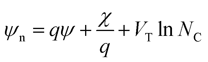
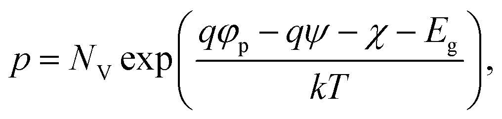
and 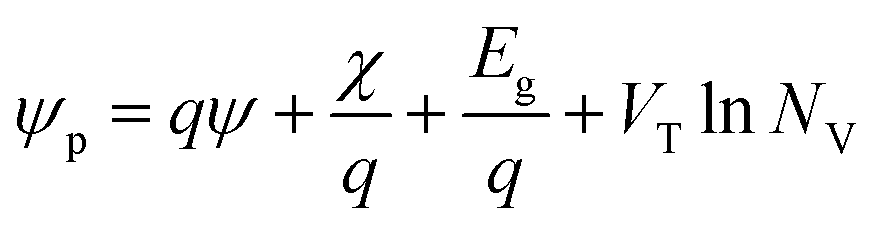 are the effective potentials for electrons and holes, respectively, χ is the electron affinity, Eg is the energy gap, NC, and NV are the effective densities of state in the conduction and valence bands, respectively, and
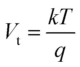
 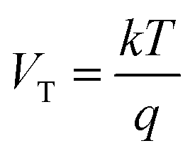 is the thermal potential with the Boltzmann constant k and the temperature T. In eqn (5) and (6), we used the so-called Einstein relation.35 Moreover, since we assumed having only non-degenerate semiconductors, the Boltzmann approximations were used in our simulations to compute the density of carriers as follows:
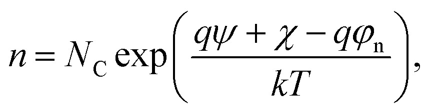 | (7) |
 | (8) |
The choice of boundary conditions will affect the solution of the set of partial differential equations. In our simulations, we considered two types of contacts: ohmic and Schottky contacts. For ideal ohmic contacts, the space charge vanishes at the contact and the interface recombination velocities for electrons and holes (Sn and Sp, respectively) are assumed to be infinite. This will impose the Dirichlet boundary conditions for n and p at the contact. The Dirichlet boundary conditions for the electrostatic potential at ohmic contacts is given by the sum of the externally applied bias V0 and the built-in potential ψbi. The physics of Schottky contacts is complex and we used simplified models. We assumed that the Fermi level in the semiconductor is lined up with the Fermi level of the metal and that the electrostatic potential at the boundary is proportional to the electron barrier height ΦBn. The carrier concentrations at Schottky contacts depend in general on the current density at the contact, which implies that they depend on Sn, Sp and ΦBn.
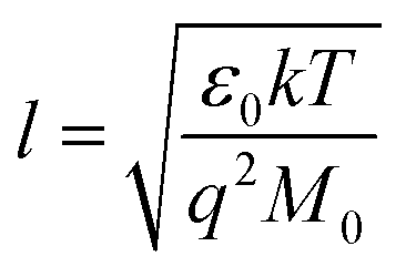
Due to the different orders of magnitude of the dependent variables (ψ, n, p) and to avoid numerical overflow, rewriting the equations in the dimensionless form is necessary. The scaling factors used in the simulations are summarized in Table 1.
| Quantity | Expression | Value |
|---|---|---|
| Concentrations | M 0 | 1025 m−3 |
| Potentials |
|
0.02585 V |
| Length |
|
3.78 × 10⁻¹⁰ m |
| Energy | kT | 0.02585 eV |
| Mobility | μ 0 | 10−4 m2 V−1 s−1 |
| Time |
|
5.53 × 10⁻¹⁴ s |
| Gen., rec. rates |
|
1.81 × 1038 m−3 s−1 |
| Current density |
|
−1.10 × 10¹⁰ A m−2 |
| Velocity |
|
6.84 × 10³ m s−1 |
The finite volume method was used to discretize the linearized Poisson’s equation and the continuity equations. A suitable approximation for the current expressions using the Scharfetter Gummel scheme36 was implemented. The derived coupled nonlinear system was solved using Gummel’s algorithm.37 Current densities were calculated from the resulting solution, and the total current (XBIC signal) was calculated by integrating the local current density over the contact.
4. Results and discussion
4.1 Experimental results
Fig. 3 shows XRF images of the elements constituting the sample and the corresponding XBIC signal. As measurements were performed simultaneously, no registration of the XRF and XBIC images is necessary and per pixel based correlation between images can be performed. The most prominent compositional inhomogeneities within the CZTS layer are highlighted in the images with white arrows. They are associated with relatively lower projected densities of all elements composing the layer (except for S and Mo, which could not be reliably differentiated from each other38). This can be attributed to reduced thickness due to sample preparation or voids between CZTS grains filled with CdS.28 Both factors will result in reduced charge-collection efficiency that is correlated with the relative decrease of the XBIC signal in these regions. A more notable area with inhomogeneous chemical composition is marked with the white box. The corresponding area in the XRF image of Cd indicates CdS precipitates resulting from the chemical bath deposition. It is, however, unclear whether the CdS precipitate resulted in the absence of the ZnO layer deposited on top. Regardless, the XRF images of In and Sn show a variation in the composition of elements constituting the ITO layer that follows the topology of the CdS precipitate. Overall, the XBIC image in the area below the white box shows a decreased current associated with the electronic defects caused by the disturbed layer structure.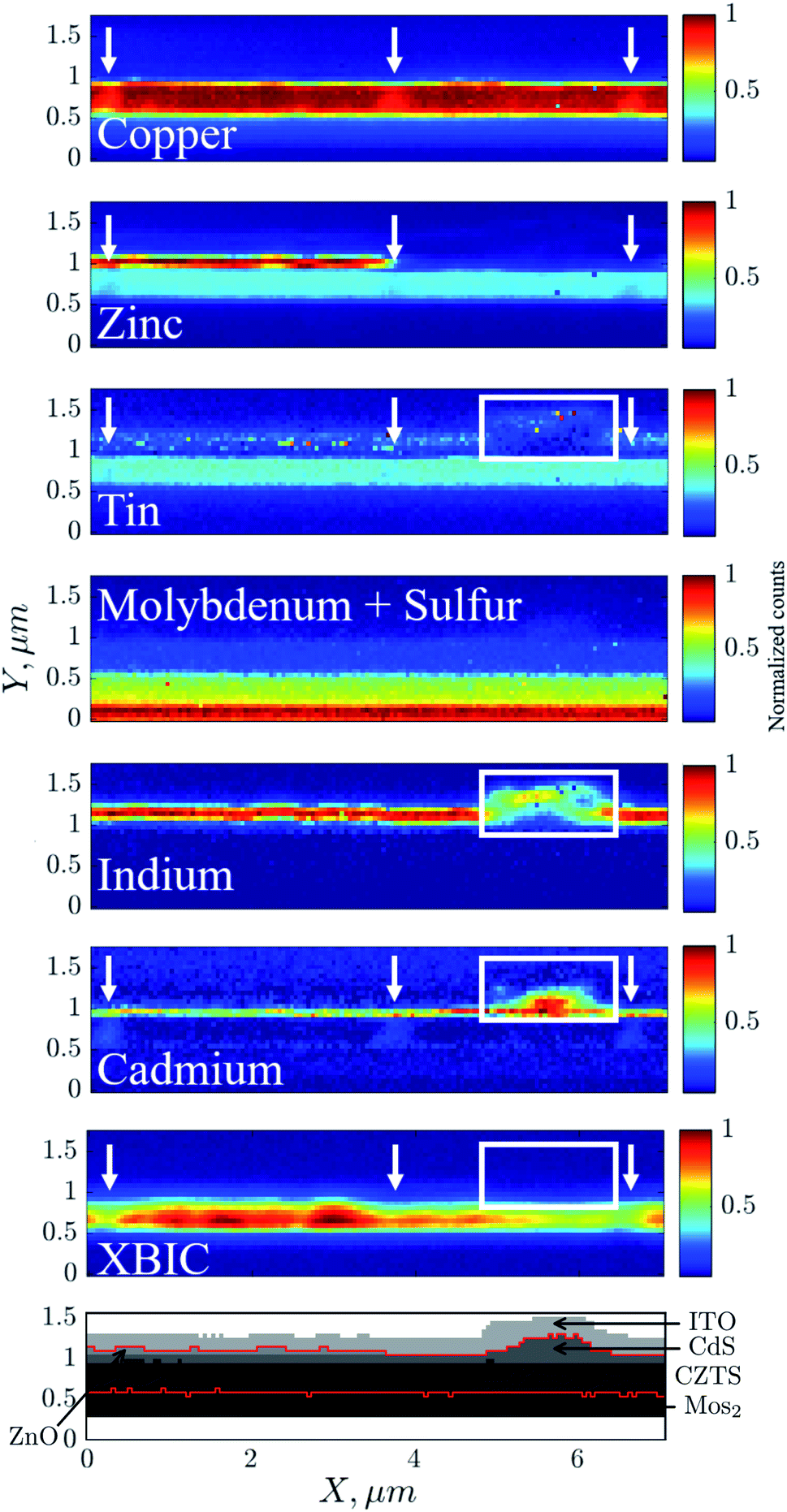 | ||
| Fig. 3 XRF images of the main elements constituting the sample together with the XBIC signal, resulting in the specification of the layered structure with the computational domain between red lines. The white arrows highlight the areas associated with composition variations in the CZTS layer and the white box indicates the area with an inhomogeneous distribution of elements from the CdS and ITO layers, as well as the absence of the ZnO layer. | ||
4.2 Construction of the computational domain
Individual XRF maps of elements constituting the CZTS sample under consideration were used to construct the computational domain. Image pixels were assigned to one of the materials according to the nominal architecture of the device presented in Fig. 1. From the XRF data, the geometry was obtained through the following process. We started from the bottom of the image: Mo will correspond to the pixels having an intensity in the MoS image larger than ξ1, MoS2 to the pixels not yet defined and having an intensity in the MoS image larger than ξ2, CZTS to the pixels not yet defined and having an intensity in the Cu image larger than ξ3, CdS to the pixels not yet defined and having an intensity in the Cd image larger than ξ4, etc. The threshold values ξi were selected manually by combining the six chemical images and examining the interfaces between the different layers. After cleaning the geometry defined from the chemical data, we obtained the grey level image shown as the lowest panel of Fig. 3. The correlation with the ptychographic reconstruction of the phase contrast from far-field diffraction data corroborate the segmentation. At the lower part of the sample, the MoS2 layer was considered as the electrode, and the boundary condition was applied at the interface with the CZTS layer. At the upper part, the ITO layer was considered as the electrode, and the boundary condition was applied at the interface with the ZnO and CdS layers. The resulting computational domain was then composed of the three layers encompassed by a red line in Fig. 3. On the lateral boundaries, we imposed periodicity, and on the upper and lower boundaries, electrical contact with the electrodes.4.3 2D simulations
The computational domain shown in Fig. 4(a) is discretized into 1435 computational cells with 50 nm × 50 nm size, equivalent to the measurement grid. For each cell, a generation profile was derived from the Monte Carlo simulation of a pencil beam with an energy of 10.4 keV interacting with the material associated with each layer. The continuity equations, along with Poisson’s equation were solved for the entire domain for each generation profile, and the resulting total current was stored to construct a 2D map of the XBIC signal. Two types of boundary conditions are considered: ohmic and Schottky contacts. At an ohmic contact, we assume a perfect contact, meaning that there is nothing blocking the carriers from one material to another. Fig. 4(c) shows the result of applying ohmic boundary conditions. From Fig. 4(b), we can clearly see the effect of the lack of a ZnO layer at the right-hand side of the domain (red box) on the experimental data, which is not the case for the simulation results in Fig. 4(c).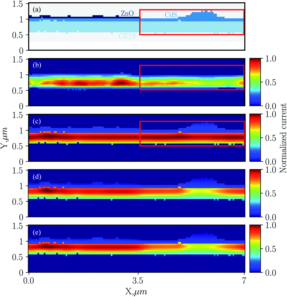 | ||
| Fig. 4 (a) The computational domain based on the XRF measurements shown in Fig. 3, (b) the experimental results and (c) simulation results from applying ohmic boundary conditions, (d) ideal Schottky contact boundary conditions with the material parameters listed in Table 2 and (e) Schottky contact boundary conditions with a work function equal to 5.3 eV for the MoS2 layer and barrier height equal to 0.5 eV at the CdS contact. | ||
At a Schottky contact, we assumed that there is a potential barrier formed at the interface that impedes the transfer of carriers from one material to another. The barrier height of an ideal Schottky contact for an n-type semiconductor is given by the difference between the contact work function and the electron affinity as follows:
| ΦBn = ϕM − χ, | (9) |
| ΦBp = ϕM − χ − Eg. | (10) |
After trying different combinations of ohmic and Schottky boundary conditions, we chose to apply the Schottky boundary condition at the top of ZnO or CdS, and at the bottom of the CZTS region. At the front contact (top of ZnO or CdS), we have an ITO layer with work function ϕM = 4.7 eV,39 and at the back contact (bottom of CZTS) we have a MoS2 layer. Estimating the work function of MoS2 is challenging and we first used the value ϕM = 5 eV in our simulation, which is approximately equal to the work function of Mo.40 The material parameters for each layer used in the simulation are listed in Table 2. These parameters were taken from the literature.41–44Fig. 4(d) shows the simulation results when applying ideal Schottky contact boundary conditions. We start seeing the effect of the lack of a ZnO layer on the simulation results on the right-hand side of the domain. In order to match the experimental results, we did a 2D sensitivity analysis to study the effect of the barrier height at the contact on the simulation results.
| Parameter | Description | Unit | CZTS | CdS | ZnO |
|---|---|---|---|---|---|
| N C | Effective density of state in the conduction band | m−3 | 2.2 × 1024 | 2.2 × 1024 | 2.2 × 1024 |
| N V | Effective density of state in the valence band | m−3 | 1.8 × 1025 | 1.8 × 1025 | 1.8 × 1025 |
| E g | Energy gap | eV | 1.4 | 2.4 | 3.3 |
| χ | Electron affinity | eV | 4.7 | 4.5 | 4.5 |
| ε r | Relative permittivity | — | 10 | 10 | 9 |
| μ n | Electron mobility | m2 V−1 s−1 | 10−2 | 10−2 | 10−2 |
| μ p | Hole mobility | m2 V−1 s−1 | 2.5 × 10⁻³ | 2.5 × 10⁻³ | 2.5 × 10⁻³ |
| τ n | Electron lifetime | s | 2 × 10⁻⁸ | 10−12 | 10−12 |
| τ p | Hole lifetime | s | 10−5 | 5 × 10⁻¹³ | 10−7 |
| N D | Ionized donor density | m−3 | 0 | 1022 | 1023 |
| N A | Ionized acceptor density | m−3 | 3 × 10²² | 0 | 0 |
| S n | Interface recombination velocities for an electron | m s−1 | 105 | 105 | 105 |
| S p | Interface recombination velocities for a hole | m s−1 | 105 | 105 | 105 |
| Φ Bp/ΦBn | Hole/electron barrier height | eV | −1.2 | 0.2 | 0.2 |
4.4 2D sensitivity analysis
In the 2D sensitivity analysis, the results presented in Fig. 4(d) were used as a simulation reference. We studied the effect of the barrier height at the top contact of CdS and at the bottom contact of CZTS.According to ref. 39, ITO forms an ideal Schottky contact with ZnO. From Fig. 3, in the white box, we can see inhomogeneities in the distribution of the elements forming the ITO layer (indium and tin). Therefore, the assumption of an ideal Schottky contact with the CdS layer is an oversimplification as it neglects the existence of surface and interface states. Moreover, Dharmadasa45 reported that the Schottky barrier formation at the CdS contact is found to be governed by Fermi level pinning, depending on the contact and the fabrication process rather than on the work function of the contact. At the bottom contact of CZTS, the work function of MoS2 varies from 5.15 eV to 5.39 eV depending on the thickness of the layer.46
Three different layer configurations are used to present the 2D sensitivity analysis as line profiles. These configurations, denoted as S1, S2 and S3, are presented in Fig. 5(a). In S1, we have the complete layer structure ZnO/CdS/CZTS, in S2 and S3 the ZnO layer is missing, and S3 is on the CdS defect. The effects of changing the barrier height from 0.25 eV to 0.75 eV at the CdS contact are presented in Fig. 5(b, d, and f) along S1, S2 and S3, respectively. Along S1, changing the barrier height at the CdS contact has no effect on the XBIC signal. On the other hand, increasing the barrier height at the CdS contact decreases the XBIC signal along S2 and S3. The presence of the ZnO layer with a barrier height equal to 0.2 eV is essential for the performance of the device under consideration.
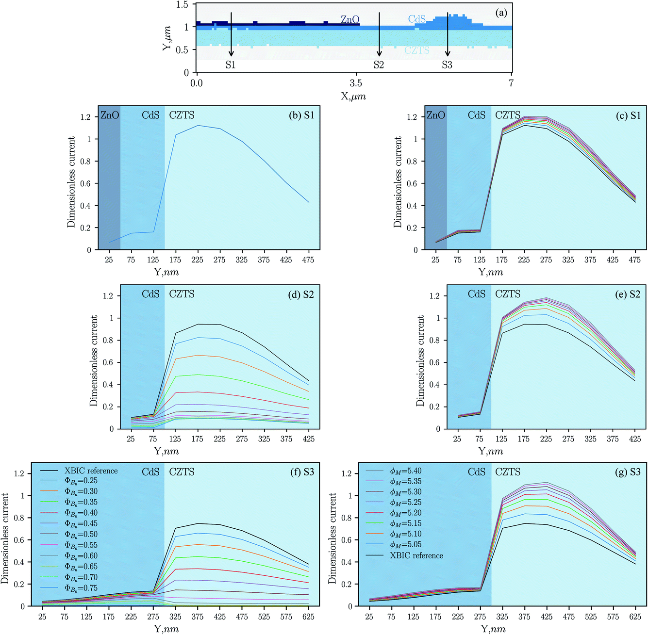 | ||
| Fig. 5 (a) The computational domain with three distinct layer configurations: S1, S2 and S3. (b–g) The 2D sensitivity analysis was done using the material parameters listed in Table 2. The effects of changing the barrier height ΦBn at the CdS contact along S1, S2 and S3 are shown in (b), (d) and (f), respectively, and the effects of changing the work function ϕM of MoS2 along S1, S2 and S3 in (c), (e) and (g), respectively. The legends displayed in (f) and (g) refer to (b, d, and f) and (c, e, and g), respectively. All curves overlap in (b). | ||
Fig. 5(c, e, and g) show the effects of changing the work function of MoS2 from 5.05 eV to 5.4 eV on the XBIC signal along S1, S2 and S3, respectively. The XBIC peak in the CZTS layer shifts upwards with increasing the work function of MoS2 along S1, S2 and S3. Therefore, the presence of the interfacial MoS2 layer with a work function higher than the one in Mo is beneficial for the performance of the device under consideration. This result is in good agreement with the result of ref. 47 and in ref. 40 they found similar behaviour for CZTSe devices.
From Fig. 5, we see clearly that increasing the barrier height for electrons at the CdS contact will reduce the XBIC peak at the right-hand side of the domain. Moreover, decreasing the barrier height for holes by increasing the work function of MoS2 will increase the XBIC peak for the entire domain. These two parameters need to be tuned in order to match the experimental results. With a thickness of around 400 nm, the work function of MoS2 will equal approximately 5.3 eV.46 We updated our XBIC simulation reference with this value and restudied the effects of changing the barrier height at the CdS contact (see Fig. 6) and found the same trend as in Fig. 5.
 | ||
| Fig. 6 The 2D sensitivity analysis was performed with the updated simulation reference to evaluate the effects of changing the barrier height at the CdS contact along S1 (a), S2 (b), and S3 (c). The legend displayed in panel (c) refers to all panels. All curves overlap in panel (a). | ||
From Fig. 6, we chose the value of 0.5 eV as the barrier height at the CdS contact to generate the simulation results illustrated in Fig. 4(e). This value was found to have the best match to the experimental results and to reproduce the effect of the absence of the ZnO layer at the right-hand side of the domain. This suggests that the XBIC loss at the red box in Fig. 4(b) was caused by the high barrier height at the CdS contact and the losses increase with the electronic defects in the white box in Fig. 3.
4.5 Analysis
Fig. 7(a) shows the computational domain with the positions at which we chose to analyse the experimental and simulation results. P1 represents the white arrow in Fig. 3, where we have inhomogeneities within the CZTS layer. P2 indicates the region where we have the maximum XBIC signal. In P3 and P4, the ZnO layer is missing, and P4 is on the CdS defect.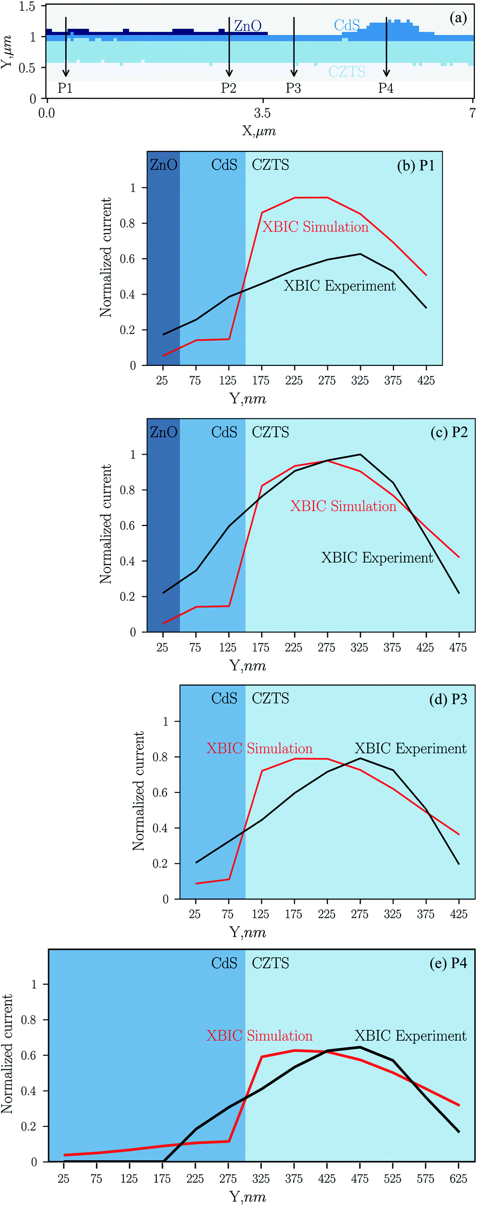 | ||
| Fig. 7 The computational domain (a) with the location of line profiles from the experimental and simulated data along P1, P2, P3 and P4 shown in (b–e). | ||
Fig. 7(b–e) present the line profiles from the experimental and simulation results along P1, P2, P3 and P4, respectively. From these figures, we can observe that the experimental XBIC peak is almost at the center of the absorber layer (CZTS), while in the simulation result, the XBIC peak is shifted towards the CZTS/CdS interface. In spite of this, we can see a good agreement between the experimental and simulation results in the absorber layer. In general, it is very hard to avoid the presence of the secondary phases in CZTS based solar cells,9 and the experimental peak shift might be due to the presence of such a phase near the heterointerface. Due to the experiment’s resolution limitations and 2D configuration it was difficult to deduce such a phase from the XRF data in our sample. Moreover, we can see a sharp loss of the charge collection (XBIC signal) in the simulation results near the heterointerface. One reason for this is the limited accuracy of the interface definition; construction of the domain from the XRF data is challenging due to the experimental resolution, and the spread of hot and thermalized charge carriers between the layers is not accounted for. Furthermore, a simple model at the heterointerface was used in our simulation considering the effective potentials for electrons and holes.
With the assumptions that ITO forms an ideal Schottky contact with the ZnO layer with a barrier height equal to 0.2 eV, and a barrier height equal to 0.5 eV at the CdS/ITO interface, we were able to simulate the effect of the absence of the ZnO layer on the right-hand side of the domain, as shown in Fig. 7(d). The results of Fig. 7(d and e) show that increasing the CdS thickness will increase the charge-carrier loss in the absorber layer.
In our simulation, we assumed homogeneous layers with constant parameters. From Fig. 7(b), we can see a lower current in the experimental result than in the simulation. This is related to the fact that P1 is lying in one of the regions with an inhomogeneous distribution of the absorber layer contents. We can see the correlation between the diffusion of Cd in the absorber layer and the XBIC signal highlighted by white arrows in Fig. 3.
5. Conclusions
Correlative scanning X-ray microscopy is a powerful tool for in situ and operando studies of functional materials such as solar cells, providing a spatially-resolved correlative characterization of the chemical composition and electrical performance at the nanoscale. From the analysis of the acquired data from different modalities, we see a significant potential of applying correlative scanning X-ray microscopy to new generations of solar cells. XRF maps allow us to visualize inhomogeneities in all the device layers and correlate them with local charge conversion efficiency obtained from XBIC measurements.The conventional approach of modeling the performance of solar cells considers the nominal architecture of the device. However, structural variations resulting, e.g., from the inhomogeneous deposition of layers during fabrication, as well as various defects occurring in real devices, are not considered. We present a framework in which the material parameters can be associated with the local electrical performance based on the actual structure of the device. The framework consists of constructing a computational domain from X-ray fluorescence data (and phase-contrast images, if needed) used for first-principles modeling of the XBIC signal. The model can then be used to interpret some aspects of the experimentally measured XBIC signal. Our approach shows that electronic defects can be identified by XBIC, correlated with compositional and structural inhomogeneities from XRF and phase contrast, and explained by simulations.
To address some limitations of the current implementation, new developments will be required, as the recorded data from a 2D projection of a micron-thick cross-section lamella does not allow the unambiguous assignment of chemical and morphological inhomogeneities on the scale of grains and grain boundaries. To achieve this, the data will have to be extended to 3D by tomographic acquisition and accompanying extension of the model to 3D. This is not trivial because of the added experimental complexity and because neither XRF or XBIC signals are simple line integrals of the beam path. However, it is feasible to mill out a pillar that is a functional solar cell48 and have it electrically connected during 3D scanning microscopy measurements.49,50 Algebraic iterative reconstruction algorithms may be applied to reconstruct the volumetric response of a non-linear beam–matter interaction.51,52 To realize a better representation of the typically nano-structured 3rd generation solar-cell devices, some more challenging requirements should ideally be met: the material properties need to be determined at the scale of the measurements and model, as they cannot be assumed to be representative of homogeneous materials. Furthermore, our simplistic approach includes Monte Carlo simulations for each material separately, which will necessarily lead to incorrect generation profiles at interfaces. We hope that these considerations will stimulate a constructive discussion on how to best overcome the challenges to make optimum use of the boosted brilliance of next-generation storage rings.53
Author contributions
Abdellatif Saadaldin: formal analysis, methodology, software, validation, visualization, writing – original draft, writing – review & editing. Azat M. Slyamov: investigation, methodology, validation, visualization, writing – original draft. Michael E. Stuckelberger: conceptualization, formal analysis, funding acquisition, investigation, methodology, project administration, supervision, validation, visualization, writing – original draft, writing – review & editing. Peter S. Jørgensen: investigation, methodology. Christian Rein: investigation. Mariana Mar Lucas: investigation. Tiago Ramos: investigation. Angel Rodriguez-Fernandez: investigation. Dominique Bernard: conceptualization, formal analysis, funding acquisition, methodology, project administration, supervision, validation, visualization, writing – original draft, writing – review & editing. Jens W. Andreasen: conceptualization, formal analysis, funding acquisition, investigation, methodology, project administration, supervision, validation, visualization, writing – original draft, writing – review & editing.Conflicts of interest
There are no conflicts to declare.Acknowledgements
The authors acknowledge the staff of NanoMAX, the hard X-ray nanoprobe beamline of the MAX IV synchrotron facility, for support with the multi-modal scanning nanoprobe experiment. Stela Canulescu, Sara Engberg, Andrea Crovetto, and Prof. Jørgen Schou are acknowledged for providing the investigated solar cell. This study was funded by EU Horizon 2020 Marie Skłodowska-Curie Actions Innovative Training Network: MUltiscale, Multimodal and Multidimensional imaging for EngineeRING (MUMMERING), grant no. 765604. The research leading to these results has received funding from Deutsches Elektronen-Synchrotron DESY.References
- P. A. Owusu and S. Asumadu-Sarkodie, A review of renewable energy sources, sustainability issues and climate change mitigation, Cogent Eng., 2016, 3(1), 1167990 CrossRef.
- M. Z. Jacobson and M. A. Delucchi, Providing all global energy with wind, water, and solar power, Part I: Technologies, energy resources, quantities and areas of infrastructure, and materials, Energy Policy, 2011, 39, 1154–1169 CrossRef CAS.
- M. A. Delucchi and M. Z. Jacobson, Providing all global energy with wind, water, and solar power, Part II: Reliability, system and transmission costs, and policies, Energy Policy, 2011, 39, 1170–1190 CrossRef.
- B. G. Gribov and K. V. Zinov’ev, Preparation of High-Purity Silicon for Solar Cells, 2003 Search PubMed.
- C. Battaglia, A. Cuevas and S. De Wolf, High-efficiency crystalline silicon solar cells: status and perspectives, Energy Environ. Sci., 2016, 9, 1552–1576 RSC.
- L. C. Andreani, A. Bozzola, P. Kowalczewski, M. Liscidini and L. Redorici, Silicon solar cells: toward the efficiency limits, Adv. Phys.: X, 2019, 4, 1548305 CAS.
- L. El Chaar, L. A. Lamont, and N. El Zein, Review of Photovoltaic Technologies, 2011 Search PubMed.
- M. Green, E. Dunlop, J. Hohl-Ebinger, M. Yoshita, N. Kopidakis and X. Hao, Solar cell efficiency tables (version 57), Prog. Photovolt., 2021, 29, 3–15 CrossRef.
- T. J. Huang, X. Yin, G. Qi and H. Gong, CZTS-based materials and interfaces and their effects on the performance of thin film solar cells, Phys. Status Solidi Rapid Res. Lett., 2014, 8, 735–762 CrossRef CAS.
- M. Kumar, A. Dubey, N. Adhikari, S. Venkatesan and Q. Qiao, Strategic review of secondary phases, defects and defect-complexes in kesterite CZTS–Se solar cells, Energy Environ. Sci., 2015, 8, 3134–3159 RSC.
- M. Stuckelberger, B. West, T. Nietzold, B. Lai, J. M. Maser, V. Rose and M. I. Bertoni, Review: Engineering solar cells based on correlative X-ray microscopy, J. Mater. Res., 2017, 32, 1825–1854 CrossRef CAS.
- M. E. Stuckelberger, T. Nietzold, B. West, R. Farshchi, D. Poplavskyy, J. Bailey, B. Lai, J. M. Maser and M. I. Bertoni, Defect activation and annihilation in CIGS solar cells: an operando x-ray microscopy study, JPhys Energy, 2020, 2, 25001 CrossRef CAS.
- R. P. Winarski, M. V. Holt, V. Rose, P. Fuesz, D. Carbaugh, C. Benson, D. Shu, D. Kline, G. Brian Stephenson, I. McNulty and J. Maser, A hard X-ray nanoprobe beamline for nanoscale microscopy, J. Synchrotron Radiat., 2012, 19, 1056–1060 CrossRef CAS PubMed.
- U. Johansson, U. Vogt, and A. Mikkelsen, NanoMAX: a hard X-ray nanoprobe beamline at MAX IV, in X-Ray Nanoimaging: Instruments and Methods, International Society for Optics and Photonics, 2013, vol. 8851, p. 88510L Search PubMed.
- G. Martínez-Criado, J. Villanova, R. Tucoulou, D. Salomon, J.-P. Suuronen, S. Labouré, C. Guilloud, V. Valls, R. Barrett and E. Gagliardini, et al., ID16B: a hard X-ray nanoprobe beamline at the ESRF for nano-analysis, J. Synchrotron Radiat., 2016, 23, 344–352 CrossRef PubMed.
- A. Schropp, R. Döhrmann, S. Botta, D. Brückner, M. Kahnt, M. Lyubomirskiy, C. Ossig, M. Scholz, M. Seyrich and M. E. Stuckelberger, et al., PtyNAMi: ptychographic nano-analytical microscope, J. Appl. Crystallogr., 2020, 53, 957–971 CrossRef CAS PubMed.
- M. Trushin, O. Vyvenko, W. Seifert, M. Kittler, I. Zizak, A. Erko, M. Seibt and C. Rudolf, Combined XBIC/μ-XRF/μ-XAS/DLTS investigation of chemical character and electrical properties of Cu and Ni precipitates in silicon, Phys. Status SolidiC, 2009, 6, 1868–1873 CrossRef CAS.
- C. Ossig, T. Nietzold, B. West, M. Bertoni, G. Falkenberg, C. G. Schroer and M. E. Stuckelberger, X-ray Beam Induced Current Measurements for Multi-Modal X-ray Microscopy of Solar Cells, J. Visualized Exp., 2019, 2019, e60001 Search PubMed.
- A. Ulvestad, S. O. Hruszkewycz, M. V. Holt, M. O. Hill, I. Calvo-Almazán, S. Maddali, X. Huang, H. Yan, E. Nazaretski, Y. S. Chu, L. J. Lauhon, N. Rodkey, M. I. Bertoni and M. E. Stuckelberger, Multimodal x-ray imaging of grain-level properties and performance in a polycrystalline solar cell, J. Synchrotron Radiat., 2019, 26, 1316–1321 CrossRef CAS PubMed.
- I. Calvo-Almazán, A. P. Ulvestad, E. Colegrove, T. Ablekim, M. V. Holt, M. O. Hill, S. Maddali, L. J. Lauhon, M. I. Bertoni, X. Huang, H. Yan, E. Nazaretski, Y. S. Chu, S. O. Hruszkewycz and M. E. Stuckelberger, Strain mapping of CdTe grains in photovoltaic devices, IEEE J. Photovolt., 2019, 9, 1790–1799 Search PubMed.
- C. Ossig, C. Strelow, J. Flügge, A. Kolditz, J. Siebels, J. Garrevoet, K. Spiers, M. Seyrich, D. Brückner, N. Pyrlik, J. Hagemann, F. Seiboth, A. Schropp, R. Carron, G. Falkenberg, A. Mews, C. G. Schroer, T. Kipp and M. E. Stuckelberger, Four-fold multi-modal X-ray microscopy measurements of a Cu(In,Ga)Se2 solar cell, Materials, 2021, 14, 228 CrossRef CAS PubMed.
- G. Falkenberg, J. Hense, J. Barp, C. Ossig, N. Pyrlik, C. Ziska, M. Seyrich, J. Hagemann, M. Lyubomirskiy, F. Seiboth, G. Fevola, S. Patjens, J. Garrevoet, G. Falkenberg and M. E. Stuckelberger, Comparison of XBIC and LBIC measurements of a fully encapsulated c-Si solar cell, in 2021 48th IEEE Photovoltaic Specialists Conference (PVSC), 2021, pp. 1998–2004 Search PubMed.
- L. Chayanun, G. Otnes, A. Troian, S. Hammarberg, D. Salomon, M. T. Borgström and J. Wallentin, Nanoscale mapping of carrier collection in single nanowire solar cells using X-ray beam induced current, J. Synchrotron Radiat., 2019, 26, 102–108 CrossRef CAS PubMed.
- N. M. Kumar, A. R. Shaik, T. Walker, T. Nietzold, B. Lai, E. Colegrove, M. Stuckelberger, and M. Bertoni, Mapping current collection in cross section: The case of copper-doped CdTe solar cells, in 2020 47th IEEE Photovoltaic Specialists Conference, PVSC, 2020, pp. 2178–2180 Search PubMed.
- T. Walker, M. E. Stuckelberger, T. Nietzold, N. Mohan-Kumar, C. Ossig, M. Kahnt, F. Wittwer, B. Lai, D. S. E. Colegrove and M. I. Bertoni, The nanoscale distribution of copper and its influence on charge collection in CdTe solar cells, Nano Energy, 2022, 91, 106595 CrossRef CAS.
- A. Cazzaniga, A. Crovetto, C. Yan, K. Sun, X. Hao, J. Ramis Estelrich, S. Canulescu, E. Stamate, N. Pryds, O. Hansen and J. Schou, Ultra-thin Cu2ZnSnS4 solar cell by pulsed laser deposition, Sol. Energy Mater. Sol. Cells, 2017, 166, 91–99 CrossRef CAS.
- M. Stuckelberger, B. West, S. Husein, H. Guthrey, M. Al-Jassim, R. Chakraborty, T. Buonassisi, J. M. Maser, B. Lai, B. Stripe, V. Rose, and M. Bertoni, Latest developments in the x-ray based characterization of thin-film solar cells, 42nd IEEE Photovoltaic Specialists Conference (PVSC), 2015, pp. 1–6 Search PubMed.
- G. Fevola, P. S. Jørgensen, M. Verezhak, A. Slyamov, A. Crovetto, Z. I. Balogh, C. Rein, S. Canulescu and J. W. Andreasen, Resonant X-ray ptychographic nanotomography of kesterite solar cells, Phys. Rev. Res., 2020, 2, 013378 CrossRef CAS.
- M. M. Lucas, T. Ramos, P. S. Jørgensen, S. Canulescu, P. Kenesei, J. Wright, H. F. Poulsen and J. W. Andreasen, Non-destructive determination of phase, size, and strain of individual grains in polycrystalline photovoltaic materials, J. Alloys Compd., 2021, 887, 161364 CrossRef.
- A. Menzel, C. M. Kewish, P. Kraft, B. Henrich, K. Jefimovs, J. Vila-Comamala, C. David, M. Dierolf, P. Thibault, F. Pfeiffer and O. Bunk, Scanning transmission X-ray microscopy with a fast framing pixel detector, Ultramicroscopy, 2010, 110, 1143–1147 CrossRef CAS PubMed.
- C. Ziska, C. Ossig, N. Pyrlik, R. Carron, E. Avancini, G. Fevola, A. Kolditz, J. Siebels, T. Kipp, Z. Cai, et al., Quantifying the elemental distribution in solar cells from x-ray fluorescence measurements with multiple detector modules, in 2020 47th IEEE Photovoltaic Specialists Conference (PVSC), 2020, pp. 1085–1092 Search PubMed.
- O. Vyvenko, T. Buonassisi, A. Istratov, H. Hieslmair, A. Thompson, R. Schindler and E. Weber, X-ray beam induced current—a synchrotron radiation based technique for the in situ analysis of recombination properties and chemical nature of metal clusters in silicon, J. Appl. Phys., 2002, 91, 3614–3617 CrossRef CAS.
- T. Buonassisi, M. Heuer, O. Vyvenko, A. Istratov, E. Weber, Z. Cai, B. Lai, T. Ciszek and R. Schindler, Applications of synchrotron radiation x-ray techniques on the analysis of the behavior of transition metals in solar cells and single-crystalline silicon with extended defects, Phys. B, 2003, 340–342, 1137–1141 CrossRef CAS.
- F. Salvat, J. M. Fernández-Varea, and J. Sempau, PENELOPE-2006: A code system for Monte Carlo simulation of electron and photon transport, in Workshop Proceedings, Nuclear Energy Agency, Organization for Economic Co-operation and Development, 2006, vol. 4 Search PubMed.
- J. A. Nelson, The Physics of Solar Cells, World Scientific Publishing Company, 2003 Search PubMed.
- D. Scharfetter and H. Gummel, Large-signal analysis of a silicon Read diode oscillator, IEEE Trans. Electron Devices, 1969, 16, 64–77 Search PubMed.
- H. K. Gummel, A self-consistent iterative scheme for one-dimensional steady state transistor calculations, IEEE Trans. Electron Devices, 1964, 11, 455–465 Search PubMed.
- J. B. Ghasemi, M. K. Rofouei and N. Amiri, Multivariate curve resolution alternating least squares in the quantitative determination of sulfur using overlapped S(Kα)-Mo(Lα) emission peaks by wavelength dispersive X-ray fluorescence spectrometry, X-Ray Spectrom., 2015, 44, 75–80 CrossRef CAS.
- A. O. M. Alzahrani, M. S. Abdel-wahab, M. Alayash and M. S. Aida, Metals and ITO contact nature on ZnO and NiO thin films, Braz. J. Phys., 2021, 51, 1159–1165 CrossRef CAS.
- D. Cozza, C. M. Ruiz, D. Duche, J. J. Simon and L. Escoubas, Modeling the back contact of Cu2ZnSnSe4 solar cells, IEEE J. Photovolt., 2016, 6, 1292–1297 Search PubMed.
- A. Crovetto, M. L. Palsgaard, T. Gunst, T. Markussen, K. Stokbro, M. Brandbyge and O. Hansen, Interface band gap narrowing behind open circuit voltage losses in Cu2ZnSnS4 solar cells, Appl. Phys. Lett., 2017, 110, 083903 CrossRef ..
- A. Cherouana and R. Labbani, Study of CZTS and CZTSSe solar cells for buffer layers selection, Appl. Surf. Sci., 2017, 424, 251–255 CrossRef CAS.
- A. Benmir and M. S. Aida, Simulation of a thin film solar cell based on copper zinc tin sulfo-selenide Cu2ZnSn(S,Se)4, Superlattices Microstruct., 2016, 91, 70–77 CrossRef CAS.
- A. Kumar and A. D. Thakur, Role of contact work function, back surface field, and conduction band offset in Cu2ZnSnS4 solar cell, Jpn. J. Appl. Phys., 2018, 57, 08RC05 CrossRef.
- I. M. Dharmadasa, Recent developments and progress on electrical contacts to CdTe, CdS and ZnSe with special reference to BARRIER contacts to CdTe, Prog. Cryst. Growth Charact. Mater., 1998, 36, 249–290 CrossRef CAS.
- S. Choi, Z. Shaolin and W. Yang, Layer-number-dependent work function of MoS2 nanoflakes, J. Korean Phys. Soc., 2014, 64, 1550–1555 CrossRef CAS.
- A. R. Latrous, R. Mahamdi, B. N. Touafek and M. Pasquinelli, Performance enhancement in CZTS solar cells by SCAPS-1D software, Int. J. Thin Film Sci. Technol., 2021, 10, 59–65 CrossRef.
- H. F. Dam, T. R. Andersen, E. B. L. Pedersen, K. T. S. Thydén, M. Helgesen, J. E. Carlé, P. S. Jørgensen, J. Reinhardt, R. R. Søndergaard, M. Jørgensen, E. Bundgaard, F. C. Krebs and J. W. Andreasen, Enabling flexible polymer tandem solar cells by 3D ptychographic imaging, Adv. Energy Mater., 2015, 5, 1400736 CrossRef.
- P. Parkinson, Y.-H. Lee, L. Fu, S. Breuer, H. H. Tan and C. Jagadish, Three-dimensional in situ photocurrent mapping for nanowire photovoltaics, Nano Lett., 2013, 13, 1405–1409 CrossRef CAS PubMed.
- L. Chayanun, L. Hrachowina, A. Björling, M. T. Borgström and J. Wallentin, Direct three-dimensional imaging of an x-ray nanofocus using a single 60 nm diameter nanowire device, Nano Lett., 2020, 20, 8326–8331 CrossRef CAS PubMed.
- K. W. Bossers, R. Valadian, S. Zanoni, R. Smeets, N. Friederichs, J. Garrevoet, F. Meirer and B. M. Weckhuysen, Correlated x-ray ptychography and fluorescence nano-tomography on the fragmentation behavior of an individual catalyst particle during the early stages of olefin polymerization, J. Am. Chem. Soc., 2020, 142, 3691–3695 CrossRef CAS PubMed.
- J. Becher, D. F. Sanchez, D. E. Doronkin, D. Zengel, D. M. Meira, S. Pascarelli, J.-D. Grunwaldt and T. L. Sheppard, Chemical gradients in automotive Cu-SSZ-13 catalysts for NOx removal revealed by operando x-ray spectrotomography, Nat. Catal., 2021, 4, 46–53 CrossRef CAS.
- M. E. Stuckelberger, Multimodal scanning x-ray microscopy at nanoprobe endstations of fourth-generation synchrotrons, Spectroscopy, 2019, 34, 42–44 Search PubMed.
Footnote |
| † These two authors contributed equally. |
| This journal is © The Royal Society of Chemistry 2022 |