
 Open Access Article
 This Open Access Article is licensed under a Creative Commons Attribution-Non Commercial 3.0 Unported Licence
Single molecule electronic devices with carbon-based materials: status and opportunity
Shima
Ghasemi
and
Kasper
Moth-Poulsen
 *
*
Department of Chemistry and Chemical Engineering, Chalmers University of Technology, SE-412-96 Göteborg, Sweden. E-mail: kasper.moth-poulsen@chalmers.se
First published on 18th December 2020
Abstract
The field of single molecule electronics has progressed remarkably in the past decades by allowing for more versatile molecular functions and improving device fabrication techniques. In particular, electrodes made from carbon-based materials such as graphene and carbon nanotubes (CNTs) may enable parallel fabrication of multiple single molecule devices. In this perspective, we review the recent progress in the field of single molecule electronics, with a focus on devices that utilizes carbon-based electrodes. The paper is structured in three main sections: (i) controlling the molecule/graphene electrode interface using covalent and non-covalent approaches, (ii) using CNTs as electrodes for fabricating single molecule devices, and (iii) a discussion of possible future directions employing new or emerging 2D materials.
Introduction
Semiconductor technology is ubiquitous in our modern, connected society. In recent years, the use of on-line devices powering the internet of things (IoT) has massively expanded. This transformation is powered by impressive developments in the fabrication and miniaturization of silicon-based systems. Yet, to realize the rapid miniaturization trend as described by Moore's law will likely require new technologies.1 These technologies should not only be quantum sized, but also consume little power, have a low environmental ramification and must be competitive in terms of cost. In this context, single-molecule electronics have been explored for several decades as one possible avenue for electronic devices. For example, single molecule devices with advanced functions such as switching,2–4 rectification,5,6 transistors7,8 and molecular diodes9 have been developed. However, parallel fabrication and reproducibility remain key issues for single-molecule electronic devices.This could be resolved using carbon-based materials. In particular, graphene significantly reduces the number of possible contact geometries and adds compelling electronic functions to single-molecule electronic devices. 2D materials may soon also enable parallel fabrication of single-molecule electronic devices for the first time. In this review, we highlight and discuss the status and opportunities of carbon-based materials used in single-molecule electronics devices focusing on the progress in the recent 3–5 years (2016–2020). This review concentrates on devices with a single or a small number of active molecules. The broader field of electronic devices based on self-assembled monolayers (SAMs) is not within the scope of this review.10–12,13
Molecule-electrode interface
When working with single molecule electronics devices, the gold coupled organic molecules with thiol based “alligator clips” have been the preferred electrodes. However, the high atomic mobility and low chemical stability of metallic contacts could induce the destruction of molecular junctions upon oxidation or electromigration. Furthermore, small variations in the positioning of a single molecule onto the electrode may radically affect the electronic coupling between the molecule and electrode. Further, the positioning of a gate close to the molecule in the metallic nanogap is difficult. These challenges could limit practical device function.14–17 Therefore, controlling the fabrication of molecular junctions in the electrode–molecule interface has been challenging. Using electrodes made of graphene could be a viable solution for the formation of reliable molecular junctions. Arrangement of sp2-hybridized carbon atoms in graphene provides the desired compatibility with organic molecules. The 2D structure of graphene reduces the number of possible contact geometries compared to 3D structures, which potentially leads to a more reproducible single molecule device. The binding of anchoring groups to graphene electrodes can be achieved by either π–π interaction or covalent bonding. Anchoring groups play a crucial role for improving the mechanical stability and electronic coupling of the molecule–electrode interface when they are attached to the molecular backbone. Other factors such as inserting spacers between the molecular backbone and anchoring groups could optimize the molecule–electrode interface efficiently. With this review, we present how different anchoring groups can control charge transport properties, switches and facilitate dynamic investigations based on the graphene–molecule–graphene single-molecule junctions (GMG-SMJs).Non-covalent bonding between molecule and graphene electrode
Interaction of different anchoring groups with electrodes can directly influence the charge transport behavior of single-molecule devices. Any change of the molecular electrode interface, either electronically or geometrically could significantly change the electrical conductance (G) of single molecules. In order to control the molecule–electrode interface through π–π stacking with a number of different anchoring groups (Fig. 1, structure a–i) has been investigated. In particular, El Abbassi et al. obtained a mechanically stable device by anchoring a small number of molecules onto the SiO2 substrate between two graphene electrodes through a silanization reaction.18 The molecule was comprised of three main parts: a silane group, a π-conjugated head group and a non-conjugated alkane chain (Fig. 2a). The silane group facilitated the chemical anchoring of the molecule to the substrate via covalent bonding. This covalent anchoring of the molecule to the substrate overcame the problem of ill-defined edge terminations in graphene that can occur after nanofabrication or preparation of the contact electrodes. Additionally, covalent bonds between the molecule and the substrate led to stable graphene–molecule junctions. The π-conjugated head group biphenyl N-carbazole (BPC; Fig. 1a) ensured coupling to graphene through π–π interaction. The non-conjugated alkane chain decoupled the mechanical anchoring from the electronic head group. To reveal the transport characteristics at the molecule–electrode interface in the device, density functional theory (DFT) calculations have been performed. DFT analysis indicated that the frontier orbitals of the BPC molecule were mostly localized on the head group. This shows that the electron transport occurs mainly through the head group. They also found the evidence for the formation of transport channels between the head groups of two neighboring molecules through π–π stacking in the graphene nanogap (Fig. 2b). Apart from the BPC molecule, they did electrical characterization of devices with other headgroups, i.e., molecule C with a carbazole (Fig. 1b) and molecule M without a π-conjugated head group. Current–voltage (I–V) curves showed a maximum current of about 10 picoampere (pA) at a bias voltage (Vb) of 2 V for the junction using molecule M. I–V curves for the junctions using molecule C illustrated efficient charge transport over the molecular junction through π–π stacking. The alteration in I–V shapes and current levels were explained by the weak electronic interaction between the neighboring head groups, which were arranged in various molecular conformations.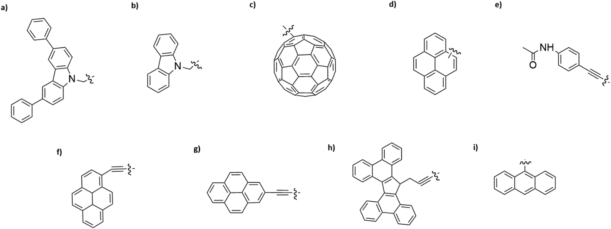 | ||
| Fig. 1 Examples of non-covalent anchoring groups used in graphene-based devices. (a) Biphenyl N-carbazole, (b) Carbazole, (c) Fullerene, (d) Pyrene, (e) Amine, (f) Pyrene-1, (g) Pyrene-2, (h) Tetrabenzofluorene, (i) Anthracene. | ||
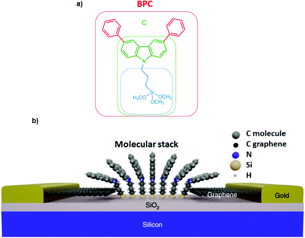 | ||
| Fig. 2 (a) Molecular structure. (b) Schematic of the molecular junction including molecules bridged via different π–π-stacking into graphene. Reprinted with permission from El Abbassi et al., Nat. Nanotechnol., 2019, 14, 957. Copyright 2019 Nature Publishing Group. | ||
Tan et al. realized a different approach for investigation of charge transport through a class of junctions using the mechanically controlled break junction (MCBJ) technique.19 They fabricated single-fullerene (Fig. 1c) junctions with a fullerene bridged between two graphene electrodes via van der Waals interactions. A one-dimensional (1D) conductance histogram of graphene/single-C60, C70, C76, C90/graphene junctions indicated that the conductance improved >250% from 2.0 × 10⁻⁵G0 to 5.1 × 10⁻⁵G0 when the size of the fullerene was changed from C60 to C90. Furthermore, they observed that the conductance was enhanced after the fullerene was doped with a nitrogen atom. For example, the conductance of graphene/single-(C59N)2/graphene increased by 150% reaching 2.1 × 10⁻⁵G0 compared to the conductance of graphene/single-C120/graphene junctions. However, when breaking the conjugation of the π-system of fullerene, the conductance decreased. The conductance of low-conjugated graphene/single-C50H10/graphene junctions decreased by about one order of magnitude compared to the conductance of conjugated single-C60.
The charge transport in a series of C60-graphene junctions has been investigated by Leitherer et al. using DFT and Landauer transport theory.20 As building blocks of the molecular junctions, they used a molecular bridge between two C60 molecules connected by two styrene groups covalently attached to the [2,2] paracyclophane moiety in the center of C60. The two fullerene anchor groups of this structure were bound to graphene electrodes through π–π interaction.21 They found out two structural conformers with either zigzag- or armchair-terminated graphene nanocontacts (Fig. 3a and b) and investigated how electronic transport is influenced by graphene edge terminations. Interestingly, the edge-induced transport contributions were only observed in conformer A with zigzag-terminated graphene electrodes. This phenomenon was explained by the differences in the interface geometry and the resulting molecule–graphene contact in conformer A. As it is shown in Fig. 3, for conformer B dimer/bridge and a hexagon hole geometry corresponded to the left- and right-hand side respectively. The binding energy of the hexagon/hole and pentagon/hole orientation, corresponded to conformer A, was higher than that of the dimer/bridge geometry, which resulted the lower molecule–electrode coupling in conformer B. The different coupling strengths in the pentagon and hexagon geometries was corroborated by earlier experimental work by Danilov et al.22 who studied voltage-induced switching in single C60 molecules located in the nano gap between two silver electrodes.
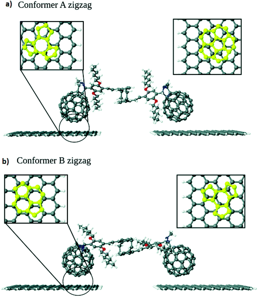 | ||
| Fig. 3 Interface geometry of (a) conformer A and (b) conformer B. Reprinted with permission from Leitherer et al., Nanoscale, 2017, 9, 7217. Copyright 2017 Royal Society of Chemistry. | ||
Limburg et al. explored five derivatives of zinc porphyrin in single-molecule junctions to find out the effect of various non-covalent anchor groups on charge transport properties and the junction formation probability (JFP).23 The five derivatives were constituted of an identical redox-active zinc porphyrin core and different flat π-aromatic systems as anchor groups. They chose one reference molecule without anchor groups. Tetrabenzofluorene (Fig. 1h) anchors showed different charge transport behaviour compared to the other anchors as they are not π-conjugated with the porphyrin. The JFP is highly depended on the anchor group. The larger anchor groups indicated higher binding energy which corresponded with higher JFPs of molecular devices. Specially, in this experiment, they showed that larger anchor groups had a significant positive effect on JFP. For example, 1,3,8-tridodecyloxypyrene and 2,5,8,11,14-pentadodecylhexa-peri hexabenzocoronene had the highest JFPs values of about 36% and 38%, respectively. They also showed that additional alkyl tails on the π-systems played the role for better interaction of the π-system to the graphene. The large binding energies and high JFP of lager anchor groups make them as a potential candidate for fabrication of devices based on molecular anchoring to graphene via π-stacking.
To investigate electron transport through spin-crossover (SCO) molecules at the single molecular level, Burzurí et al. bridged the molecule [Fe(L)2] (BF4)2·CH3CN·H2O (Fe-SCO) between two few-layer graphene (FLG) electrodes.24 The coordination of two 2,6-bispyrazolylpyridine (bpp) ligands (L) with Fe(II) was through an octahedral (Oh) symmetry distorted to a S4 symmetry. Two pyrene (Fig. 1d) groups anchored these ligands via π–π stacking to graphene electrodes. After deposition of the Fe-SCO molecules, they calculated the current (I)–voltage (V) characteristics at cryogenic temperatures for three different junctions containing an Fe-SCO molecule. When a molecular junction was formed, the current was increased sharply around two orders of magnitude compared with the empty junction. In these three junctions, they observed a reproducible conductance bi-stability between a large-gap (LG) and a small-gap (SG) state. This observation confirmed that the spin-crossover switch was active in these single-molecule junctions. DFT analysis indicated that the SCO transition induced a considerable change in the energy spectrum of the molecular orbitals led to conductance bistability. It has been shown that small changes of the ligand distance in the molecular junctions could induce switching between high-spin (HS) and low-spin (LS) states at the single-molecule level at any temperature. Lau et al. studied the charge transport properties across a graphene–fullerene single-molecule transistor using a C60 bisadduct functionalized with pyrene as an anchoring group. Two pyrene anchor groups were bound to graphene nanoelectrodes via π–π interactions.25 DFT calculations revealed that the most stable configuration was the cis-3 isomer of relaxed graphene–fullerene–graphene structure without steric hindrance. The iso-surfaces of the frontier orbitals for cis-3 and cis-2 indicated that the cis-3 isomer showed better π–π interaction with the graphene electrodes. It should be noted that the transport in pristine C60 was dominated by the lowest unoccupied molecular orbital (LUMO), whereas functionalization of C60 with pyrene anchoring groups modified the electron delocalization and energy levels, which led to transport dominated by the highest occupied molecular orbital (HOMO). Due to the stability of the device which showed weak vibron-relaxation, they investigated redox-dependent electron–vibron coupling and avalanche transport.
To identify the influence of different anchoring groups on the transport through graphene-based molecular junctions, Sadeghi et al. theoretically determined the electronic properties of zinc-porphyrin monomers, dimers, and trimers attached to graphene electrodes through either π–π or covalent anchoring.26 The authors’ model device structure was comprised of monomer, dimer and, trimer zinc-porphyrin wires coupled to graphene electrodes (Fig. 4a) through either covalent C–C bond attachment to the edge of the graphene ribbons (Fig. 4b), amine anchors (Fig. 4c), π–π stacking through pyrene with two different moieties (Fig. 4d and e) or a tetrabenzofluorene (TBF) anchoring group (Fig. 4f). Direct C–C coupling was found to have the highest conductance, followed by π–π stacking with the pyrene anchors, direct coupling via amine anchors, and π–π stacking with TBF. The direct C–C bonds were coupled to the electrodes more strongly than other anchoring groups because of the great width of the HOMO resonance in this junction.27 Depending on the connectivity of the pyrene anchor groups to the porphyrin wire, pyrene anchors could induce either destructive quantum interference or different degrees of constructive quantum interference. However, the coupling of TBF to both the graphene and the porphyrin wires were weak as the twisted structure of the TBF anchors provided a nonuniform π–π overlap between π-orbitals of TBF and the graphene electrodes. Furthermore, the disturbance in the conjugation of the π-aromatic system at the cyclopentadiene connection point led to a reduction in the conductance and electronic coupling. The lower conductance of amine anchors was explained by presence of a carbonyl group, which broke the conjugation of the π-aromatic system.
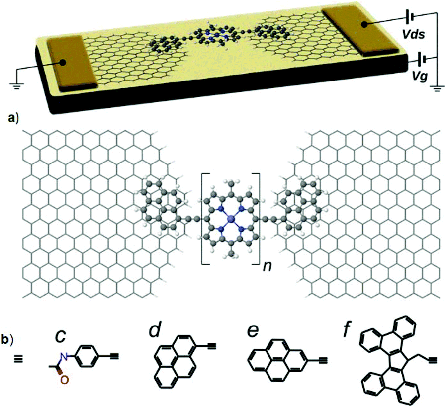 | ||
| Fig. 4 (a) The porphyrin wires with one, two, and three zinc porphyrin units (n = 1, 2, 3) are contacted to the graphene by pyrene anchors. Other anchor groups studied include covalent anchoring to the edge of graphene electrodes via (b) a direct carbon–carbon bond and (c) amine anchors or through π–π interactions with (d) pyrene-1 anchors, (e) pyrene-2 anchors, and (f) tetrabenzofluorene (TBF) anchors. Reprinted with permission from Sadeghi et al., Nano Lett., 2017, 17, 4611. Copyright 2017 American Chemical Society. | ||
Prins et al. developed a method for the formation of nanometer-separated FLG electrodes by using the feedback-controlled electroburning technique.28 The high stability of these electrodes was demonstrated by only small variations in the tunneling characteristics after several weeks of storage under vacuum condition. In order to show the long-term stability and gate independent transport across the gap, an anthracene-functionalized curcuminoid molecule (1,7-(di-9-anthracene)-1,6-heptadiene-3,5-dione, 9Accm) was placed in the graphene nanogap. The anthracene groups (Fig. 1i) interacted via π–π interactions with the FLG electrodes and the high π-electron density of 9 Accm facilitated the charge transport. The difference in I–V characteristics before and after molecule deposition could be explained by the presence of molecules in the gap influencing its stability. Before deposition, the conductance was gate-independent and after deposition, the conductance of the device improved and gate-dependent transport at room temperature was observed, indicative of molecular device formation.
A more reproducible electrode–molecule contact than for traditional anchoring groups covalently binding to the metal electrode has been achieved by designing a new curcuminoid-based molecule (9ALCccmoid) with a well-defined geometry of aromatic anchoring groups such as pyrene and anthracene.29 9ALCccmoid was comprised of a conjugated linear chain of 11 C atoms which included a β-diketone group at the center of the backbone and two anthracene groups situated on both sides of the chain. The molecule–electrode interface was controlled by π–π stacking of the anthracene groups to the FLG electrodes. I–V curves revealed that the current was reduced during controlled electroburning of a typical device in each step. Modelling of the structure indicated that the 9ALCccmoid molecule was positioned on top of the vicinity of each graphene electrode with one anthracene group. An energy minimum observed with a negligible relative horizontal shift of the graphene electrodes could be the reason for the nonsymmetric final structure.
The charge transport through a stable single-molecule single-electron transistor (SET) was investigated by Mol et al.30 They used a molecular backbone of a zinc-porphyrin moiety connecting to ‘butterfly’ TBF anchoring groups with a spacer, which facilitated the binding via π–π-stacking to defect free graphene nano-electrodes. DFT analysis revealed no sign of steric hindrance to adsorption as well as a planar geometry of the molecular wire across the graphene nanogap. A wide range of molecular wires can possibly be used for the π–π anchoring to the highly stable graphene electrodes.
Covalent bonding between molecule and graphene electrodes
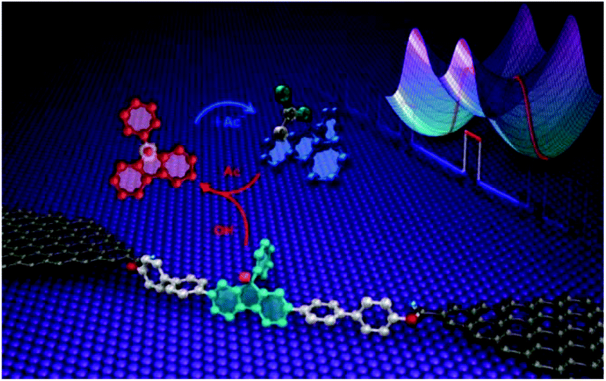
Apart from studying the charge transport properties within single molecule electronics, there are several reports using GMG-SMJ platform for investigation of dynamic processes at the single-molecule level such as host–guest interactions, hydrogen bond interactions, and intermolecular chemical reactions. In these studies, they controlled the molecule–electrode interface by covalent coupling of a wide range of organic molecules have been used with graphene electrodes.Using of single-molecule junctions for studying reaction mechanism at the single-event level has been recently reported. Gu et al. developed a method to use single-molecule junctions (SMJs) as an electrical platform to measure a reversible unimolecular nucleophilic substitution (SN1) reaction at the single-molecule level.31 Stable graphene–molecule–graphene single-molecule junctions (GMG-SMJs) were formed via covalent attachment of a single molecular wire comprised of a functional center of 9-phenyl-9-fluorenol into graphene nano-gapped electrodes (Fig. 5). To determine the acid-catalyzed SN1 reaction mechanism, the authors applied 9-phenyl-9-fluorenol as a reactant in the mixture of acetic acid (HAc) and trifluoroacetic acid (TFA). They found that the reaction proceeded in two steps. First, when the leaving group departed from the reactant, the carbocation formed an intermediate. Then, a nucleophile attached to the carbocation intermediate to form the final product. The acidic environment was assumed to stabilize the carbocation intermediate. For further investigation of reaction mechanism, competitive reactions between different nucleophiles were performed. In consistent with this, they studied the role of bromide anion in solution as another nucleophile. After monitoring reactions between the carbocation and different nucleophiles, the authors found different rate constants for the heterolytic dissociation process of the acetate/bromide forms (kd) and the combination process of the carbocation with acetic acid and bromide (kc). After comparing the reaction condition without the addition of the bromide anion, the authors confirmed that carbocation was an inevitable intermediate in the transition between the bromide and acetate forms, indicative of a classical SN1 mechanism. The authors were able to distinguish the carbocation electrically from the reactant and product because the conductance increased when the hybridization was changed from sp3 to sp2.
 | ||
| Fig. 5 Schematic of a graphene–molecule–graphene single-molecule junction which indicates the formation dynamics of a 9-phenyl-9-fluorenyl cation in an SN1 reaction. Reprinted with permission from Gu et al., Nano Lett., 2018, 18, 4156. Copyright 2018 American Chemical Society. | ||
To investigate the dynamic process of basic chemical reactions, Guan et al. also took advantage of GMG-SMJs.32 The authors investigated the reaction dynamics between carbonyl groups on GMG-SMJs and NH2OH in solution using a microchannel, in which the solution was confined to a small channel area. They were able to observe a base-catalyzed nucleophilic addition reaction between the carbonyl group on the molecule and NH2OH in solution. After the loss of an H2O molecule from the intermediate, oxime was formed as a final product. The junctions were constructed via covalent bonding of a single molecule with 9-fluorenone in the center to graphene electrodes. The authors suggested that the noticeable stability of the GMG-SMJs was owing to the formation of amide linkages by covalent coupling of amino groups to graphene electrodes. To gain more insight into the formation of the GMG-SMJs, I–V curves of the devices were recorded. The current was observed to decrease after etching by oxygen plasma. However, the recovery of the current after molecular assembly indicated successful device fabrication. Computationally calculated reaction energy profiles indicated the transformation of a reactant state (RS) to a shallow intermediate (IS′), and subsequently, to a stable intermediate state (IS) through proton transfer in water. Although a few microseconds were required for the reversible reaction from RS to IS, the reverse reaction from the final product state (PS) to IS took thousands of hours. Hence, high- and low-conductance states with dwell times of a few microseconds corresponded to the reversible reaction between the RS and IS.
To investigate hydrogen bond dynamics at the molecular level, Zhou et al. constructed hydrogen bond-bridged SMJs (HBB-SMJs) using promising strategy in which a ureido pyrimidine-dione (UPy) monomer molecule was covalently coupled between graphene point contacts.33 A UPy molecule can easily dimerize in a weak polar solvent such as diphenyl ether. In this study, A UPy dimer played the role as a good conducting channel and facilitated the formation of a strong donor–donor–acceptor–acceptor array of intermolecular quadruple hydrogen bonding. However, changing to strong polar solvents such as water, diphenyl ether could lead to on–off switching of the conductance of HBB-SMJs. This result indicated the successful fabrication of the devices. After studying the obtained current–time (I–t) curves in 1,1,2,2-tetrachloroethane (TeCA) at 293 K, they observed a series of large-amplitude two-state fluctuations with considerable dependency to temperature and solvent dependence. It has been shown that compared to the ‘high’ state conductance, the conductance of the ‘low’ state was much smaller which indicated a weaker hydrogen bonding system. The average lifetimes for the high-conductance and low-conductance states were reported τhigh = ∼0.660 ± 0.042 ms and τlow = ∼0.581 ± 0.042 ms respectively. In order to clarify the dynamic mechanism, they studied the experiments in two solvents with three different temperatures. They observed two large-amplitude peaks in TeCA. However, a multimodal distribution (at least four obvious peaks) was detected in diphenyl ether suggesting different mechanisms of intermolecular interactions through hydrogen bonding in different solvents. Both experimental and theoretical results revealed that a multimodal distribution could arise from the stochastic rearrangement of the hydrogen bond structure mainly through intermolecular proton transfer and lactam–lactim tautomerism. This work shows a promising strategy for investigation of hydrogen bond dynamics at the single molecule level.
To study the capability of particular GMG-SMJs to discover thermodynamic and kinetic parameters of a host–guest complex, Wen et al. constructed a conjugated molecular wire featuring bis-p-phenylene [34] crown-10 (BPP34C10) terminated with two amine handles namely, BPP34C10DAM that was covalently attached to carboxylic acid–terminated graphene point contacts using a 1-ethyl-3-(3-dimethylaminopropyl)carbodiimide (EDCI) coupling protocol.34 With this interface, they were able to transduce the physical pseudorotaxane (de)formation processes between the electron-rich crown ether and a dicationic guest into real-time electrical signals. To gain more insight to the influence of host–guest interactions on the conductivity of molecular junctions, they started the complexation by introducing methyl viologen (MV2+), which widely used as a guest for the BPP34C10 host, into the GMG-SMJ system. After immersion in a Me2SO solution containing 1 mM MV·2PF6 for 12 hours. The I–t curves of resulting devices (MV2+ ⊂ BPP34C10-SMJs) indicated two distinct “high” and “low” states. With the knowledge of a change in conductance in the solid state after MV2+ addition, the high and low conductance sates could be attributed to the association and dissociation processes between the BPP34C10 host and MV2+ guest molecules at the device-liquid interface. For further investigation, they calculated the transmission spectra of both the BPP34C10 host and the MV2+ ⊂ BPP34C10 pseudorotaxane in the SMJ by using an equilibrium Green's function technique based on DFT. The theoretical result confirmed that electron (LUMO) transport was predominant for both BPP34C10 and the MV2+ ⊂ BPP34C10 complex in the graphene-based system. However, the LUMO of the MV2+ ⊂ BPP34C10 pseudorotaxane SMJ was more delocalized, indicative of a better conductive channel. This study can provide this opportunity for investigation of stochastic and dynamic nature of molecular recognition processes in both chemical and biological system.
In a similar approach, Zhou et al. observed the dynamic process of stochastic supramolecular interactions at the single-molecule level using unique GMG-SMJs.35 The junctions were fabricated through covalent coupling of a conjugated molecular wire with a macrocyclic side group (permethylated cyclodextrin (PM-αCD) to graphene electrodes (Fig. 6). Each monomer served as a bridge to connect the amino moiety of the conjugated molecular wire to the carboxylic groups at the edge of the graphene point contacts using EDCI coupling in pyridine. To investigate the dynamic mechanism, they immersed GMG-SMJs in a water solution containing three types of dodecamethylene units namely dodecanedioic acid, 1,12-dodecanediamine, and 12-aminododecanoic acid with different charges (negative, positive, or amphoteric on both chain ends, respectively) as the shuttle component. Large-amplitude two-level or three-level conductance states have been observed in the current distribution histograms. Both experimental and theoretical results indicated that the pseudorotaxane movement process between PM-αCD and three alkylene chains with different charges led to three distinct reproducible large-amplitude signal oscillations within the time scale of a few milliseconds.
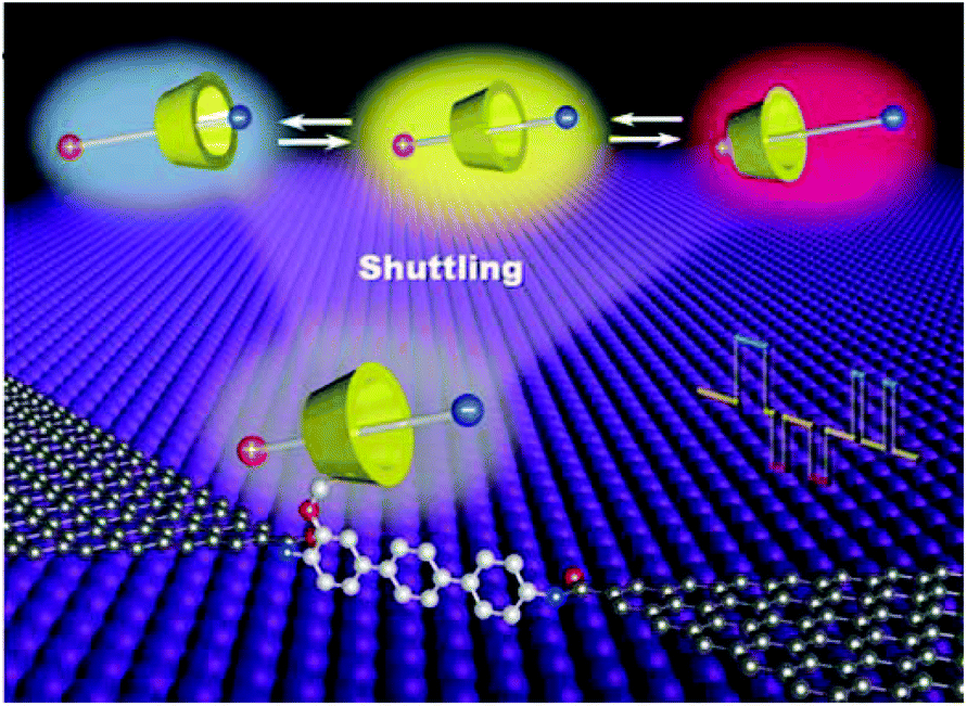 | ||
| Fig. 6 Schematic of the device structure of GMG-SMJs formed by individual molecular shuttles. Reprinted with permission from Zhou et al., Small Methods, 2019, 3, 1900464. Copyright 2019 Wiley-VCH Verlag GmbH & Co. KGaA. | ||
In order to design novel single molecule transistors, Xu et al. covalently attached individual conductive molecules including 1,4-diaminobenzene (1Ph) and 4,4′-diaminobiphenyl (2Ph) to the oxidized edges of electroburnt graphene nanogaps.36 They used reaction chemistry to bind individual conductive molecules to the oxidized edges of electroburnt graphene nanogaps. The shape and size of the graphene nanogaps provided a pathway to optimize the coupling chemistry. This led to high connection yields with ultrashort covalent single-molecule bridges (up to 40%). Therefore, extremely short molecules (as short as 0.6 nm in length) could find a way to connect into the electrical circuit chemically. The reconnection was observed after increasing the conductance across the nanogap using gate-dependent single-electron tunnelling properties. They realized that the nature of the molecule influenced the yield of reconnection.
An approach by Xin et al. presents a new avenue for engineering high-performance electronic devices based on GMG-SMJs with an ionic liquid as a gate dielectric modulating the charge transport efficiently.37 To gain more insight into the effectiveness of ionic liquid gating, three different phenyl-based molecular structures with various molecular lengths including biphenyl, triphenyl and hexaphenyl molecules were covalently coupled to graphene electrodes through amide linkages (Fig. 7). The conductance of the single-molecule junctions decreased when the length of the molecular backbone was increased. These three devices indicated gate-controlled conductance behaviour. It has been shown that the molecular length influenced the gate efficiency. When the gate voltage was changed from −1.5 V to 1.5 V, both triphenyl and hexaphenyl molecular junctions showed ambipolar charge transport characteristics. This phenomenon explained by changing of the dominant conducting orbital from HOMO to LUMO when the gate voltage was changed from negative to positive.
 | ||
| Fig. 7 (a) Switching of graphene–diarylethene junctions. (b) Molecular structures of three photochromic diarylethene. Reprinted with permission from Jia et al., Angew. Chem., Int. Ed., 2013, 52, 8666. Copyright 2013 Wiley-VCH Verlag GmbH & Co. KGaA. | ||
Sun et al.38 fabricated reliable junctions through a chemical reaction between the amino-terminated hexaphenyl aromatic molecule 4,4′-diaminohexaphenyl (DAHP) and the carboxyl groups at the edges of single-layer graphene nanoelectrodes. Hexaphenyl molecules are covalently linked to the graphene electrodes through amide linkages. They recorded I–V curves of graphene–hexaphenyl–graphene (GHG) junctions at various points after fabrication. The I–V curves before and after DAHP molecule connection were compared. When one or few molecules have been interlinked the nano-gaps, a distinct current increase was observed. In order to determine of stability of single-molecule devices, they recorded I–V curves of the same graphene–hexaphenyl–graphene (GHG) junctions at various points after fabrication. The authors did not observe any remarkable changes in the I–V curves of the GHG junctions measured immediately after fabrication, and two and four weeks after fabrication. It has been shown that more than 52% of the devices could remain stable for up to four weeks at room temperature.
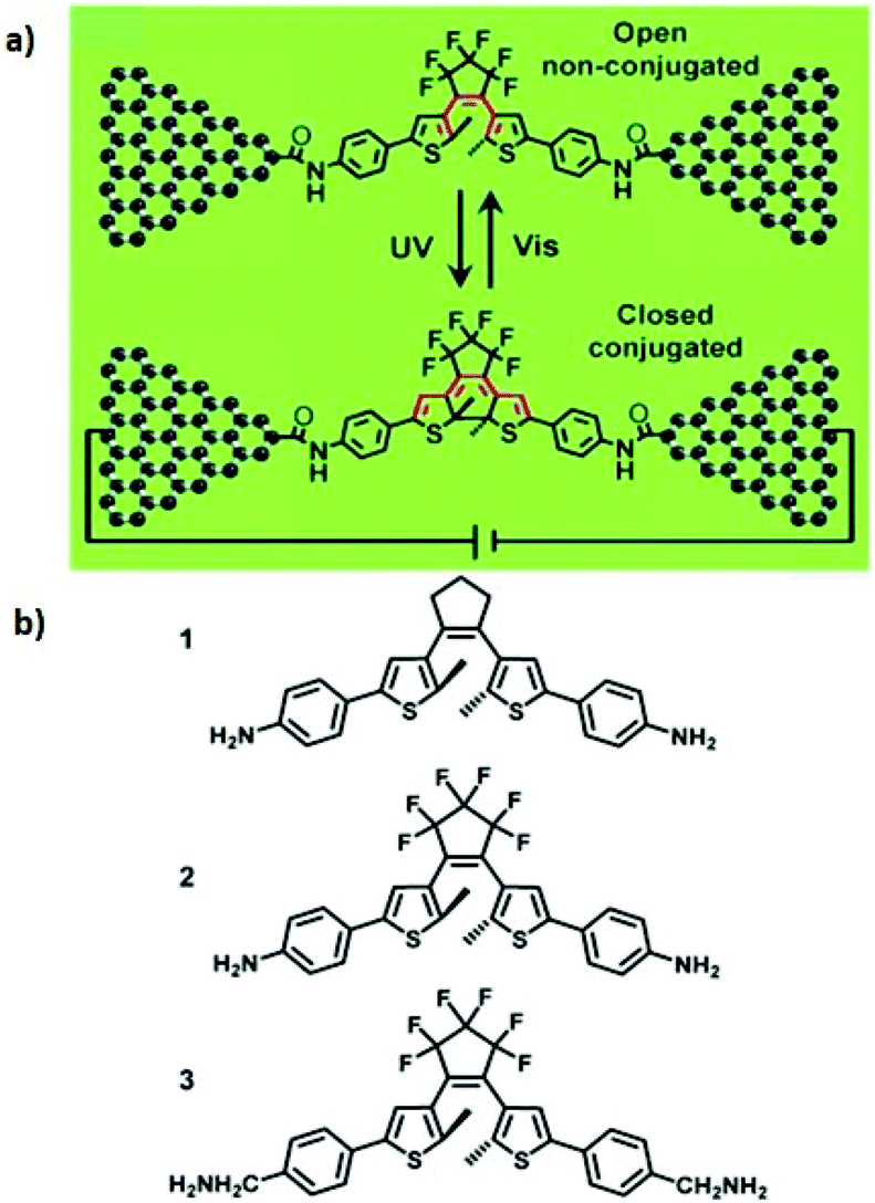
Several papers have reported to date on the design and fabrication of molecular photoswitches incorporated into graphene devices. For example, Jia et al. observed reproducible conductance switching activated by external light on a new platform of graphene–molecule junctions (Fig. 7a).39 The authors used three photochromic diarylethene derivatives with different substituents that could transition reversibly between two distinct isomers with open/closed conformations (Fig. 7b). In order to better understand the molecular energy levels at the molecule–electrode contact, they modified the interface between the graphene electrodes and the functional photoswitch by introducing methylene spacer groups. Introducing the methylene groups disturbed the π-electron delocalization between the terminal amine group and the functional centre on each side of the molecules, which led to a drop in the strong electronic coupling between the diarylethene molecules and the electrodes. The energy levels of the diarylethene derivative substituted with methylene groups were lower than those of the other two derivatives. This finding indicates that in single-molecule junctions, the on/off conductance ratios depend on the side groups outside the switching core.
In addition, Jia et al. reported the formation of stable molecular junctions by incorporating three methylene (CH2) groups covalently bound to graphene electrodes on either side of the molecular backbone (Fig. 8).40 Theoretical analysis revealed that introduction of methylene groups as molecular bridge, resulted in reduced electrode–molecule coupling which avoided the quenching of the excited molecular state by electrodes. This changed the transport regime from the Landauer regime without the CH2 groups to the Coulomb blockade regime. Furthermore, they demonstrated that the molecular junctions could perform reversible conductance photo switching in a robust way. However, the stochastic switching of the closed junction was only observed between two conductive states for the closed form between 160 to 240 K.
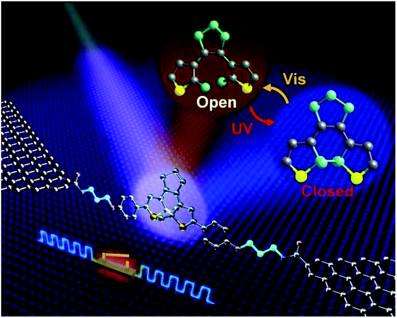 | ||
| Fig. 8 Schematic of a graphene-diarylethene-graphene junction that highlights the expansion of the molecular bridge by methylene groups. Reprinted with permission from Jia et al., Science, 2016, 352, 1443. Copy right 2016 AAAS. | ||
A different type of photoswitch based on a GMG-SMJ was introduced by Meng et al. using an azobenzene derivative, a common photochromic material with two states (cis/trans).41 Individual 2′-p-tolyldiazenyl-1,1′:4,4′-terphenyl-4,4′′-dicarboxylic acid (TTDA) molecules, were covalently attached to graphene electrodes through amide bond formation. Both the cis and trans forms of the azobenzene unit affected the electronic structure of the whole molecule. Isomerization between the states could be induced under irradiation of different wavelengths of light (UV/visible) causing different resistance display by different isomers. Both theoretical and experimental analysis confirmed that an electric field could modulate not only the energy difference between the trans and cis forms, but also the energy barrier of conformational changes.
Wu et al. theoretically determined the switching properties in a class of porphyrin molecules with pendant dipoles.42 Device fabrication involved covalent coupling of porphyrin to graphene electrodes. The porphyrin moiety was gated by a third electrode. This study revealed that by altering the number of C–C triple bonds (used as spacer units between porphyrin and graphene) from one to four, the room temperature on/off conductance ratio changed from 100 to 200. When the temperature was reduced to 100 K, this switching ratio enhanced approximately to 2200. These findings indicate that porphyrin molecular junctions can be tuned systematically by adjusting the number of spacer units.
Xin et al. investigated the stereoelectronic effect of biphenyl molecules on its electrical conductivity using robust single-molecule junctions. For this, they covalently coupled a specifically designed hexaphenyl aromatic molecule via amide bonds to graphene electrodes.43 Both theoretical and temperature-dependent experimental analysis revealed that both π–π overlap differences between the phenyl rings and two dihedral angles between the phenyl rings might result in strongly conjugated (high conductance) and weakly conjugated (low conductance) states (Fig. 9). They realized that the occurrence of stochastic switching was highly dependent on the variation in temperature. I–V analysis indicated that stochastic switching occurred between two conductance states when the temperature was increased to 120 K. It should be noted that stochastic switching at positive biases is stronger than that at negative biases. They concluded that is the asymmetric switching could be explained by the asymmetry in the two sides of graphene contacts or other unknown reasons.
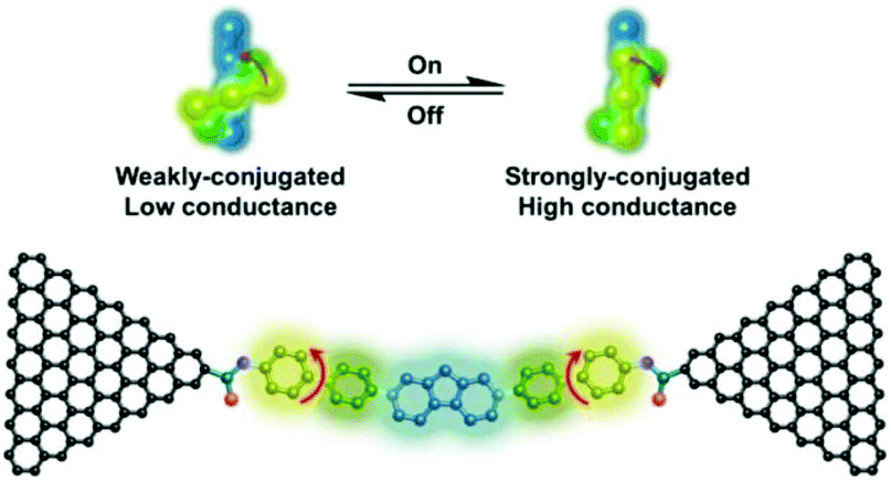 | ||
| Fig. 9 Schematic of conformational transition of terphenyl units between strongly conjugated and weakly-conjugated states and corresponding hexaphenyl aromatic chain single-molecule junctions. Reprinted with permission from Xin et al., Nano Lett., 2017, 17, 856. Copyright 2017 American Chemical Society. | ||
Graphene nanoribbons (GNRs) have also been used as electrodes for fabricating molecular devices. Unique electronic structures and transport characteristics in GNRs make them potential candidates for investigating different physical properties, such as rectification behavior negative differential resistance (NDR), switching and spin filter effect.
To investigate the conductance behavior and rectifying performance of a series of molecular diodes, Song et al. used chemical doping in an armchair edged GNR. They constructed a series of molecular diodes based on an azulene-like dipole molecule capped with chains of carbon atoms between two types of symmetrically arranged electrodes, (i) undoped zGNRs and (ii) doped armchair graphene nanoribbons (aGNRs).44 Dopants included the elements in groups III and V, boron, aluminum, nitrogen, and phosphorus located in the center positions. In addition, two carbon atoms per two carbon unit cells in an aGNRs electrode were replaced by two B or N atoms. After applying doping to the aGNR electrodes, they observed considerable rectifying behaviors with rectification ratios up to the order of 105. Compared to phosphorus dopants, the rectifying performance of aGNR electrode doped with boron and aluminum was enhanced.
Li et al. investigated the spin-dependent electron transport through a junction comprised of a single pyridine-linked (PDL) molecule with a π–σ–π building block coupled between two zigzag-edged graphene nanoribbon (zGNR) electrodes.45 For this study, they considered three different molecules including 4,4-bipyridine, 4,4′-vinylenedipyridine, and 4,4′-ethylenedipyridine. DFT calculations combined with the nonequilibrium Green's function (NEGF) formalism studies indicated that the performance of different magnetic configurations in the zGNR electrodes affected the spin-charge transport modulation. They observed the spin-filtering within the parallel (P) spin configuration and dual spin-filtering effect with antiparallel (AP) spin configuration. It is worth noting that for the junctions including a 4,4′-bipyridine molecule, the rectification ratio (RR) and the NDR effect with peak to valley ratio (PVR) could reach up to 104 and 328, respectively.
Wang et al. investigated the influence of intramolecular proton transfer on the current of single-molecule devices based on keto and enol tautomers.46 They used 6,11-dioxo-5,6,11,12 tetrahydrobenzo[b]phenazine- 1,4,7,10-tetracarbonitrile (DO-THBbPA-TCN) molecule attached covalently between two zigzag graphene nanoribbon (zGNR) electrodes (Fig. 10).47 The interconversion between the keto and enol forms occurred through intermolecular proton transfer. They found that compared to keto molecular devices, the switching effect was enhanced for the enol molecular device with an on/off ratio of up to 3.4 × 10².
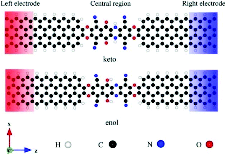 | ||
| Fig. 10 Schematic of investigated molecular junctions, where the keto and enol molecules are covalently fused into the zGNR electrodes. The left and right electrodes are denoted by the red and blue rectangles, respectively. Reprinted with permission from Wang et al., Nano Lett., 2018, 31, 17650. Copyright 2018 American Chemical Society. | ||
To understand bidirectional conductance switching, Han et al. theoretically studied the molecule–electrode interface of reversible molecular photoswitches based on diarylethene molecules.48 The molecular junctions were designed and built based on the ring-closed and ring-open forms of diarylethene molecules that were sandwiched between two monolayer graphene nanoribbons (GNRs) and two Au (111) electrodes. The photoswitching circle of the open and closed isomers was activated in both directions using irradiation with visible light. They found that the electrical conductivity and switching behavior depends on the electronic structure of molecule in both the GNRs and Au electrode. Theoretical predications indicated that the on/off current ratio of the devices could be as large as 103.
To perform two-terminal transport measurements, Li et al. designed and fabricated atomically precise single-molecule devices based on covalent bonding of a magnetic porphyrin with GNR electrodes (Fig. 11).49 They used scanning tunneling microscopy to contact the end of a linear GNR–porphyrin–GNR hybrid system via on-surface synthesis (OSS). Transport investigation revealed the spin-excitation spectral fingerprint was dependent on the connecting patterns between GNR and single molecule (SM).
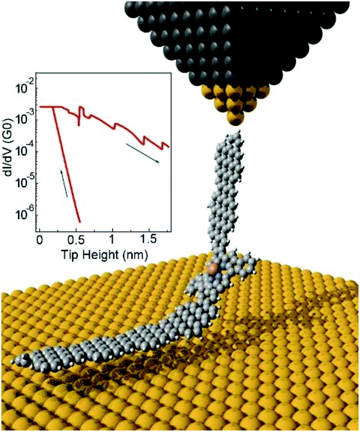 | ||
| Fig. 11 Illustration of the target experimental geometry. The inset shows a typical conductance–distance plot simultaneously recorded during tip approach and retraction. Reprinted with permission from Li et al., Nano Lett., 2019, 19, 3288. Copyright 2019 American Chemical Society. | ||
Carbon nanotubes
Carbon nanotubes (CNTs) have been used both as electric contacts at junctions and for controlling the geometry at the molecule–electrode interface.50,51 In several papers, the use of CNTs as electrodes in single molecule electronics has been reported. For example, Zhu et al.52 introduced a strategy for the fabrication of solution-processable molecular transport junctions (MTJs) covalently coupled to metallic CNT electrodes using molecular construction. DFT calculation indicated that linear junctions with two molecules embedded between two CNTs were energetically less favorable than junctions with one bridging molecule. A second molecule in the junction induced a significant strain, which increased the formation energy by ∼68 kJ mol−1 (Fig. 12). This method of fabricating MTJs could enable in future the design of different solution-processable nanoelectronics devices.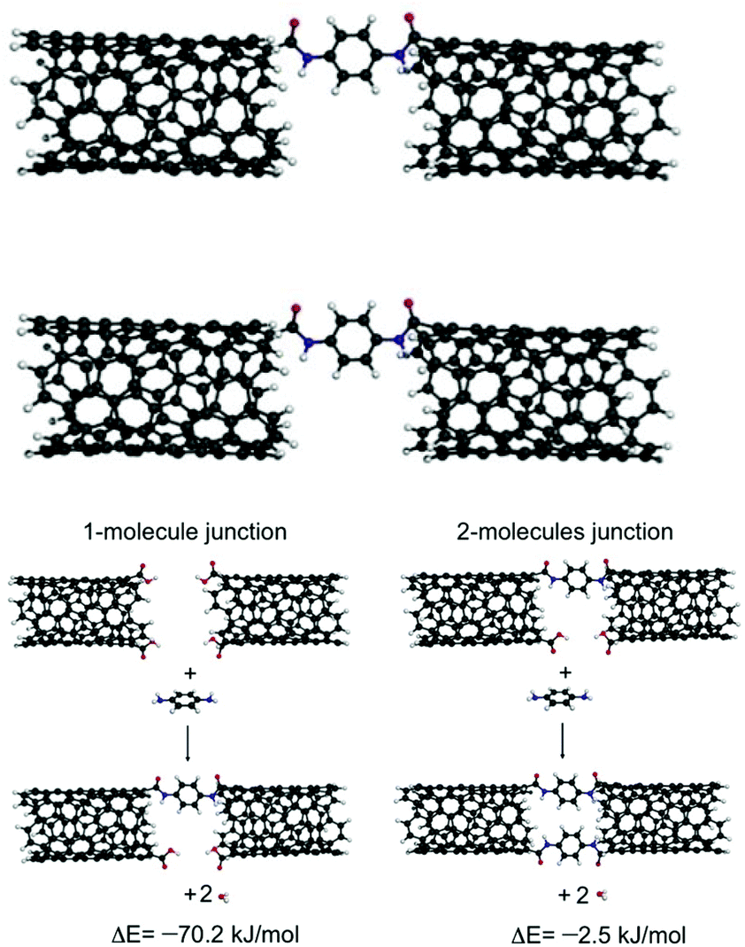 | ||
| Fig. 12 Schematic of a PPD (p-phenylenediamine)-linked molecular junction and reactions of formation for linear junctions with one and two bringing molecules. Reprinted with permission from Zhu et al., J. Am. Chem. Soc., 2016, 9, 2905. Copyright 2016 American Chemical Society. | ||
Zoppi et al. conducted a theoretical study to investigate charge transport phenomena in molecular junctions with corannulene (C20H10) covalently coupled between two CNTs.53 They investigated the influence of various design factors, such as spacer linking composition, the constitution of the active molecule element, the sensor capabilities of the active element, and the response of the nanojunction to an external electric field, on the electron transport through the CNT–[spacer]–f-C20H10–[spacer]–CNT junctions. Similarly, Sandonas et al.54 developed a comprehensive computational study indicating that heterogeneous molecular junctions, including molecular wires embedded between two different CNTs, could play the role of a selective phonon filter. They designed nanojunctions containing two colinear (6,6)-nanotubes (NTs) joined by a central molecular structure as a selective molecular-scale phonon filter.
Significant studies have been investigated in connection with biomolecular interactions at the single-molecule level for different biotechnology applications.55 Vernick et al. fabricated point-functionalized carbon nanotube transistor to measure the kinetics and thermodynamics of DNA (Deoxyribonucleic acid) hybridization for finding potential applications in genomic identification.56 They covalently attached an amine-modified oligonucleotide probe to a single defect site, generated on the single-walled carbon nanotubes (SWCNT) sidewall. In this study, the CNT played the role as the channel of a field-effect transistor.
In order to measure the conductivity a single DNA duplex coupled with a carbon electrode, Guo et al. integrated two amine-modified DNAs to the SWCNTs electrodes through covalent bonds.57 They observed modification of DNA sequences with amines on either the 5′ terminus or both the 3′ and 5′ termini led to a resistance on the order of 1 MΩ. Likewise, Sorgenfrei et al. covalently attached the probe DNA, terminated with an amine group and a three-carbon linker at the 5′ end to the point defect in a carbon nanotube.58 It has been shown that this novel single molecule label-free bioanalytical system could probe molecular kinetics at microsecond timescales.
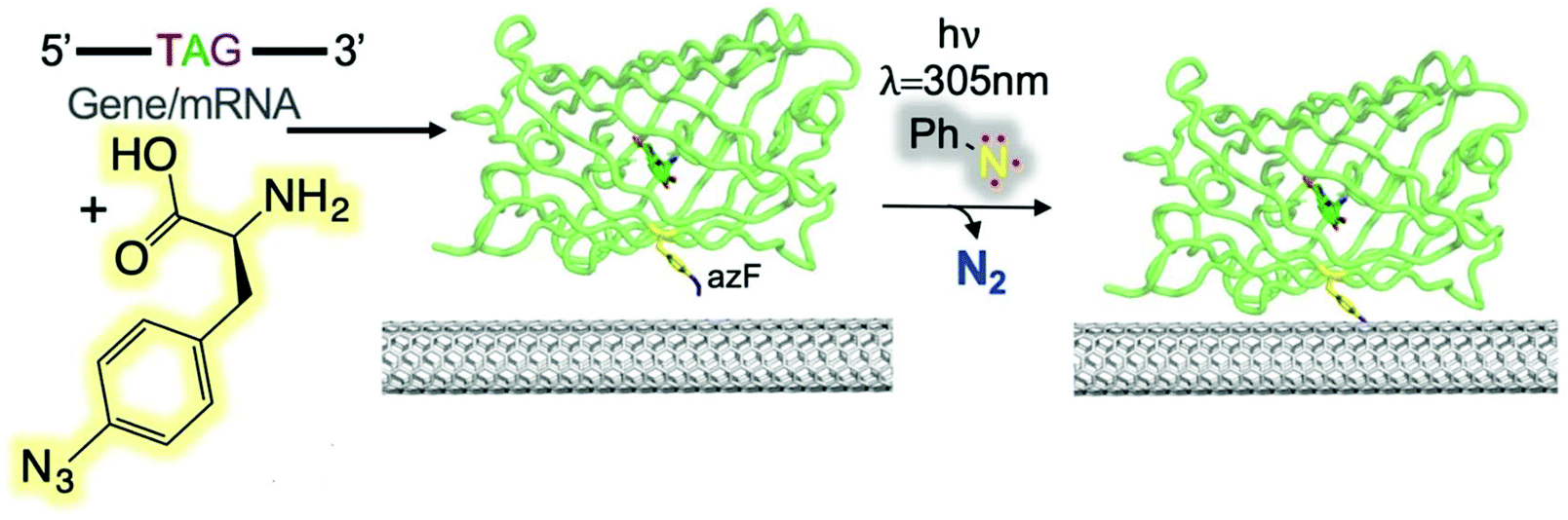
Freeley et al. conducted a study to investigate the covalent coupling of single proteins to the terminal ends of individual SWCNTs using an in-solution methodology.59 They designed two green fluorescent protein (sfGFP) variants to introduce an azide CNT-anchoring handle. The two GFP mutants (short axis, GFPSA and long axis, GFPLA) were constructed to form ssDNA/SWCNT-GFP hybrids with specific protein orientations. Florescence investigation revealed the evidence of site-specific coupling between the SWCNTs and the proteins for only the SWCNT-GFPSA nanohybrids. Recently, Thomas et al. reported the covalent coupling of four different fluorescent proteins to CNT side walls through phenyl azide photochemistry (Fig. 13).60 Depending on the position of the protein on the CNT side wall, GFP function switched from GFPLA and GFPSA, which resulted in a change of the fluorescence wavelength.
 | ||
| Fig. 13 Direct protein attachment to CNTs via phenyl azide photochemistry. Scheme of photochemical insertion of a protein via genetically encoded phenyl azide chemistry. Reprinted with permission from Thomas et al., Bioconjugate Chem., 2019, 3, 584. | ||
Choi et al. developed an approach to monitor single-molecule lysozyme dynamics by attaching the molecule of interest to a field-effect transistor (FET) device using a noncovalent immobilization based on pyrene linkers.61 The binding of pyrenes to SWNTs through π–π stacking might pave the pathway for dilute anchor points for further derivatization of the surface. In this study, a thiol from a single cysteine variant of T4 lysozyme (S90C) was covalently coupled to a pyrene maleimide anchor site. Recently, Nakanishi et al. encapsulated single-molecule magnets (SMMs) based on the endohedral metallofullerene DySc2N@C80 into the internal 1D nanospace of single-walled carbon nanotubes (Fig. 14).62 This succeeded because of the strong π–π interactions of SWCNTs with encapsulated fullerenes which are commonly called “peapods” and have shown to be able to modulate electrical properties in SWCNTs.
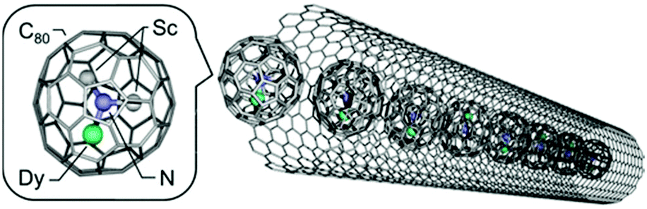 | ||
| Fig. 14 Image of DySc2N@C80 (left) and DySc2N@C80 encapsulated in an SWCNT (right). Reprinted with permission from Nikanishi et al., J. Am. Chem. Soc., 2018, 35, 10955. Copyright 2018 American Chemical Society. | ||
Conclusions and outlook
As discussed above, different methods have been investigated for fabrication of reliable single molecule electronics. However, there are still several challenges when it comes to rationale design and engineering of stable carbon-based molecular junctions.One of the key issues is device stability which arises due to the oxidation of metallic electrodes in air and electromigration. This results in poor reproducibility of the formation of metal–molecule–metal junctions. The strong sp2 C–C covalent bonds in graphene can increase the possibility of stable nanogaps formation. It should be mentioned here that considerable device stability of carbon-based molecular junctions formed via covalent amide linkage has been observed up to 4 weeks at ambient temperature.
Another formidable challenge is controlling the molecule–electrode interface. Compared to metallic electrode, the use of (sp2-) carbon-based materials allows a wide range of possibility to anchor different molecules. The π-stacking of large π-conjugated anchor groups can mitigate the differences in the level broadening (Γ) by averaging the interaction over a larger interfacial area and also leads to improvements in device yield.23 The modification in the molecule–electrode coupling changes the level broadening (Γ) and subsequently the conductance through the junctions. However, there are still some questions regarding how different parameters such Γ is modulated under the influence of the edge chemistry of the graphene. Manipulating the structure of molecular bridges by adding more side groups and spacers might be another potential solution. The modification of the interface between the graphene and electrodes by incorporating spacer groups, the on/off conductance ratios for a series of photoswitches were shown to be changed significantly. This finding can serve as a promising future for reliable fabrication of photoswitch based on a GMG-SMJ.
To achieve reproducible atomic size fabrication of nanogaps, single-molecule electronics can be a potential alternative to Si-based microelectronics in the future. Recently, works on dynamic process at the single molecule level including host–guest interactions, hydrogen bond interactions and studying of physical, chemical, and biological processes using the GMG-SMJ platform have been reported. Therefore, this field of research is growing to introduce brand new functions which can lead to new applications. Recently there are several reports regarding the interaction of 2D materials with biomolecules such as DNA.63,64 DNA sequencing could be assessed through the formation of nanogap by the lateral heterostructure of graphene and hexagonal boron nitride (h-BN) classified as 2D materials.65 The passivation of the edge of graphene electrode with h-BN could be a viable solution for addressing the practical challenges when it comes to high reactivity and controlling the engineering of graphene edge structure. In this context, a recent development that may create new avenues for single molecule electronics is transition metal dichalcogenide metamaterials that can be manipulated with atomic precision to lead point contacts.66
Graphene nanostructure have been widely used as single-molecule biosensors with focus on DNA sequencing applications. One notable issue which should be taken into account is noise characteristics of graphene structures with sizes on the order of a few nanometres. Recently, Fried et al., investigated the noise characteristics of a graphene quantum dot at room temperature in liquid environments.67 Unlike reported studies,68 they observed that the noise was significantly independent of the liquid environment and the substrate. In this study, the noise was attributed to charge trapping and detrapping at the disordered graphene edges. In order to improve the potential of graphene nanodevices in applications such as single molecule biosensing, the high noise level and presence of two-level fluctuations should be carefully addressed. This issue serve as another challenge in this field as some studies on the noise characteristics of graphene structures have been reported at cryogenic temperatures and under high vacuum.68,69
Conflicts of interest
There are no conflicts to declare.Acknowledgements
The authors would like to acknowledge the Chalmers Foundation for financial support.Notes and references
- M. Y. Li, S. K. Su, H. S. P. Wong and L. J. Li, Nature, 2019, 567, 169–170 CrossRef CAS.
- I. Franco, C. B. George, G. C. Solomon, G. C. Schatz and M. A. Ratner, J. Am. Chem. Soc., 2011, 133, 2242–2249 CrossRef CAS.
- Z. Donhauser, B. Mantooth, K. Kelly, L. Bumm, J. Monnell, J. J. Stapleton, D. Price, A. Rawlett, D. Allara and J. Tour, Science, 2001, 292, 2303–2307 CrossRef CAS.
- J. L. Zhang, J. Q. Zhong, J. D. Lin, W. P. Hu, K. Wu, G. Q. Xu, A. T. Wee and W. Chen, Chem. Soc. Rev., 2015, 44, 2998–3022 RSC.
- B. Capozzi, J. Xia, O. Adak, E. J. Dell, Z.-F. Liu, J. C. Taylor, J. B. Neaton, L. M. Campos and L. Venkataraman, Nat. Nanotechnol., 2015, 10, 522–527 CrossRef CAS.
- I. Díez-Pérez, J. Hihath, Y. Lee, L. Yu, L. Adamska, M. A. Kozhushner, I. I. Oleynik and N. Tao, Nat. Chem., 2009, 1, 635–641 CrossRef.
- J. Park, A. N. Pasupathy, J. I. Goldsmith, C. Chang, Y. Yaish, J. R. Petta, M. Rinkoski, J. P. Sethna, H. D. Abruña and P. L. McEuen, Nature, 2002, 417, 722–725 CrossRef CAS.
- J. Hwang, M. Pototschnig, R. Lettow, G. Zumofen, A. Renn, S. Götzinger and V. Sandoghdar, Nature, 2009, 460, 76–80 CrossRef CAS.
- R. M. Metzger, Chem. Rev., 2015, 115, 5056–5115 CrossRef CAS.
- P. Song, S. Guerin, S. J. R. Tan, H. V. Annadata, X. Yu, M. Scully, Y. M. Han, M. Roemer, K. P. Loh and D. Thompson, Adv. Mater., 2018, 30, 1706322 CrossRef.
- Y. Ai, A. Kovalchuk, X. Qiu, Y. Zhang, S. Kumar, X. Wang, M. Kühnel, K. Nørgaard and R. C. Chiechi, Nano Lett., 2018, 18, 7552–7559 CrossRef CAS.
- L. Cao, L. Yuan, M. Yang, N. Nerngchamnong, D. Thompson, X. Yu, D.-C. Qi and C. A. Nijhuis, Nanoscale Adv., 2019, 1, 1991–2002 RSC.
- L. Sun, Y. A. Diaz-Fernandez, T. A. Gschneidtner, F. Westerlund, S. Lara-Avila and K. Moth-Poulsen, Chem. Soc. Rev., 2014, 43, 7378–7411 RSC.
- A. Bergvall, K. Berland, P. Hyldgaard, S. Kubatkin and T. Löfwander, Phys. Rev. B: Condens. Matter Mater. Phys., 2011, 84, 155451 CrossRef.
- Y. Xue and M. A. Ratner, Int. J. Quantum Chem., 2005, 102, 911–924 CrossRef CAS.
- J. Hihath and N. Tao, Semicond. Sci. Technol., 2014, 29, 054007 CrossRef.
- C. Jia and X. Guo, Chem. Soc. Rev., 2013, 42, 5642–5660 RSC.
- M. El Abbassi, S. Sangtarash, X. Liu, M. L. Perrin, O. Braun, C. Lambert, H. S. J. van der Zant, S. Yitzchaik, S. Decurtins and S.-X. Liu, Nat. Nanotechnol., 2019, 14, 957–961 CrossRef CAS.
- Z. Tan, D. Zhang, H.-R. Tian, Q. Wu, S. Hou, J. Pi, H. Sadeghi, Z. Tang, Y. Yang and J. Liu, Nat. Commun., 2019, 10, 1–7 CrossRef CAS.
- S. Leitherer, P. B. Coto, K. Ullmann, H. B. Weber and M. Thoss, Nanoscale, 2017, 9, 7217–7226 RSC.
- K. Ullmann, P. B. Coto, S. Leitherer, A. Molina-Ontoria, N. Martín, M. Thoss and H. B. Weber, Nano Lett., 2015, 15, 3512–3518 CrossRef CAS.
- A. V. Danilov, P. Hedegård, D. S. Golubev, T. Bjørnholm and S. E. Kubatkin, Nano Lett., 2008, 8, 2393–2398 CrossRef CAS.
- B. Limburg, J. O. Thomas, G. Holloway, H. Sadeghi, S. Sangtarash, I. C. Y. Hou, J. Cremers, A. Narita, K. Müllen and C. J. Lambert, Adv. Funct. Mater., 2018, 28, 1803629 CrossRef.
- E. Burzurí, A. García-Fuente, V. García-Suárez, K. S. Kumar, M. Ruben, J. Ferrer and H. S. van der Zant, Nanoscale, 2018, 10, 7905–7911 RSC.
- C. S. Lau, H. Sadeghi, G. Rogers, S. Sangtarash, P. Dallas, K. Porfyrakis, J. Warner, C. J. Lambert, G. A. D. Briggs and J. A. Mol, Nano Lett., 2016, 16, 170–176 CrossRef CAS.
- H. Sadeghi, S. Sangtarash and C. Lambert, Nano Lett., 2017, 17, 4611–4618 CrossRef CAS.
- C. Lambert, Chem. Soc. Rev., 2015, 44, 875–888 RSC.
- F. Prins, A. Barreiro, J. W. Ruitenberg, J. S. Seldenthuis, N. Aliaga-Alcalde, L. M. Vandersypen and H. S. van der Zant, Nano Lett., 2011, 11, 4607–4611 CrossRef CAS.
- E. Burzurí, J. O. Island, R. Díaz-Torres, A. Fursina, A. González-Campo, O. Roubeau, S. J. Teat, N. Aliaga-Alcalde, E. Ruiz and H. S. van der Zant, ACS Nano, 2016, 10, 2521–2527 CrossRef.
- J. A. Mol, C. S. Lau, W. J. Lewis, H. Sadeghi, C. Roche, A. Cnossen, J. H. Warner, C. J. Lambert, H. L. Anderson and G. A. D. Briggs, Nanoscale, 2015, 7, 13181–13185 RSC.
- C. Gu, C. Hu, Y. Wei, D. Lin, C. Jia, M. Li, D. Su, J. Guan, A. Xia and L. Xie, Nano Lett., 2018, 18, 4156–4162 CrossRef CAS.
- J. Guan, C. Jia, Y. Li, Z. Liu, J. Wang, Z. Yang, C. Gu, D. Su, K. N. Houk and D. Zhang, Sci. Adv., 2018, 4, eaar2177 CrossRef.
- C. Zhou, X. Li, Z. Gong, C. Jia, Y. Lin, C. Gu, G. He, Y. Zhong, J. Yang and X. Guo, Nat. Commun., 2018, 9, 1–9 CrossRef.
- H. Wen, W. Li, J. Chen, G. He, L. Li, M. A. Olson, A. C.-H. Sue, J. F. Stoddart and X. Guo, Sci. Adv., 2016, 2, e1601113 CrossRef.
- C. Zhou, X. Li, H. Masai, Z. Liu, Y. Lin, T. Tamaki, J. Terao, J. Yang and X. Guo, Small Methods, 2019, 3, 1900464 CrossRef CAS.
- Q. Xu, G. Scuri, C. Mathewson, P. Kim, C. Nuckolls and D. Bouilly, Nano Lett., 2017, 17, 5335–5341 CrossRef CAS.
- N. Xin, X. Li, C. Jia, Y. Gong, M. Li, S. Wang, G. Zhang, J. Yang and X. Guo, Angew. Chem., 2018, 130, 14222–14227 CrossRef.
- H. Sun, Z. Jiang, N. Xin, X. Guo, S. Hou and J. Liao, ChemPhysChem, 2018, 19, 2258–2265 CrossRef CAS.
- C. Jia, J. Wang, C. Yao, Y. Cao, Y. Zhong, Z. Liu, Z. Liu and X. Guo, Angew. Chem., Int. Ed., 2013, 52, 8666–8670 CrossRef CAS.
- C. Jia, A. Migliore, N. Xin, S. Huang, J. Wang, Q. Yang, S. Wang, H. Chen, D. Wang and B. Feng, Science, 2016, 352, 1443–1445 CrossRef CAS.
- L. Meng, N. Xin, C. Hu, J. Wang, B. Gui, J. Shi, C. Wang, C. Shen, G. Zhang and H. Guo, Nat. Commun., 2019, 10, 1–8 CrossRef CAS.
- Q. Wu, S. Hou, H. Sadeghi and C. J. Lambert, Nanoscale, 2018, 10, 6524–6530 RSC.
- N. Xin, J. Wang, C. Jia, Z. Liu, X. Zhang, C. Yu, M. Li, S. Wang, Y. Gong and H. Sun, Nano Lett., 2017, 17, 856–861 CrossRef CAS.
- Y. Song, Z. Xie, Y. Ma, Z.-L. Li and C.-K. Wang, J. Phys. Chem. C, 2014, 118, 18713–18720 CrossRef CAS.
- X. Li, L. Cao, H.-L. Li, H. Wan and G. Zhou, J. Phys. Chem. C, 2016, 120, 3010–3018 CrossRef CAS.
- Z.-Q. Wang, M.-Z. Wei, M.-M. Dong, G.-C. Hu, Z.-L. Li, C.-K. Wang and G.-P. Zhang, J. Phys. Chem. C, 2018, 122, 17650–17659 CrossRef CAS.
- D. Weckbecker, P. Coto and M. Thoss, Nano Lett., 2017, 17, 3341–3346 CrossRef CAS.
- L. Han, X. Zuo, H. Li, Y. Li, C. Fang and D. Liu, J. Phys. Chem. C, 2019, 123, 2736–2745 CrossRef CAS.
- J. Li, N. Friedrich, N. Merino, D. G. de Oteyza, D. Peña, D. Jacob and J. I. Pascual, Nano Lett., 2019, 19, 3288–3294 CrossRef CAS.
- X. Guo, J. P. Small, J. E. Klare, Y. Wang, M. S. Purewal, I. W. Tam, B. H. Hong, R. Caldwell, L. Huang and S. O'Brien, Science, 2006, 311, 356–359 CrossRef CAS.
- A. K. Feldman, M. L. Steigerwald, X. Guo and C. Nuckolls, Acc. Chem. Res., 2008, 41, 1731–1741 CrossRef CAS.
- J. Zhu, J. McMorrow, R. Crespo-Otero, G. Ao, M. Zheng, W. P. Gillin and M. Palma, J. Am. Chem. Soc., 2016, 138, 2905–2908 CrossRef CAS.
- L. Zoppi, A. Ferretti and K. K. Baldridge, J. Chem. Theory Comput., 2015, 11, 4900–4910 CrossRef CAS.
- L. Medrano Sandonas, Á. Rodríguez Méndez, R. Gutierrez, J. M. Ugalde, V. Mujica and G. Cuniberti, J. Phys. Chem. C, 2019, 123, 9680–9687 CrossRef CAS.
- S. Sorgenfrei, C.-Y. Chiu, M. Johnston, C. Nuckolls and K. L. Shepard, Nano Lett., 2011, 11, 3739–3743 CrossRef CAS.
- S. Vernick, S. M. Trocchia, S. B. Warren, E. F. Young, D. Bouilly, R. L. Gonzalez, C. Nuckolls and K. L. Shepard, Nat. Commun., 2017, 8, 1–9 CrossRef.
- X. Guo, A. A. Gorodetsky, J. Hone, J. K. Barton and C. Nuckolls, Nat. Nanotechnol., 2008, 3, 163–167 CrossRef CAS.
- S. Sorgenfrei, C.-Y. Chiu, R. L. Gonzalez Jr., Y.-J. Yu, P. Kim, C. Nuckolls and K. L. Shepard, Nat. Nanotechnol., 2011, 6, 126 CrossRef CAS.
- M. Freeley, H. L. Worthy, R. Ahmed, B. Bowen, D. Watkins, J. E. Macdonald, M. Zheng, D. D. Jones and M. Palma, J. Am. Chem. Soc., 2017, 139, 17834–17840 CrossRef CAS.
- S. K. Thomas, W. D. Jamieson, R. E. Gwyther, B. J. Bowen, A. Beachey, H. L. Worthy, J. E. Macdonald, M. Elliott, O. K. Castell and D. D. Jones, Bioconjugate Chem., 2019, 31, 584–594 CrossRef.
- Y. Choi, I. S. Moody, P. C. Sims, S. R. Hunt, B. L. Corso, I. Perez, G. A. Weiss and P. G. Collins, Science, 2012, 335, 319–324 CrossRef CAS.
- R. Nakanishi, J. Satoh, K. Katoh, H. Zhang, B. K. Breedlove, M. Nishijima, Y. Nakanishi, H. Omachi, H. Shinohara and M. Yamashita, J. Am. Chem. Soc., 2018, 140, 10955–10959 CrossRef CAS.
- Q. Li, H. Liu, Y. Tian, J. Guo, G. Chen and J. Y. Lee, J. Phys. Chem. C, 2020, 124, 10823–10831 CrossRef CAS.
- R. L. Kumawat and B. Pathak, J. Phys. Chem. C, 2019, 123, 22377–22383 CrossRef CAS.
- V. Shukla, N. K. Jena, A. Grigoriev and R. Ahuja, ACS Appl. Mater. Interfaces, 2017, 9, 39945–39952 CrossRef CAS.
- B. Munkhbat, A. B. Yankovich, D. G. Baranov, R. Verre, E. Olsson and T. O. Shegai, Nat. Commun., 2020, 11, 1–8 Search PubMed.
- J. P. Fried, X. Bian, J. L. Swett, I. I. Kravchenko, G. A. D. Briggs and J. A. Mol, Nanoscale, 2020, 12, 871–876 RSC.
- X.-X. Song, H.-O. Li, J. You, T.-Y. Han, G. Cao, T. Tu, M. Xiao, G.-C. Guo, H.-W. Jiang and G.-P. Guo, Sci. Rep., 2015, 5, 8142 CrossRef CAS.
- P. Puczkarski, Q. Wu, H. Sadeghi, S. Hou, A. Karimi, Y. Sheng, J. H. Warner, C. J. Lambert, G. A. D. Briggs and J. A. Mol, ACS Nano, 2018, 12, 9451–9460 CrossRef CAS.
| This journal is © The Royal Society of Chemistry 2021 |