
Exploring the behaviors of electrode-driven Si quantum dot systems: from charge control to qubit operations†
Ji-Hoon
Kang‡
 ,
Junghee
Ryu
and
Hoon
Ryu‡
*
,
Junghee
Ryu
and
Hoon
Ryu‡
*
Division of National Supercomputing, Korea Institute of Science and Technology Information, Daejeon 34141, Republic of Korea. E-mail: elec1020@kisti.re.kr; Tel: +82 42 869 0610
First published on 27th November 2020
Abstract
Charge stabilities and spin-based quantum bit (qubit) operations in Si double quantum dot (DQD) systems, whose confinement potentials are controlled with multiple gate electrodes, are theoretically studied with a multi-scale modeling approach that combines electronic structure simulations and the Thomas–Fermi method. Taking Si/SiGe heterostructures as the target of modeling, this work presents an in-depth discussion on the designs of electron reservoirs, electrostatic controls of quantum dot (QD) shapes and their corresponding charge confinements, and spin qubit manipulations. The effects of unintentional inaccuracies in DC control biases and geometric symmetries on the Rabi cycle of spin qubits are investigated to examine the robustness of logic operations. Solid connections to the latest experimental results are also established to validate the simulation method. As a rare modeling study that explores the full-stack functionality of Si DQD structures as quantum logic gate devices, this work delivers the knowledge of engineering details that are not uncovered by the latest experimental work and can serve as a basic but practical guideline for potential device designs.
1 Introduction
Semiconductors have been regarded as attractive materials for the designing of universal quantum logic gates mainly due to their advantage of easy integration with classical control hardware using an industry-standard fabrication process. In particular, semiconductor quantum dot (QD) structures have been extensively studied as an emerging platform for building quantum logic gate blocks,1–10 where quantum bits (qubits) are encoded as either charges or spins of the confined states and can be manipulated by controlling the biases applied on the external electrodes. Gallium–arsenide (GaAs) has been widely adopted to create physical layers of carrier confinement due to its high electron mobility.1,2 However, the broken inversion-symmetry originating from the crystal anisotropies of GaAs layers of a few nanometer (nm) scale11,12 serves as a major factor that causes electric/magnetic field noises and band gap fluctuations, making stable qubit operations difficult.13 Silicon (Si) has also attracted considerable attention for qubit designs since it can be easily procured and in principle consists of an inversion-symmetric crystal. It has been well known that the weak spin–orbit interaction of Si drives a long spin-lifetime,14 and that the coherence of electron spins can be retained up to 30 seconds in isotopically enriched 28Si.15 With the rapid progress in today's lithographic technology, it is now possible to procure 300 mm 28Si wafers whose purity reaches 99.99%,16,17 and successful synthesis of 99.999% enriched 28Si crystals has been also reported.18Though qubits can be encoded using charges that are confined in Si nanostructures,5,19,20 due to the above-mentioned reasons, spin-based qubit encoding has been actively studied during the last decade,3,4,6–10 and electron spin qubits in Si QD structures are known to be able to retain their quantum states ∼103 times longer than other competing technologies such as superconducting qubits.21,22 Based upon the seminal work of Loss and DiVincenzo who conceptually proposed the designs of logic gate devices with electron spins in double quantum dot (DQD) systems,23 experimentalists have devoted huge efforts to investigating Si-based DQD systems. A successful coherent control of electron spins in Si DQDs was demonstrated by Maune et al.3 Veldhorst et al. then reported the individual addressability of multiple spin qubits6 and realized controlled-NOT (CNOT) gates by combining controlled-phase operations and 1-qubit operations.7 Zajac et al. reported ∼3× faster CNOT gates involving a single control step,8 and, most recently, Watson et al. demonstrated the successful implementation of a programmable 2-qubit quantum processor using the Si DQD platform, which has the capability to solve the Deutsch–Jozsa and Grover algorithms.9
Despite all the above-mentioned experimental efforts, there are still issues that should be examined for a better understanding of Si DQD quantum gates from the perspective of device design. The two issues that need urgent clarification, in particular, can be (1) the robustness of gate designs against any unintentional inaccuracy in design factors (unintentional inaccuracy would essentially occur in the real world scenario) and (2) the margin of control signals in which the stability of quantum logic operations can be guaranteed. An elaborate study of these issues needs to be pursued with computer-aided simulations since the experimental investigations of all the design variations would involve huge time and expense, and is non-trivial since it not only presents a formalized design guideline but can also invoke potential efforts to evolve the existing device designs towards advanced regimes. Accordingly, herein we propose a multi-scale scheme of device simulations that combines a semi-classical Thomas–Fermi model24 and electronic structure calculations based on a parabolic effective mass theory.25 Taking a recently reported Si DQD structure as a modeling target,8 we discuss the designs of a low-temperature 2D electron gas (2DEG) that is essential to secure DQD-embedded ohmic contacts. The full charge stability diagram is then modeled to explore the controllability of the DC biases applied on the three key gate electrodes, and the range of the control biases applicable for qubit initialization is investigated. By taking the control biases and the dimensions of the gate electrodes as factors subject to unintentional inaccuracy, the robustness of logic operations is also discussed by simulating 2-qubit time responses under a weak correlation. As a full-stack modeling study digging out engineering details that have not been clarified in previous studies, this work will contribute to extending the knowledge on the designs of Si quantum logic gates based on electrode-driven DQDs structures.
2 Methods
The DQD structure to be modeled is based on a heterostructure consisting of Si and SiGe layers similar to a previously reported structure.8Fig. 1(a) and (b) show a conceptual illustration of the reported DQD structure and a simulation domain used in this work, respectively. The domain is assumed to be 2D, as the size of the physically realized structure is quite long (∼0.1 μm) along the [001] direction (Z). A vertical quantum confinement (along the [010] direction (Y)) is naturally formed in the middle Si layer by the conduction band offset between the Si and Si0.7Ge0.3 layers. Inside the middle Si layer, a lateral confinement (along the [100] direction (X)) can be created by applying appropriate biases on the top gate electrodes so the target structure can have up to 2 QDs. In the simulations, these gate electrodes are taken into account by imposing a Dirichlet boundary condition with finite biases and Schottky barriers (ϕB) on a 2D Poisson equation. The ϕB values of all the top electrodes are calculated using the work-functions reported for metal electrodes consisting of Ti/Au layers.26 At both ends of the middle Si layer along the [100] direction, which serve as source/drain electron reservoirs, a Dirichlet boundary condition with ϕB = 0 is imposed by assuming that the leads are ohmic, and 2DEGs are formed well. A static magnetic field (BZ) is assumed to be applied along the [001] direction with a gradient along the [100] direction (∂BZ/∂X) to make the Zeeman splittings of the two QD ground states distinguishable, where the BZ distribution is taken from the stray field profile simulated for a horseshoe-shaped cobalt micro-magnet27, which is also employed in the experiment.8 An AC magnetic field (BY), whose magnitude and frequency are control variables, is applied along the [010] direction to drive logic operations. Two-qubit time responses are simulated by solving a time-dependent Schrödinger equation coupled to the Heisenberg Hamiltonian of two neighboring spins.28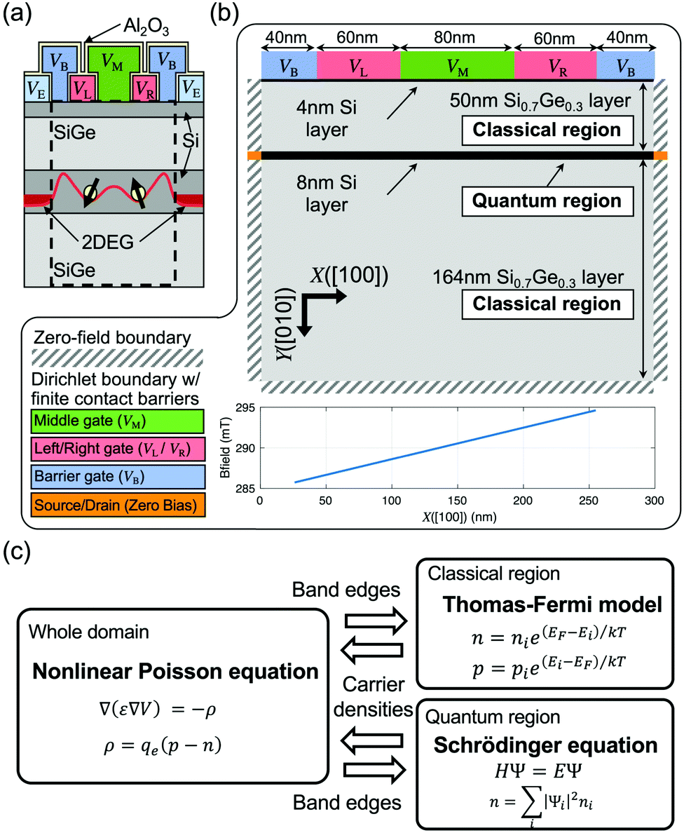 | ||
| Fig. 1 Simulation domain and modeling approach. (a) A conceptual 2D description of the Si double quantum dot (DQD) structure reported in ref. 8. QDs are created in the middle Si layer by controlling the left (VL), middle (VM), and right (VR) gate bias, where the barrier gate bias (VB) is used to separate the QDs and 2D electron gases (2DEG). (b) A 2D simulation domain. The 2DEG regions are considered with a Dirichlet boundary condition coupled to the zero Schottky barrier height. A spatial distribution of the magnetic field along the [001] (Z) direction is taken from the stray field profile simulated for a cobalt micro-magnet in ref. 26. (c) A numerical flow of simulations. Given a potential profile, a charge profile is obtained in two ways: electronic structure calculations with a parabolic effective mass model (applied to the middle Si layer labeled as the quantum region in (a)) and Thomas–Fermi calculations (the other region labeled as the classical region in (a)). With a charge profile, a nonlinear Poisson equation is solved to achieve a new potential profile. These processes is repeated until the potential profile converges. | ||
For the self-consistent determination of the electrostatic profiles in the target DQD structure, we implemented a hybrid modeling approach using the numerical flow shown in Fig. 1(c). Given an initial potential profile, a spatial charge distribution is calculated using either a simple semi-classical Thomas–Fermi (TF) method24 or electronic structure simulations coupled with a single-band effective mass approach (EMA).25 The methodological choice for the charge calculations depends on the region of interest in the simulation domain. For a region that can be assumed to have no charges at very low temperatures (labeled as the Classical Region in Fig. 1(b)), the TF method is employed since there are no critical needs for quantum mechanical solutions that require a huge computing expense. In the middle Si layer and its surrounding region where the confined electrons are expected to reside (labeled as the Quantum Region in Fig. 1(b)), however, an EMA-based Schröedinger equation is solved for the precise prediction of quantized energy levels and spatial distributions of electron wavefunctions (note that the ESI† presents a more detailed explanation about how the EMA is used to model the electron spin-states in this work). Once the charge profile is determined, we solve a nonlinear 2D Poisson equation (with boundary conditions addressed in the previous paragraph)29 to obtain a new potential profile that will be again be used to obtain a new charge distribution unless the potential profile satisfies a user-defined convergence criterion (a mean square error less than 10−10 eV in our case). For all the modeling works, we assume a temperature (T) of 1.5 K.
3 Results and discussion
The first focal point of discussion in this section is the formation of 2DEG, which has huge importance in the DQD-based designs of quantum logic gates, as it acts as an electron reservoir that enables the injection of carriers into the DQD channel. To examine the design conditions of 2DEGs in Si/SiGe layers whose thickness and alloy composition are identical to the ones shown in Fig. 1(b), we performed simulations with a 2D domain that had a single top electrode as shown in Fig. 2(a). A Dirichlet boundary condition (with a bias of VE) was imposed on a Poisson equation to describe the top surface. A zero-field boundary was used for the other three surfaces, as the physical structure would be very long along +X, −X, and +Y directions.8 The spatial distribution of the conduction band minimum (EC) simulated at VE = 430 mV is shown in Fig. 2(b), where the Fermi-energy (EF) was set to zero. A potential barrier of ∼0.2 eV, observed at the interface of Si/SiGe layers due to the conduction band offset, confined electrons along the [010] direction. Along the [100] direction, however, electrons were not confined. Therefore, once electrons existed in the middle Si layer, they could move freely along the [100] direction forming a 2DEG, as the simulation domain was assumed to be infinitely long along the [001] direction. Electrons can fill the middle Si layer by increasing VE, as shown in Fig. 2(c), where we plotted the 1D-cuts of VE-dependent EC profiles along the [010] direction. Increasing VE lowers EC, and, in our results, the ground state in a quantum well formed by the middle Si layer becomes lower in energy than EF when VE ≥ 430mV, being occupied with an electron. Fig. 2(d) and (e) show the electron density profiles (ρ) at VE = 430 mV and their 1D-cuts along the [010] direction, respectively, and both profiles have a maximum value of ∼4 × 1022 cm−3 at the center of the middle Si layer and are uniform along the [100] direction. The 1D-cuts of the EC profiles along the [010] direction at VE = 427–430 mV are shown in Fig. 2(f), indicating that increasing VE does not necessarily lower EC due to the screening effect once 2DEG is created.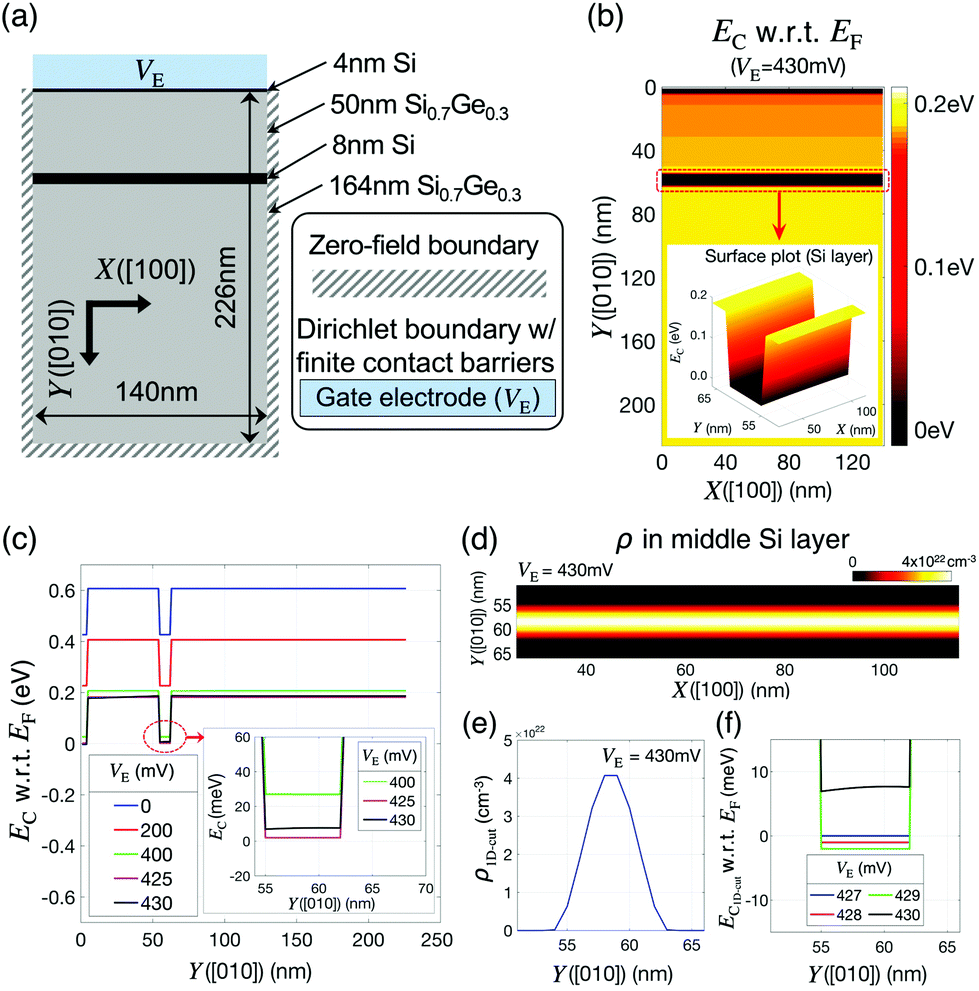 | ||
| Fig. 2 Electrode-driven 2DEG formation. (a) A simulation domain used to investigate the formation of 2D electron gases (2DEG). (b) 2D distribution of the conduction band minimum (EC) that is simulated at VE = 430 mV and T = 1.5 K. (c) Gate controllability of the EC profile at T = 1.5 K. The 1D-cut (along the [010] direction) profiles of EC are presented as a function of the gate biases. (d) Electron distribution in the middle Si layer at VE = 430 mV and T = 1.5 K, and (e) the corresponding 1D-cut profiles along the [010] direction. The results in (d) and (e) clearly indicate a strong confinement of electrons in the middle Si layer along the [010] direction with a peak density of 4 × 1022 cm−3. (f) Effect of electron-filling on EC. Electron-filling in the middle Si layer at VE = 430 mV increases the channel EC due to the screening effect as indicated by the four 1D profiles. | ||
Being injected from 2DEGs under a small electric field imposed along the [100] direction, the electrons could be confined in the channel with appropriate biases of the barrier (VB), left (VL), middle (VM) and right (VR) gate electrodes (Fig. 1(b)). To examine the contribution of these electrodes to electron confinement, we modeled a full charge stability diagram taking VL and VR as control factors, and the details of conductance calculations are available in the ESI.†Fig. 3(a) shows the result obtained at VM = 400 mV and VB = 200 mV, and the shape of the diagram is quite similar to that of the diagram measured for the reported physical DQD structure.8 Being identified with two numbers that show the number of electrons in the left/right QD, the charge states, for the convenience of discussion, are represented with points labeled as P00, P01, P10, and P11. The two control paths for channel initialization to the (1,1) state, which is the starting step of qubit logic operations, are described with white arrows, e.g., P00 → P01 → P11 or P00 → P10 → P11. In the P00 → P01 → P11 path, for example, the state is transferred from (0,0) to (0,1) at VR = 545 mV and VL = 535 mV (indicated with a red arrow), where the ground state energy-level of the right QD touches the EF value that is fixed by the 2DEG reservoirs. The state-transfer from (0,1) to (1,1) then occurs at VR = 555 mV and VL = 546 mV (indicated with a yellow arrow).
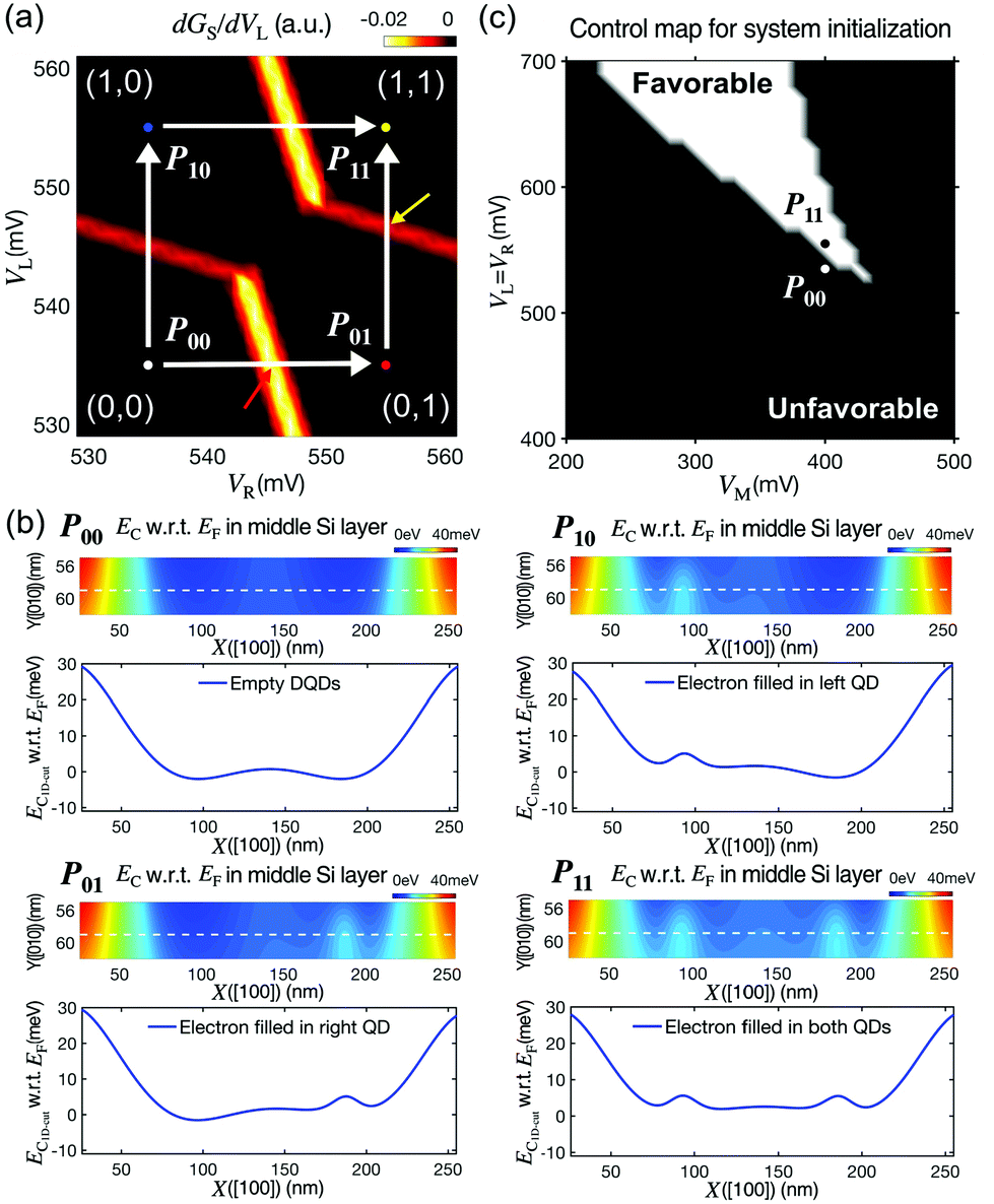 | ||
| Fig. 3 Charge control and qubit initialization. (a) A full charge stability diagram simulated for the target structure at VM = 400 mV and VB = 200 mV. Being in excellent agreement with the diagram measured for the reported device,8 the result shows the four representative charge states (P00, P01, P10, and P11) with two control paths (white arrows) that can be used to initialize the double quantum dot (DQD) system for gate operations. (b) Conduction band minimum (EC) profile at each charge state. Once the channel is initialized to the (1,1) state, the energy valleys are vanished due to the screening effects of the electrons in QDs. (c) Feasibility of the channel initialization represented as a function of (VM, VL = VR). The two biasing points (P00 and P11 state) are included as examples for the clear description of the bias regime where the DQD channel can (white) or cannot be initialized (black). | ||
The electrostatic phenomena at the four charge states are shown in Fig. 3(b), where we present the spatial distribution of EC in the middle Si layer at each charge state with its 1D profile cut along the white dotted line marked in the 2D profile. When the system is at an empty state (P00 at VL = VR = 535 mV), the EC profile has a smooth double-well shape, as VL and VR are higher than VM(= 400 mV). Increasing VL(VR) continuously lowers EC around the left(right) QD when the channel is empty. Once the left(right) QD is filled with an electron (P10(P01) at VL = 555(535) mV and VR = 535(555) mV), however, the channel EC moves up due to the screening effect. When both QDs are filled with an electron (P11 at VL = VR = 555 mV), the EC profile of the middle Si layer no longer shows energy valleys, indicating that the channel has no chances to grab more electrons, which even though can be still injected from 2DEGs. As the stability diagram shown in Fig. 3(a) cannot explain the VM-driven charge control, we provide another diagram in Fig. 3(c), which shows the feasibility of channel initialization as a function of (VM, VL = VR). The two points, which correspond to the P00 and P11 states in Fig. 3(a), are marked as examples to help easy recognition of the bias regime where the channel can (white) or cannot (black) be initialized.
The main role of the middle gate bias VM is to control the barrier height between the two QDs, and the barrier height affects the exchange interaction of the two spin states that are occupied by confined electrons. Representing the coupling strength between the ground down-spin states, the exchange constant (J) acts as a control factor for the generation of quantum entanglement between two spin qubits in a DQD structure. The behavior of J under varying biases thus must be precisely understood. Fig. 4(a) shows the 1D profiles of EC (cut along the white dotted line marked in Fig. 3(b)) simulated at VL = VR = 535 mV and VM = 390–410 mV, where the barrier height is also plotted as a function of VM in the inset figure. Although VL and VR are fixed, increasing VM causes an overall reduction of EC in the middle Si layer. The reduction however is highest near the region below the middle gate; therefore, the barrier height between the two QDs reduces, and the modeling result indicates that the barrier height varies almost linearly and is inversely proportional to VM. As shown in Fig. 4(b), where the charge density profile at the (1,1) state (at VL = VR = 555 mV) is plotted for two different values of VM (400 mV and 405 mV), the reduced barrier height also affects the confinement shape such that the two electrons in the left and right QDs become closer. While VM exerts non-trivial effects on the barrier height (and coupling) between the two spin states, a noticeable change in the Zeeman splitting energy of each state, a critical factor that determines the frequency at which each electron spin resonates, is not observed. The results in Fig. 4(c) show that the Zeeman splitting energy of the ground state in each QD (EZR and EZL) fluctuates within 0.1% of its average in the range of VM, indicating that the resonance frequencies of the two spin states and their coupling strengths can be controlled independently. The sensitivity of J to VM, calculated from the electron distribution in each QD, turns out to be quite high, and hence J increases by ∼30 times with a ΔVM of just 5 mV (Fig. 4(d)) (for those who are interested, we have presented the numerical values of ΔEZR, ΔEZL and ΔJ per unit mV of ΔVM in Table S1 of the ESI†).
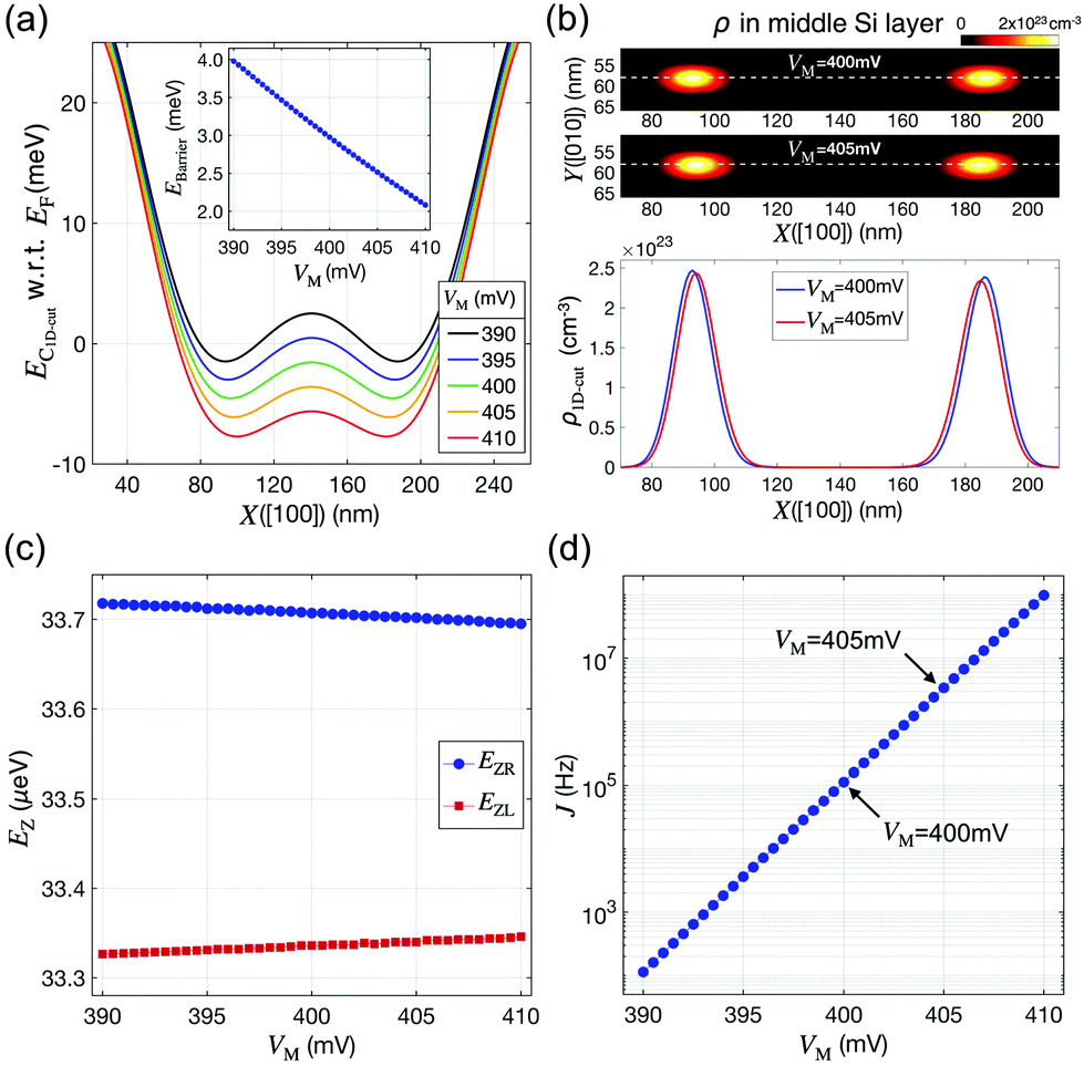 | ||
Fig. 4 Controllability of the middle gate. (a) VM-driven changes of the barrier height between double quantum dots (DQDs). VL and VR are set to 535 mV, and VM is varied from 390 to 410 mV with a 5 mV step. The barrier height (ΦB) drops almost linearly with increasing VM, and  is about −0.1 eV V−1. (b) Charge density profiles in the channel at the (1,1) state, and they are obtained for two values of VM (at VR = VR = 555 mV). Increasing VM not only reduces ΦB but also makes the two electrons confined in the DQD channel become closer. (c) Sensitivity of the Zeeman splitting energy (EZ) and (d) exchange energy (J) to VM. EZ of the ground states in each QD (EZR and EZL) does not show any noticeable dependence on VM. But the J values of the two confined electrons exponentially grow with increasing VM. This huge difference in the sensitivity implies that the resonance and entanglement of two electron spins can be controlled independently. is about −0.1 eV V−1. (b) Charge density profiles in the channel at the (1,1) state, and they are obtained for two values of VM (at VR = VR = 555 mV). Increasing VM not only reduces ΦB but also makes the two electrons confined in the DQD channel become closer. (c) Sensitivity of the Zeeman splitting energy (EZ) and (d) exchange energy (J) to VM. EZ of the ground states in each QD (EZR and EZL) does not show any noticeable dependence on VM. But the J values of the two confined electrons exponentially grow with increasing VM. This huge difference in the sensitivity implies that the resonance and entanglement of two electron spins can be controlled independently. | ||
Once EZR, EZL and J at the (1,1) state are known with device simulations as discussed so far, the time responses of the electron spin qubits in the DQD system can be predicted by solving a time-dependent Schrödinger equation that is established with the Heisenberg Hamiltonian of two neighboring spins.28 Here, we chose the real-time 1-qubit NOT logic operation as a modeling target, and to control the electron spin resonance (ESR) in the QDs, a dynamic magnetic field BY, whose amplitude and frequency were user-defined factors, was assumed to be applied along the [010] direction. As addressed, the starting step of the qubit logic operations was the initialization of the DQD system, following which the ground down-spin state of each QD (|↓〉L and |↓〉R) was filled with a single electron. For this purpose, the system was simulated at VL = VR = 555 mV. VM was set to 400 mV to lead both QDs to perform independent 1-qubit operations with a weak correlation. In a 2-qubit frame, this initial state was represented with |↓↓〉 = |↓〉L ⊗ |↓〉R, where the symbol ‘⊗’ indicates a tensor-product operation. Fig. 5(a) and (b) show the corresponding 2-qubit time responses when the drive frequency of BY is set equal to the Zeeman splitting energies EZL (8.045 GHz) and EZR (8.134 GHz), respectively. When the frequency is 8.045 GHz, ESR occurs only in the left QD, and the spin qubit in the right QD remains unchanged from its initial down-spin state. Among the time responses of the four 2-qubit states in Fig. 5(a), therefore, only the two cases (|↑↓〉 and |↓↓〉), where the right qubit is |↓〉, show a Rabi oscillation. Likewise, at a frequency of 8.134 GHz that drives ESR only in the right QD, the oscillation was observed only in the time response of |↓↑〉 and |↓↓〉, as shown in Fig. 5(b). In both cases, a NOT logic operation was achieved when the probability of a specific output satisfied a certain condition. If ESR occurs only in the left QD (Fig. 5(a)), for example, a NOT logic operation can be achieved at all the time spots where P(|↑↓〉) (the probability that a |↑↓〉 state is measured) becomes 1.
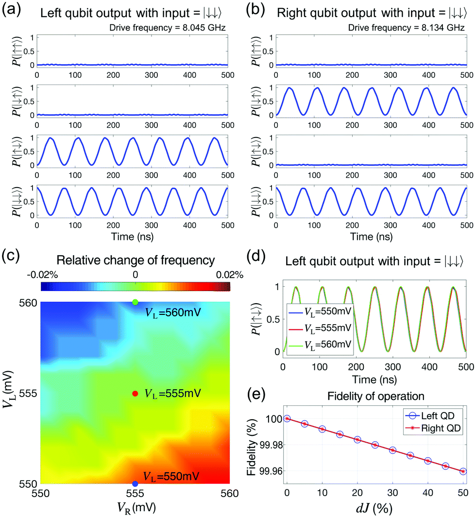 | ||
| Fig. 5 NOT logic operations under noises in control signals. (a) and (b) Two-qubit time responses of the double quantum dot (DQD) system under an AC magnetic field whose drive frequency is set to 8.045 GHz and 8.134 GHz. The system is initialized with VL = VR = 555 mV and VM = 400 mV. At a frequency of 8.045 GHz where the electron spin resonance (ESR) is observed only in the left QD, for example, a NOT operation is achieved at time spots when the probability that a |↑↓〉 state is measured (P(|↑↓〉)) becomes 1. (c) The ESR frequency of the left QD ground state shown as a function of (VL, VR) at VM = 400 mV. (d) Time responses of a |↑↓〉 state at a frequency of 8.045 GHz and ΔVR = ±5 mV. (e) The fidelity of the first NOT operation shown as a function of the variation in the exchange constant (dJ). Results in (c)–(e) reveal that the ESR frequency is quite independent of the shape of the QD potential, even though the system is under a magnetic field with a spatial gradient, and support the robustness of 1-qubit operations against the noise of input signals. | ||
Though we chose a bias point of VL = VR = 555 mV and VM = 400 mV to initialize the DQD channel, other (VL, VR) biases at VM = 400 mV, in principle, must be also available for the same purpose as long as they belong to the top-right regime in the stability diagram (Fig. 3(a)). However, if these DC bias points and the resulting ESR frequencies of the QDs are strongly correlated, the complexity in controlling the logic operations would increase. A modeling result of the corresponding correlation is shown in Fig. 5(c), where we plotted the relative variation of the drive frequency in the left QD as a function of (VL, VR). The frequency driven at VL = VR = 555 mV and VM = 400 mV is taken as a reference. With ΔVL and ΔVR at ≤5 mV, the maximum deviation of the frequency turns out to be under 0.02% of its reference value, and this deviation is more sensitive to ΔVL than ΔVR since the confinement of the left QD is affected more strongly by the left gate electrode than the right one (detailed dataset for the variation of ESR frequencies per unit mV of ΔVL and ΔVR is available with the corresponding valley-splitting energies in Tables S2 and S3 of the ESI†). The time responses of a |↑↓〉 state with ΔVL of ±5 mV are plotted in Fig. 5(d). Even though the frequency deviation driven by ΔVL is extremely small, the resulting phase-shift keeps being accumulated, and remarkable changes may be driven in the response as time elapses. However, up to ∼500 ns, the change in P(|↑↓〉) measured does not become noticeable (≪1%). The robustness of the logic operations against the unintentional inaccuracy in VL can be also explained with the modeling results. Assuming that the input bias has an uncertainty of ∼1 mV under the experimental conditions, we observed that the fidelity of the first NOT operation (at 34.5 ns) dropped by less than 0.2%. The fidelity is also depicted as a function of the unexpected deviation of J (dJ) in Fig. 5(e), which shows a fidelity of 99.96% even at dJ of 50%. Considering that J doubles up with the ΔVM of 1 mV (Fig. 4(d)), we conclude that 1-qubit operations in the target DQD system, represented by a NOT operation, are reasonably robust against the noise of input signals.
All the modeling results discussed so far assumed a perfect symmetry in relation to the device geometry. However, a perfectly symmetric DQD structure may not be always guaranteed in the real world scenario due to unintentional lithographical errors. Although the geometric symmetry can be broken by a variety of physical features, including non-uniform compositions in SiGe layers and surface and interface roughnesses, to explore the connection between the broken symmetry and device functionality, here we only focus on the case wherein the left and right gate electrodes have different sizes. As Fig. 6(a) shows, this size mismatch is introduced in the simulation domain with two variables (ΔWL and ΔWR) that also affect the size of the middle gate electrode. In spite of the broken symmetry observed in the DQD potential profile at VL = VR = 555 mV and VM = 400 mV, its effect on the major factors that determine 1-qubit logic operations turned out not to be quite remarkable in the considered range of (ΔWL, ΔWR). In Fig. 6(b), we show the 1D-cuts of the electron density profiles (along the [100] direction in the center of the middle Si layer) and the corresponding variations in J for four cases (ΔWL = ±4 nm and ΔWR = ±4 nm). Even with a size-mismatch of 4 nm corresponding to ∼7% of the reference size of the electrodes, the dJ value led by the change in the electron density profile stays under 2% with respect to the symmetric case. The Zeeman splitting energy (ESR frequency) of each QD is shown in Fig. 6(c) and (d) as a function of ΔWL and ΔWR, respectively, and the results indicate that the relative change in the frequencies is less than just 0.03% at a size mismatch of 4 nm, implying the robustness of the logic operations.
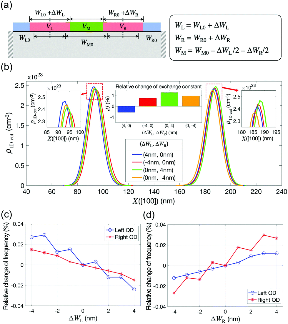 | ||
| Fig. 6 Effects of the electrode-driven geometric asymmetry. (a) A conceptual illustration showing how the size mismatch between the left and right gate electrodes is incorporated into the simulation domain. Note that ΔWL and ΔWR also affect the size of the middle gate electrode. (b) Electron density profiles (cut along the [100] direction in the center of the middle Si layer) and the corresponding changes of the exchange constant (dJ) with respect to the symmetric case (VL = VR = 555 mV, VM = 400 mV). (c) and (d) ESR frequencies as a function of ΔWL and ΔWR. Since even a 4 nm size mismatch between the two electrodes (6.7% of the size of electrodes in the symmetric case) drives |dJ| < 2% and changes the frequency <0.03% against the symmetric case, the robustness of the logic operations can be understood to be strong against the geometric asymmetry driven by electrodes. | ||
4 Conclusion
Electron spin quantum bits (qubits) in electrode-driven Si double quantum dot (DQD) structures were elaborately examined from the perspective of device design with a systematic modeling approach based on a hybrid utilization of the semi-classical and quantum mechanical theory. Through rigorous simulations of a recently realized DQD structure,8 we discussed the designs of electrode-driven electron reservoirs and derived a full stability diagram which nicely reproduced the experimentally measured charge controls, validating the modeling approach. After quantifying the range of DC control biases that led the system to be ready for quantum logic operations, we found that the Zeeman splitting energy (EZ) of the spin states, which determines the resonance frequency of spin qubits, was not quite sensitive to bias-driven changes in the confinement potentials even under a spatially varying magnetic field, thereby theoretically confirming that EZ and the exchange interaction between two neighboring spin states (J) could be manipulated independently in real DQD systems. The effects of non-ideal factors on the quality of the gate devices were also investigated by the modeling of limited cases, and the results showed the robustness of real-time NOT logic operations under variations in the control signals and sizes of the gate electrodes. Though this work is still in progress, since it does not yet include a rigorous discussion on multi-qubit logic operations involving quantum entanglement, the engineering details we delivered at this preliminary stage already presented sound design clues, indicating the practicality of our systematic modeling approach that is hard to replace with full quantum mechanical simulations.Conflicts of interest
There are no conflicts to declare.Acknowledgements
This research has been carried as the Korea Institute of Science and Technology Information (KISTI) institutional R&D program (K-20-L02-C09) and has been supported by a grant from the National Research Foundation of Korea (NRF-2020M3E4A1079792) and the Institute for Information & Communications Technology Promotion (2019-0-00003) funded by the Korea government (MSIP). HR appreciates Jeehye Sohn for all the support and encouragement for this research.References
- L. Gaudreau, G. Granger, A. Kam, G. C. Aers, S. A. Studenikin, P. Zawadzki, M. Pioro-Ladrière, Z. R. Wasilewski and A. S. Sachrajda, Nat. Phys., 2012, 8, 54–58 Search PubMed.
- J. M. Nichol, L. A. Orona, S. P. Harvey, S. Fallahi, G. C. Gardner, M. J. Manfra and A. Yacoby, npj Quantum Inf., 2017, 3, 3 Search PubMed.
- B. Maune, M. Borselli, B. Huang, T. Ladd, P. Deelman, K. Holabird, A. Kiselev, I. Alvarado-Rodriguez, R. Ross, A. Schmitz, M. Sokolich, C. Watson, M. Gyure and A. Hunter, Nature, 2008, 481, 344–347 CrossRef PubMed.
- Z. Shi, C. B. Simmons, J. R. Prance, J. K. Gamble, T. S. Koh, Y. Shim, X. Hu, D. E. Savage, M. G. Lagally, M. A. Eriksson, M. Friesen and S. N. Coppersmith, Phys. Rev. Lett., 2012, 108, 140503 CrossRef PubMed.
- J. Gorman, D. G. Hasko and D. A. Williams, Phys. Rev. Lett., 2005, 95, 090502 CrossRef CAS PubMed.
- M. Veldhorst, J. C. C. Hwang, C. H. Yang, A. W. Leenstra, B. de Ronde, J. P. Dehollain, J. T. Muhonen, F. E. Hudson, K. M. Itoh, A. Morello and A. S. Dzurak, Nat. Nanotechnol., 2014, 9, 981–985 CrossRef CAS PubMed.
- M. Veldhorst, C. H. Yang, J. C. C. Hwang, W. Huang, J. P. Dehollain, J. T. Muhonen, S. Simmons, A. Laucht, F. E. Hudson, K. M. Itoh, A. Morello and A. S. Dzurak, Nature, 2015, 526, 410–414 CrossRef CAS PubMed.
- D. M. Zajac, A. J. Sigillito, M. Russ, F. Borjans, J. M. Taylor, G. Burkard and J. R. Petta, Science, 2018, 26, 439–442 CrossRef PubMed.
- T. F. Watson, S. G. J. Philips, E. Kawakami, D. R. Ward, P. Scarlino, M. Veldhorst, D. E. Savage, M. G. Lagally, M. Friesen, S. N. Coppersmith, M. A. Eriksson and L. M. K. Vandersypen, Nature, 2018, 555, 633–637 CrossRef CAS PubMed.
- C. H. Yang, R. C. C. Leon, J. C. C. Hwang, A. Saraiva, T. Tanttu, W. Huang, J. C. Lemyre, K. W. Chan, K. Y. Tan, F. E. Hudson, K. M. Itoh, A. Morello, M. Pioro-Ladrière, A. Laucht and A. S. Dzurak, Nature, 2020, 580, 350–354 CrossRef CAS.
- L. Szolnoki, A. Kiss, B. Dóra and F. Simon, Sci. Rep., 2017, 7, 9949 CrossRef PubMed.
- M. Usman, Y.-H. Tan, H. Ryu, S. S. Ahmed, H. J. Krenner, T. B. Boykin and G. Klimeck, Nanotechnology, 2011, 22, 315709 CrossRef.
- E. Ferraro and E. Prati, Phys. Lett. A, 2020, 1–8 Search PubMed , (in press).
- F. A. Zwanenburg, A. S. Dzurak, A. Morello, M. Y. Simmons, L. C. L. Hollenberg, G. Klimeck, S. Rogge, S. N. Coppersmith and M. A. Eriksson, Rev. Mod. Phys., 2013, 85, 961 CrossRef CAS.
- J. T. Muhonen, J. P. Dehollain, A. Laucht, F. E. Hudson, R. Kalra, T. Sekiguchi, K. M. Itoh, D. N. Jamieson, J. C. McCallum, A. S. Dzurak and A. Morello, Nat. Nanotechnol., 2014, 9, 986–991 CrossRef CAS.
- R. Maurand, X. Jehl, D. Kotekar-Patil, A. Corna, H. Bohuslavskyi, R. Laviéville, L. Hutin, S. Barraud, M. Vinet, M. Sanquer and S. Franceschi, Nat. Commun., 2016, 7, 13575 CrossRef CAS PubMed.
- V. Mazzocchi, P. Sennikov, A. Bulanov, M. Churbanov, B. Bertrand, L. Hutin, J. Barnes, M. Drozdov, J. Hartmann and M. Sanquer, J. Cryst. Growth, 2019, 509, 1–7 CrossRef CAS.
- N. Abrosimov, D. Aref'ev, P. Becker, H. Bettin, A. Bulanov, M. Churbanov, S. Filimonov, V. Gavva, O. Godisov, A. Gusev, T. Kotereva, D. Nietzold, M. Peters, A. Potapov, H.-J. Pohl, A. Pramann, H. Riemann, P.-T. Scheel, R. Stosch, S. Wundrack and S. Zakel, Metrologia, 2017, 54, 599–609 CrossRef CAS.
- Y.-C. Yang, S. N. Coppersmith and M. Friesen, npj Quantum Inf., 2019, 5, 12 CrossRef.
- R. Wang, R. S. Deacon, J. Sun, J. Yao, C. M. Lieber and K. Ishibashi, Nano Lett., 2019, 19, 1052–1060 CrossRef PubMed.
- E. Kawakami, T. Jullien, P. Scarlino, D. R. Ward, D. E. Savage, M. G. Lagally, V. V. Dobrovitski, M. Friesen, S. N. Coppersmith, M. A. Eriksson and L. M. K. Vandersypen, Proc. Natl. Acad. Sci. U. S. A., 2016, 113, 11738–11743 CrossRef CAS PubMed.
- J. J. Burnett, A. Bengtsson, M. Scigliuzzo, D. Niepce, M. Kudra, P. Delsing and J. Bylander, npj Quantum Inf., 2019, 5, 54 CrossRef.
- D. Loss and D. P. DiVincenzo, Phys. Rev. A, 1998, 57, 120 CrossRef CAS.
- V. Grimalsky, L. M. Gaggero-Sager and S. Koshevaya, Phys. B, 2011, 406, 2218–2223 CrossRef CAS.
- J. Wang, A. Rahman, A. Ghosh, G. Klimeck and M. Lundstrom, IEEE Trans. Electron Devices, 2005, 52, 1589–1595 CrossRef.
- Y. Nosho, Y. Ohno, S. Kishimoto and T. Mizutani, Nanotechnology, 2006, 17, 3412–3415 CrossRef CAS PubMed.
- R. Neumann and L. R. Schreiber, J. Appl. Phys., 2015, 117, 193903 CrossRef.
- M. Russ, D. M. Zajac, A. J. Sigillito, F. Borjans, J. M. Taylor, J. R. Petta and G. Burkard, Phys. Rev. B: Condens. Matter Mater. Phys., 2018, 97, 085421 CrossRef CAS.
- R. A. Jabr, M. Hamad and Y. Mohanna, Int. J. Electr. Eng. Educ., 2007, 44, 23–33 CrossRef.
Footnotes |
| † Electronic supplementary information (ESI) available. See DOI: 10.1039/D0NR05070A |
| ‡ These authors contributed equally to this work. |
| This journal is © The Royal Society of Chemistry 2021 |