
Surface-induced phase engineering and defect passivation of perovskite nanograins for efficient red light-emitting diodes†
Yong-Chun
Ye
a,
Yanqing
Li
*b,
Yu
Tian
a,
Xiao-Yi
Cai
a,
Yang
Shen
a,
Kong-Chao
Shen
a,
Xingyu
Gao
 c,
Fei
Song
c,
Wenjun
Wang
d and
Jian-Xin
Tang
*ae
c,
Fei
Song
c,
Wenjun
Wang
d and
Jian-Xin
Tang
*ae
aInstitute of Functional Nano & Soft Materials (FUNSOM), Jiangsu Key Laboratory for Carbon-Based Functional Materials & Devices, Soochow University, Suzhou 215123, China. E-mail: jxtang@suda.edu.cn
bSchool of Physics and Electronics Science, Ministry of Education Nanophotonics and Advanced Instrument Engineering Research Center, East China Normal University, Shanghai 200062, China. E-mail: yqli@phy.ecnu.edu.cn
cShanghai Synchrotron Radiation Facility, Zhangjiang Laboratory, Chinese Academy of Sciences, Shanghai, 201204, China
dSchool of Physical Science and Information Technology, Shandong Provincial Key Laboratory of Optical Communication Science and Technology, Liaocheng University, Shandong 252059, China
eInstitute of Organic Optoelectronics (IOO) Jiangsu Industrial Technology Research Institute (JITRI), Wujiang, Suzhou 215215, Jiangsu, China
First published on 8th December 2020
Abstract
Organic–inorganic hybrid lead halide perovskites are potential candidates for next-generation light-emitting diodes (LEDs) in terms of tunable emission wavelengths, high electroluminescence efficiency, and excellent color purity. However, the device performance is still limited by severe non-radiative recombination losses and operational instability due to a high degree of defect states on the perovskite surface. Here, an effective surface engineering method is developed via the assistance of guanidinium iodide (GAI), which allows the formation of surface-2D heterophased perovskite nanograins and surface defect passivation due to the bonding with undercoordinated halide ions. Efficient and stable red-emission LEDs are realized with the improved optoelectronic properties of GAI-modified perovskite nanograins by suppressing the trap-mediated non-radiative recombination loss. The champion device with a high color purity at 692 nm achieves an external quantum efficiency of 17.1%, which is 2.3 times that of the control device. Furthermore, the operational stability is highly improved, showing a half-lifetime of 563 min at an initial luminance of 1000 cd m−2. The proposed GAI-assisted surface engineering is a promising approach for defect passivation and phase engineering in perovskite films to achieve high-performance perovskite LEDs.
1. Introduction
In recent years, metal halide perovskites have been emerging as a promising semiconductor material for solar cells,1–6 light-emitting diodes (LEDs),7–14 photodetectors,15,16 lasers,17 and so on. Perovskite LEDs (PeLEDs) have attracted considerable attention because of their tunable emission wavelength, high photoluminescence quantum yield, excellent color purity, etc.14 The external quantum efficiency (EQE) of PeLEDs with green, red, or near-infrared emission has exceeded 20% through defect passivation,10,11,18 morphology control,19,20 dimensionality tuning,21 interface engineering,22–24 and a light-outcoupling scheme.18,25Regardless of the rapid progress made in PeLEDs, the device performance and stability are still limited by many extrinsic factors (e.g., moisture, heat and light) and intrinsic defects in solution-processed perovskite films (e.g., halide dangling bonds formed by cation vacancies and interstitial halides, or undercoordinated lead defects related to halide vacancies and interstitial lead). Consequently, severe ion migrations and non-radiative recombination losses hinder the development of PeLEDs. Lewis bases with a lone pair were commonly employed to reduce the density of lead defects, such as amine (–NH2),26,27 carbonyl (C![[double bond, length as m-dash]](https://www.rsc.org/images/entities/char_e001.gif) O),28 carboxyl (–COOH),29 and phosphine oxide (PO).23 In addition, Lewis acids with an ammonium group can form strong hydrogen bonds with halide ions to passivate the halide anions of the [PbX6]4− octahedra.
O),28 carboxyl (–COOH),29 and phosphine oxide (PO).23 In addition, Lewis acids with an ammonium group can form strong hydrogen bonds with halide ions to passivate the halide anions of the [PbX6]4− octahedra.
In contrast to the incorporation of suitable passivation additives in perovskite precursors, the surface-induced secondary growth technique has been introduced to achieve efficient and stable perovskite optoelectronic devices. For example, in the field of perovskite solar cells, Zhu and co-workers introduced a secondary growth technique with guanidinium bromide for the formation of a more n-type perovskite film on top of the three-dimensional (3D) perovskite bulk film, leading to the enhanced photovoltage and mitigated non-radiative recombination.5 In addition, such a secondary growth strategy can lead to the formation of an ultrathin two-dimensional (2D) Ruddlesden–Popper layered structure, which has a significant impact on the morphology and photophysical properties of perovskite films.4 However, the secondary growth technique usually used in solar cells induces the evolution of large-sized crystal grains, which inevitably mitigate the charge confinement and decrease the exciton binding energy in perovskite films. Therefore, it is critical to form small-sized perovskite grains (<100 nm) for effective exciton/charge carrier confinement to facilitate the radiative recombination in PeLEDs.19,30–32 At the same time, small crystal grains with a large surface-to-volume ratio usually bring about a high degree of surface defect states in perovskite films. To achieve high efficiencies in PeLEDs, it is thus indispensable to explore an effective means of surface treatment, which can mitigate such drawbacks by controlling the perovskite nanograins with small sizes and low surface defect density simultaneously. In addition, the formation of a multidimensional perovskite interface can boost the carrier transfer at the interface, and thus enhance the radiative recombination.
In this work, we report one method to reconstruct the top surface of perovskite films via the assistance of solution-processed guanidinium iodide (GAI), enabling both surface passivation and secondary grain growth. The morphological and crystal characterization confirm the formation of 2D/3D multidimensional perovskites. Optical measurements prove the improved optoelectronic properties of perovskite films due to the passivation of surface defects through hydrogen bonding interactions between GA+ ions and halide vacancies. As a result, efficient and stable red-emission LEDs are realized by suppressing the trap-mediated non-radiative recombination losses, leading to a peak EQE of 17.1% at an emission wavelength of 692 nm. Moreover, the targeted device exhibits improved operational stability with a largely prolonged half-lifetime (T50) of 563 min at an initial luminance of 1000 cd m−2.
2. Experimental section
2.1. Materials
Formamidinium iodide (FAI) and formamidinium bromide (FABr) were purchased from Greatcell Solar. Lead(II) bromide/iodide (PbI2/PbBr2), cesium iodide (CsI), 5-Aminovaleric Acid (5AVA), and 2-methoxyethanol were purchased from TCI. Guanidine hydroiodide (GAI) was purchased from J&K. Poly[(9,9-dioctylfluorenyl-2,7-diyl)-alt-(4,4′-(N-(4-butylphenyl))diphenylamine)] (TFB) was purchased from Dyesol. Dimethyl sulfoxide (DMSO), zinc acetate, and molybdenum(VI) oxide (MoO3) were purchased from Alfa Aesar. Dimethylformamide (DMF) and polyethylenimine, 80% ethoxylated solution (PEIE) were purchased from Sigma Aldrich. m-Xylene (99% extra dry) was purchased from Acros. Ethanol and isopropanol (IPA) were purchased from Aladdin. All the chemical materials were directly used without any further purifications. The perovskite precursor solution was prepared by dissolving FAI (7 mg), FABr (6 mg), CsI (26 mg), PbI2 (46 mg), PbBr2 (0.13 mg), and 5AVA (6 mg) in 1 mL of the mixed solvent (DMF![[thin space (1/6-em)]](https://www.rsc.org/images/entities/char_2009.gif) :DMSO = 4:1 in volume), and was stirred at 60 °C for 2 h in a N2-filled glovebox.
:DMSO = 4:1 in volume), and was stirred at 60 °C for 2 h in a N2-filled glovebox.
2.2. Device fabrication
The patterned indium-tin-oxide (ITO) coated glass substrates were used as the anode, and were sequentially sonicated with detergent, acetone, ethanol and isopropanol for 10 min, and finally treated with ultraviolet-ozone for 15 min. The zinc oxide (ZnO) nanocrystal solution was spin-coated on ITO at 4000 rpm for 40 s, followed by thermal annealing in air at 150 °C for 15 min. Then, a PEIE layer was prepared by spin-coating the PEIE solution in 2-methoxyethanol (0.4 wt%) onto ZnO nanocrystals, and was annealed in air at 150 °C for 10 min. The as-prepared ITO/ZnO/PEIE substrates were transferred into a N2-filled glovebox, in which the perovskite layer was prepared on the ITO/ZnO/PEIE substrates by spin-coating the precursor solution by a two-step process at 1000 rpm for 5 s and at 4000 rpm for 55 s and then annealing at 100 °C for 30 min. In the post-treatment process, GAI was dissolved in IPA (5 mM) and spin-coated onto the perovskite surface at 4000 rpm without any further processing. The hole-transport layer was prepared by spin-coating 50 μL of the TFB m-xylene solution (8 mg mL−1) onto the perovskite film. Finally, the samples were transferred to an interconnected high-vacuum deposition system (base pressure < 4 × 10⁻⁷ Torr) for the thermal evaporation of MoO3 and Al through shadow masks to achieve the device. The device area was determined to be 10 mm2.2.3. Property characterization
Morphologies of the perovskite films were characterized by scanning electron microscopy (SEM) (Zeiss Supra 55) and atomic force microscopy (AFM) (Veeco Multimode V) in the tapping mode. Grazing-incidence X-ray diffraction (GIXRD) measurements were performed at the BL14B1 beamline of the Shanghai Synchrotron Radiation Facility (SSRF) using an X-ray beam at a wavelength of 1.2398 Å. The absorption spectra were characterized with a UV/vis/near-IR spectrometer with an integrating-sphere accessory (PerkinElmer Lambda 950). The steady-state photoluminescence (PL) spectra and transient PL decays of the perovskite films were recorded with a Quantaurus-Tau fluorescence lifetime spectrometer (C11367-32, Hamamatsu Photonics). Low-temperature measurements were conducted using a cryostat (Oxford Optistat DN). Ultraviolet photoemission spectroscopy (UPS) was performed with a Kratos AXIS UltraDLD ultrahigh vacuum (UHV) surface analysis system with an unfiltered He I (21.2 eV) lamp at a total instrumental energy resolution of 100 meV. The current density–voltage–luminance (I–V–L) characteristics and electroluminescence (EL) spectra of the PeLEDs were measured simultaneously with a computer-controlled programmable power source (Keithley model 2400) and a luminance meter/spectrometer (PhotoResearch PR670) in an air ambience at room temperature. Angular EL measurements were conducted by rotating the sample stage. The EQEs were calculated by taking a full account of the measured I–V–L characteristics and the EL spectra of the PeLEDs with a Lambertian profile. The lifetime of the PeLEDs that were encapsulated in a glass lid and epoxy resin was measured using a 64 channel ZJLS-4 type OLED life aging testing system in the constant current mode at room temperature.3. Results and discussion
Fig. 1a depicts the GAI-assisted surface treatment, in which the mixed-cation lead mixed-halide perovskite film was firstly prepared using a nonstoichiometric amount of FAxCs1−xPb(IyBr1−y)3 (FA: formamidinium),27 and then passivated by spin-coating the isopropanol solution containing guanidinium iodide onto the perovskite surface (see the details in the Experimental section). Fig. 1b shows the scanning electron microscopy (SEM) images of the control and GAI-modified perovskite films. The control film shows round shapes with irregular clusters, which are randomly tiled on the substrate. After the GAI-assisted surface treatment with various GAI concentrations, the morphology of the perovskite film underwent a significant change (Fig. S1†). Notably, the produced small grains are attached to big perovskite grains to reorganize more uniform grain sizes in the GAI-modified perovskite film (Fig. S2†). Atomic force microscopy (AFM) measurements confirm the increase of the crystal size with the surface treatment process (Fig. S3†). Meanwhile, the film colors changed from brownish yellow (the control sample) to brownish red (the GAI-modified sample) as shown in Fig. S2.† The grazing incidence X-ray diffraction (GIXRD) analysis was conducted to examine the crystal structures of the control and GAI-modified perovskite films. The (100), (110), and (200) crystal planes are clearly shown in Fig. 1c, and are generally recognized as three-dimensional (3D) perovskites. Moreover, the (100) crystal plane is preferably oriented to the perpendicular substrate. Notably, the emergence of two-dimensional (2D) phases can be distinctly observed in the low qz-value diffraction pattern of the GAI-modified perovskite film (Fig. 1c).33,34 In order to exclude the effect of GAI, GIXRD measurements on the pure GAI film were conducted (Fig. S4†). The q curves related to the diffraction intensity of the perovskite films extracted from the GIXRD pattern provide intuitive evidence that GAI does not exist in the perovskite film. In addition, the absorption transition at 515 nm occurs upon the surface treatment with increasing GAI concentrations (Fig. 2a), indicating that the GAI modification can lead to the formation of 2D FAGAPbI4 on the surface of bulky 3D perovskite grains.35,36 Moreover, the absorption transition at 515 nm shows an enhanced intensity with increasing GAI concentration, while the overall light absorbance shows a decrease in the intensity, implying that more 2D phase perovskites are formed. The absorption spectrum of GAI shows that an absorption transition at 515 nm was not observed (Fig. S5†), which further proves the formation of 2D phases on the surface of the GAI-modified perovskite. It is thus inferred that the GAI-assisted surface treatment on the perovskite layer results in the reorganization of the crystal grains and the formation of surface-2D/bulk-3D heterophased perovskites. | ||
| Fig. 1 Morphologies and crystal structures via surface defect passivation. (a) Schematic illustration of the fabrication of pristine and GAI (5 mM)-modified perovskite thin films. (b) Top-view SEM images of the control and GAI-modified perovskite films. (c) GIXRD patterns of the control and GAI-modified perovskite films. | ||
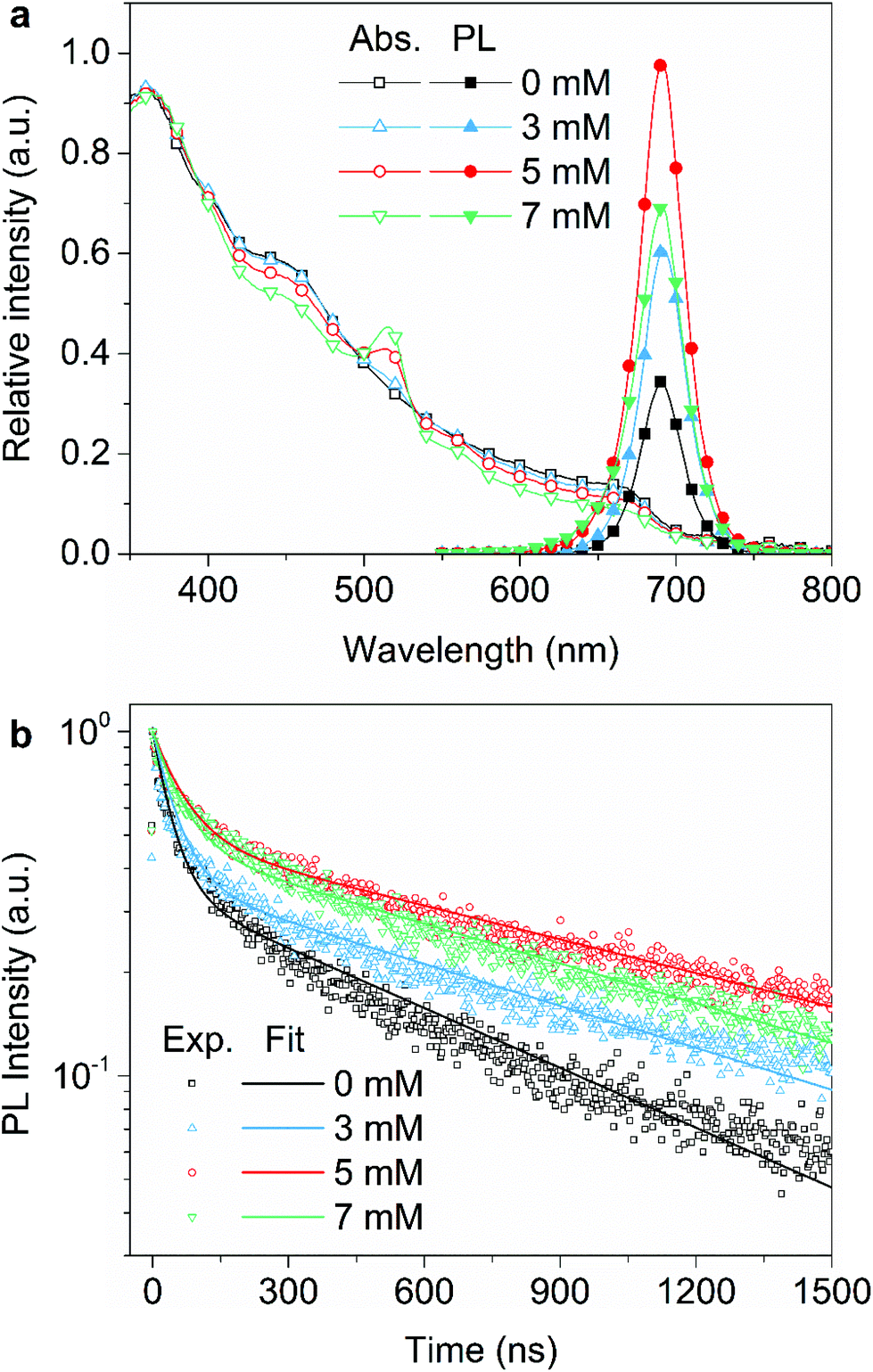 | ||
| Fig. 2 Optical characterization of perovskite films treated with various GAI concentrations. (a) Absorption spectra (the hollow symbol) and PL spectra (the solid symbol). (b) TRPL decay profiles (the hollow symbol) at 692 nm under 373 nm excitation. The TRPL curves are fitted with a bi-exponential decay function (the solid line). | ||
The optical properties of the perovskite films modified with various GAI concentrations are shown in Fig. 2. The GAI-modified perovskite films exhibit enhanced photoluminescence (PL) intensities, and the maximum emission is achieved at an optimal GAI concentration of 5 mM (Fig. 2a). The temperature-dependent PL spectra show a significant increase in the intensity with the temperature decreasing from 300 K to 80 K, while the peak positions remain almost constant (Fig. S6†). Furthermore, the time-resolved PL (TRPL) decays were used to evaluate the exciton decay dynamics in the perovskite films. The prolonged PL lifetimes with increasing GAI concentration were observed (Fig. 2b). A bi-exponential decay function was used to fit the TRPL curves,20 and the TRPL decay shows fast (τ1 = 67 ns) and slow (τ2 = 1330 ns) carrier lifetimes at the optimal GAI concentration, whereas the control perovskite exhibits TRPL lifetimes of τ1 = 40 ns and τ2 = 750 ns. The longer lifetime of the photoluminescence transition for the GAI-modified perovskite film provides direct evidence of the decrease in the concentration of the defects (Table S1†). The average PL lifetime (τavg) is determined to be 686 ns at a GAI concentration of 5 mM, which is 2-fold greater than that of the control film (289 ns). The decrease in both PL intensity and PL lifetime at a GAI concentration of 7 mM might be caused by the formation of too many 2D-phases in the perovskite films as observed in Fig. 2a. Nevertheless, the strong PL intensity and long PL lifetime suggest that the surface defects have been effectively reduced in the GAI-modified perovskite films, resulting in the significant suppression of the trap-mediated non-radiative monomolecular recombination. It has been reported that the surface defect passivation of halide perovskites may be related to the interaction between surface agents and incomplete PbX64− octahedra.23 To verify this possibility, Fourier transform infrared (FTIR) spectroscopy measurements were conducted. As shown in Fig. S7,† the N–H and CN bond absorption peaks assigned to GAI can also be found in the GAI-modified perovskite film, confirming the existence of GA+ ions in the perovskite film. Moreover, the relative shifts of these peaks are observed in the GAI-modified perovskite film, implying the possible bonding between the GA+ ions and perovskite grains.12,33
The results mentioned above indicate that the GAI-assisted surface treatment has a positive impact on the crystal reorganization and defect passivation of the perovskite films. To further confirm these effects, PeLEDs without and with GAI modification were fabricated. Fig. 3a displays the device architecture adopted in this study, which shows a structure of ITO/ZnO (∼35 nm)/PEIE/perovskite (∼30 nm)/TFB (30 nm)/MoOx (7 nm)/Al (100 nm). Here, indium tin oxide (ITO) was used as a cathode, polyethylenimine ethoxylated (PEIE)-modified zinc oxide (ZnO) nanocrystals as an electron-transport layer (ETL), Poly[(9,9-dioctylfluorenyl-2,7-diyl)-alt-(4,4′-(N-(4-butylphenyl))diphenylamine)] (TFB) as a hole-transport layer (HTL), and molybdenum oxide (MoOx)/Al as a bilayer anode. The layer thickness was estimated from the cross-sectional SEM image as shown in Fig. 3a. The normalized electroluminescence (EL) spectra of the PeLEDs are shown in Fig. 3b, showing a deep red emission peak at 692 nm with a narrow full-width at half-maximum (FWHM) of 32 nm. The inset of Fig. 3b shows a photograph of the PeLED operating at 3 V. The corresponding Commission Internationale de I'Eclairage (CIE) chromaticity coordinates of these devices are (0.71, 0.27), revealing a red emission with high color purity (Fig. 3c). It is also noted that the EL spectra under various bias voltages are very stable except for a slight red-shift to 694 nm of the device at a GAI concentration of 7 mM (Fig. S8†), indicating no phase segregation under electrical stress. Their angular emission intensities are close to an ideal Lambertian profile, and the corresponding EL spectra showed no perceivable change at different viewing angles (Fig. S9†).
 | ||
| Fig. 3 Device structure and performance of red PeLEDs without and with GAI modification. (a) Schematic illustration of the device architecture and cross-section SEM image. (b) Normalized EL spectra. The inset shows a photograph of the GAI-modified PeLED under operation. (c) The corresponding Commission Internationale de I'Eclairage (CIE) coordinate of the devices (the solid circle). (d) I–V–L curves. (e) EQE curves. (f) Histogram of peak EQEs measured from 30 individual devices without and with GAI modification. | ||
Fig. 3d shows the current density–voltage–luminance curves (I–V–L) of the control and GAI-modified PeLEDs. The comparison of the devices with various GAI concentrations is shown in Fig. S10.† Compared to the control device, the optimized GAI-modified PeLED exhibits a smaller current density at the same voltage, indicating that the reduced leakage current was suppressed in the GAI-modified devices. The maximum luminance increases from 709 cd m−2 of the control device to 1205 cd m−2 of the GAI-modified one, and the corresponding turn on voltage is reduced from 1.8 V to 1.6 V. The champion PeLED achieves a peak EQE of 17.1%, which is about 2.3 times than that of the control device (EQE = 7.5%) (Fig. 3e). The histograms of the peak EQEs for 30 devices without and with GAI modifications are summarized in Fig. 3f, revealing the good reproducibility and an average EQE of 14.1% for the GAI-modified devices.
To determine the origin of the EQE enhancement with the GAI-assisted surface treatment, the charge transport performance of the perovskite films with and without GAI modification has been evaluated by space-charge-limited current (SCLC) measurements. The electron-only devices with a structure of ITO/ZnO/PEIE/perovskite/TPBi/LiF/Al were fabricated (TPBi: 2,2′,2′′-(1,3,5-benzinetriyl)-tris(1-phenyl-1-H-benzimidazole), LiF: lithium fluoride). As shown in Fig. S11,† three distinct regions can be clearly identified from the I–V curves. The linear performance in I–V curves under low bias voltages corresponds to the ohmic contact in the electron-only devices. The current apparently increases with respect to the increase in the bias voltage, and it is known that the traps are gradually occupied by the injected electrons until the device reaches the trap-filled limit voltage (VTFL).37 Then, the I–V curves reach the SCLC region. The trap density (Ntraps) for the electrons can be determined by substituting VTFL in the following equation:
| Ntraps = 2ε0εrVTFL/(qL2) | (1) |
Taking into account the changes in the crystal structures, surface defects and optical properties of the perovskite films and PeLEDs induced by the GAI treatment, the surface defect passivation (SDP) mechanism is illustrated in Fig. 4. The uniform grains could be realized by the GAI-assisted secondary grain growth process, which induced the reconstruction of the perovskite grains and the formation of the 2D/3D multidimensional perovskite on the film surface (Fig. 4a). The presence of 2D perovskites boosts the energy transfer process from high energy emissions to low energy emissions. The mixed surface-2D and bulk-3D structure can also accelerate the electron–hole recombination at the interface, and induce the carrier transmission and charge recombination at the interface.4 In addition, there are many trap sites caused by halide vacancies on the surface and grain boundaries of the pristine perovskite film as proved by the steady-state PL spectra and TRPL decays, which will seriously affect the quality of the perovskite films and the device performance. According to previous reports,25,39 the non-radiative recombination of the excitons and trap-assisted charge capture limit the performance of PeLEDs. The GAI modification causes the effective surface passivation of perovskite defects with the reduction of the trap sites and the suppression of the non-radiative recombination, which are evident from the enhanced PL intensity and prolonged PL lifetime.8,39 The reduced defects distributed on the surface of the perovskite film and in the bulk would suppress the ion migration to improve the long-term stability of the PeLEDs. The GA+ ions are excellent donors of hydrogen bonds with the lead-halide framework, which promotes the formation of N–H⋯I hydrogen bonds with halide ions on the perovskite crystal lattice.40,41 The passivation of the surface and grain boundary defects could be attributed to the strong hydrogen bonding interactions between GAI and the halide vacancies of the PbX64− octahedra on the surface and at the grain boundary.33–36,42 As a result, the GAI-modified PeLEDs achieve an enhanced luminance and efficiency, arising from the effective exciton recombination in the perovskite emitters.
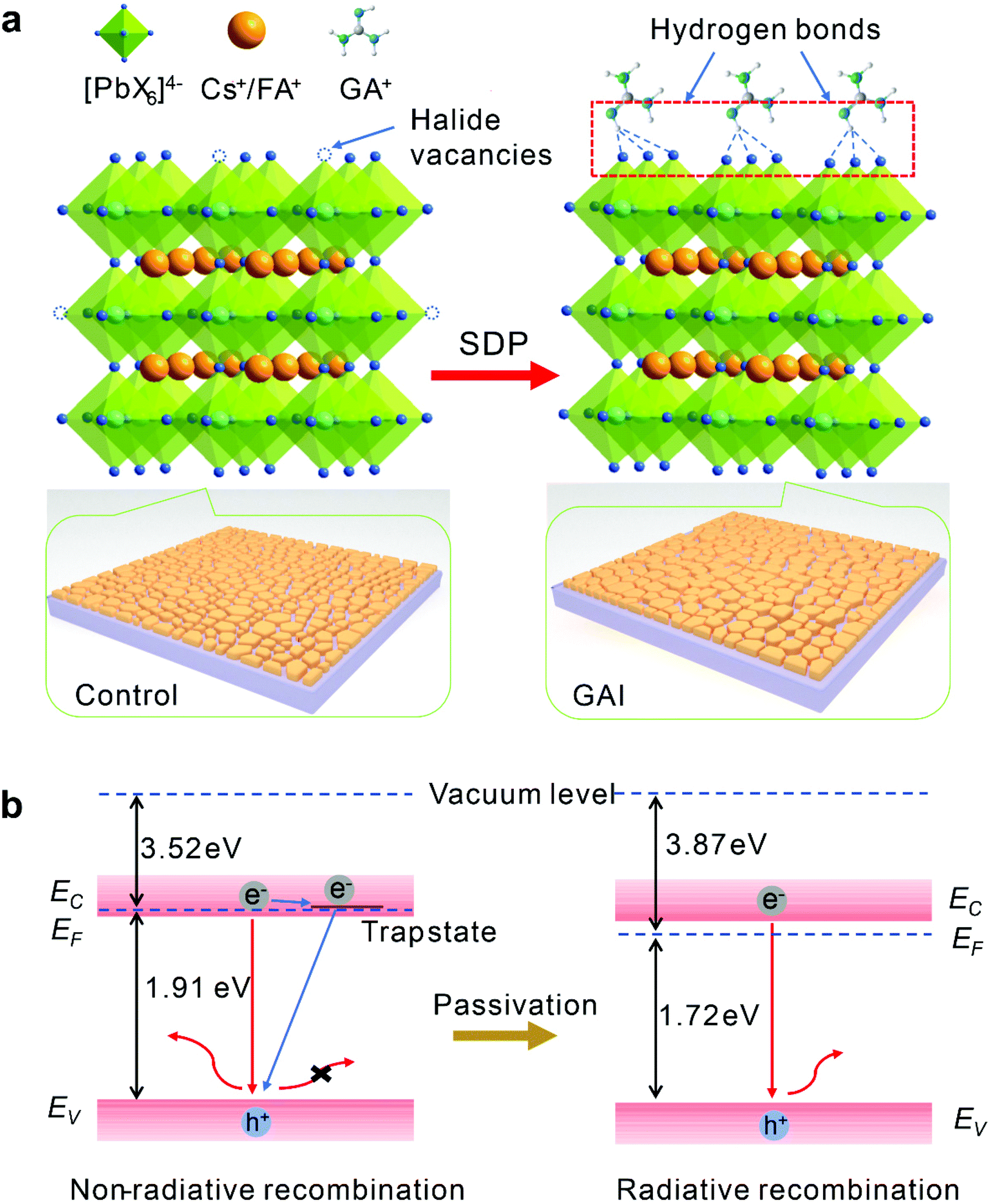 | ||
| Fig. 4 Surface defect passivation (SDP) mechanism of perovskite defects via GAI modification. (a) Schematic illustration and (b) energy level diagrams of defect passivation on the perovskite surface and at the grain boundaries. | ||
Furthermore, ultraviolet photoelectron spectroscopy (UPS) was used to characterize the electronic structures of the perovskite films with GAI modification. According to the secondary electron cutoff region of the perovskite films (Fig. S12†), the work function of the perovskite films was estimated to be increased from 3.52 eV for the control sample to 3.87 eV for the GAI-modified film. At the same time, the valence band edge (Ev) relative to the Fermi level (EF) was reduced from 1.91 eV to 1.72 eV. The energy-level diagrams of these two perovskite films are summarized in Fig. 4b. The EF is pinned to the defect states resulting from the existence of a large number of defects in the control film. After the defects are effectively passivated, the EF will move to its original position.4 Given that the optical bandgap of the perovskite films used here is about 1.8 eV (Fig. 2a), it is reasonable to infer that the EF of the control film will be located near the conduction band edge (Ec). The EF of the GAI-modified perovskite film was downward shifted from the Ec as compared to the case of the control sample. Such an energy level shift can be attributed to the GAI-assisted surface passivation of the halide vacancy-related shallow defect states on the surface and at the grain boundary of the perovskite films. As a result, the trap-mediated non-radiative recombination can be suppressed, and the GAI-modified PeLEDs achieve high luminescence and efficiency.
Finally, the operational stability of the PeLEDs was characterized. Fig. 5a shows the device lifetime measured under a constant current density at an initial luminance of 1000 cd m−2. The half-lifetime (T50) of the GAI-modified PeLED was found to be 563 min, which was longer than that of the control device (102 min). Fig. 5b displays the evolution of the EL spectra of the GAI-modified PeLEDs. It is noteworthy that the device exhibited good operational stability, and the EL spectra remain almost identical for 420 min under a continuous bias of 3 V. According to previous reports,8,39,43 the enhanced device stability can be attributed not only to the suppressed ion migration from defects in the perovskite films, but also to the protected perovskite film from moisture due to the formation of the 2D perovskite capping layer.
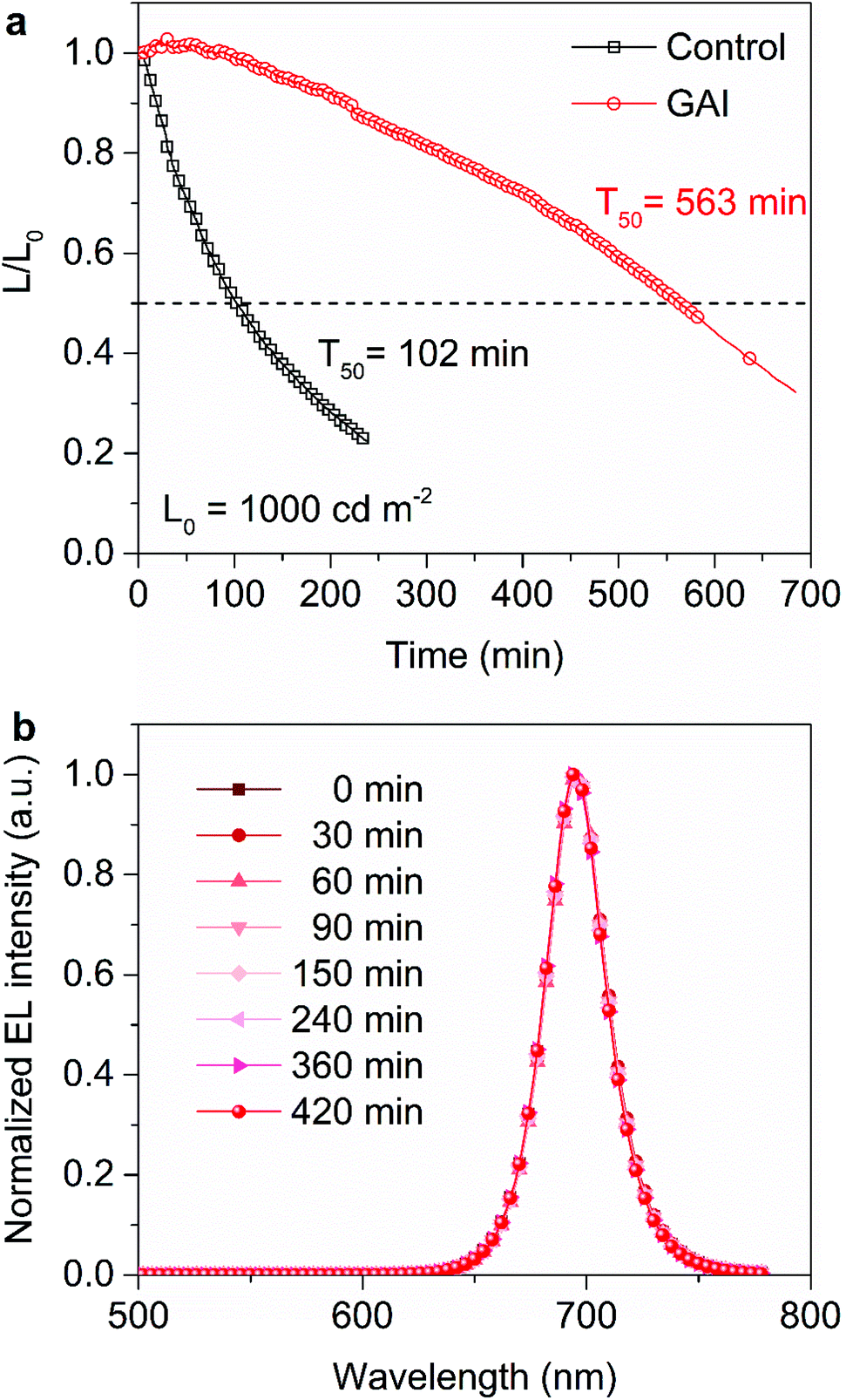 | ||
| Fig. 5 Stability of PeLEDs. (a) Lifetime measurements at an initial luminance of 1000 cd m−2 under a constant current density. (b) EL spectral stability under 3 V continuous applied voltage. | ||
4. Conclusions
In summary, we have demonstrated a surface defect passivation strategy to improve the efficiency and stability of red-emission PeLEDs via the assistance of guanidinium iodide. The GAI modification can enable the secondary grain growth with the formation of surface-2D/bulk-3D heterophased perovskites and the surface defect passivation due to the hydrogen bonding interactions of GA+ ions with halide vacancies. Benefited from the dual effects, the GAI-modified perovskite films are realized with improved optoelectronic properties owing to the reduced trap densities and the suppressed non-radiative recombination. The champion PeLED has achieved an EQE of 17.1% with a pure red-emission at 692 nm. In addition, the devices exhibit good reproducibility with an average EQE of 14.1%, and improved operational stability with a half-lifetime of 563 min at an initial luminance of 1000 cd m−2. This work provides an efficient strategy for defect passivation in perovskite films to achieve high-performance perovskite light-emitting diodes.Author contributions
Yong-Chun Ye synthesized the materials and fabricated the devices; Yu Tian synthesised the ZnO nanoparticles; Xiao-Yi Cai conducted the sample characterization; Yang Shen performed the transient PL measurements; Kong-Chao Shen performed the GIXRD measurements; Yan-Qing Li performed data analysis; Xingyu Gao and Fei Song supported the synchrotron-based characterization; Wenjun Wang contributed important suggestions; Jian-Xin Tang supported this work and revised the manuscript. All authors wrote the manuscript.Conflicts of interest
There are no conflicts to declare.Acknowledgements
The authors acknowledge the beamline BL14B1 at Shanghai Synchrotron Radiation Facility (SSRF) for providing the beam time and the financial support from the National Natural Science Foundation of China (No. 61520106012, 62075061, 61722404, 51873138, 11874380, 11675252, and U1632265), the National Key R&D Program of China (No. 2016YFB0401002 and 2016YFB0400700), the 333 program (No. BRA2019061), and the Collaborative Innovation Center of Suzhou Nano Science & Technology.References
- J.-P. Correa-Baena, M. Saliba, T. Buonassisi, M. Grätzel, A. Abate, W. Tress and A. Hagfeldt, Science, 2017, 358, 739–744 CrossRef CAS PubMed.
- A. Krishna, S. Gottis, M. K. Nazeeruddin and F. Sauvage, Adv. Funct. Mater., 2019, 29, 1806482 CrossRef.
- S. Akin, N. Arora, S. M. Zakeeruddin, M. Grätzel, R. H. Friend and M. I. Dar, Adv. Energy Mater., 2020, 10, 1903090 CrossRef CAS.
- S. Heo, G. Seo, K. T. Cho, Y. Lee, S. Paek, S. Kim, M. Seol, S. H. Kim, D. Yun, K. Kim, J. Park, J. Lee, L. Lechner, T. Rodgers, J. W. Chung, J. Kim, D. Lee, S. Choi and M. K. Nazeeruddin, Adv. Energy Mater., 2019, 9, 1902470 CrossRef CAS.
- D. Luo, W. Yang, Z. Wang, A. Sadhanala, Q. Hu, R. Su, R. Shivanna, G. F. Trindade, J. F. Watts, Z. Xu, T. Liu, K. Chen, F. Ye, P. Wu, L. Zhao, J. Wu, Y. Tu, Y. Zhang, X. Yang, W. Zhang, R. H. Friend, Q. Gong, H. J. Snaith and R. Zhu, Science, 2018, 360, 1442–1446 CrossRef CAS PubMed.
- Q. He, M. Worku, L. Xu, C. Zhou, H. Lin, A. J. Robb, K. Hanson, Y. Xin and B. Ma, ACS Appl. Mater. Interfaces, 2020, 12, 1159–1168 CrossRef CAS PubMed.
- L. N. Quan, B. P. Rand, R. H. Friend, S. G. Mhaisalkar, T.-W. Lee and E. H. Sargent, Chem. Rev., 2019, 119, 7444–7477 CrossRef CAS PubMed.
- S. Lee, D. B. Kim, J. C. Yu, C. H. Jang, J. H. Park, B. R. Lee and M. H. Song, Adv. Mater., 2019, 31, 1805244 CrossRef PubMed.
- T. Han, S. Tan, J. Xue, L. Meng, J. Lee and Y. Yang, Adv. Mater., 2019, 31, 1803515 CrossRef CAS PubMed.
- W. Xu, Q. Hu, S. Bai, C. Bao, Y. Miao, Z. Yuan, T. Borzda, A. J. Barker, E. Tyukalova, Z. Hu, M. Kawecki, H. Wang, Z. Yan, X. Liu, X. Shi, K. Uvdal, M. Fahlman, W. Zhang, M. Duchamp, J.-M. Liu, A. Petrozza, J. Wang, L.-M. Liu, W. Huang and F. Gao, Nat. Photonics, 2019, 13, 418–424 CrossRef CAS.
- K. Lin, J. Xing, L. N. Quan, F. P. G. de Arquer, X. Gong, J. Lu, L. Xie, W. Zhao, D. Zhang, C. Yan, W. Li, X. Liu, Y. Lu, J. Kirman, E. H. Sargent, Q. Xiong and Z. Wei, Nature, 2018, 562, 245–248 CrossRef CAS PubMed.
- Z. Fang, W. Chen, Y. Shi, J. Zhao, S. Chu, J. Zhang and Z. Xiao, Adv. Funct. Mater., 2020, 30, 1909754 CrossRef CAS.
- G. Cheng, Y. Liu, T. Chen, W. Chen, Z. Fang, J. Zhang, L. Ding, X. Li, T. Shi and Z. Xiao, ACS Appl. Mater. Interfaces, 2020, 12, 18084–18090 CrossRef CAS PubMed.
- Z.-K. Tan, R. S. Moghaddam, M. L. Lai, P. Docampo, R. Higler, F. Deschler, M. Price, A. Sadhanala, L. M. Pazos, D. Credgington, F. Hanusch, T. Bein, H. J. Snaith and R. H. Friend, Nat. Nanotechnol., 2014, 9, 687–692 CrossRef CAS PubMed.
- Y. Dong, Y. Zou, J. Song, X. Song and H. Zeng, J. Mater. Chem. C, 2017, 5, 11369–11394 RSC.
- F. P. García de Arquer, A. Armin, P. Meredith and E. H. Sargent, Nat. Rev. Mater., 2017, 2, 16100 CrossRef.
- H. Dong, C. Zhang, X. Liu, J. Yao and Y. S. Zhao, Chem. Soc. Rev., 2020, 49, 951–982 RSC.
- Y. Cao, N. Wang, H. Tian, J. Guo, Y. Wei, H. Chen, Y. Miao, W. Zou, K. Pan, Y. He, H. Cao, Y. Ke, M. Xu, Y. Wang, M. Yang, K. Du, Z. Fu, D. Kong, D. Dai, Y. Jin, G. Li, H. Li, Q. Peng, J. Wang and W. Huang, Nature, 2018, 562, 249–253 CrossRef CAS PubMed.
- H. Cho, S.-H. Jeong, M.-H. Park, Y.-H. Kim, C. Wolf, C.-L. Lee, J. H. Heo, A. Sadhanala, N. Myoung, S. Yoo, S. H. Im, R. H. Friend and T.-W. Lee, Science, 2015, 350, 1222–1225 CrossRef CAS PubMed.
- L.-P. Cheng, J.-S. Huang, Y. Shen, G.-P. Li, X.-K. Liu, W. Li, Y.-H. Wang, Y.-Q. Li, Y. Jiang, F. Gao, C.-S. Lee and J.-X. Tang, Adv. Opt. Mater., 2019, 7, 1801534 CrossRef.
- N. Wang, L. Cheng, R. Ge, S. Zhang, Y. Miao, W. Zou, C. Yi, Y. Sun, Y. Cao, R. Yang, Y. Wei, Q. Guo, Y. Ke, M. Yu, Y. Jin, Y. Liu, Q. Ding, D. Di, L. Yang, G. Xing, H. Tian, C. Jin, F. Gao, R. H. Friend, J. Wang and W. Huang, Nat. Photonics, 2016, 10, 699–704 CrossRef CAS.
- Y. Shen, M.-N. Li, Y. Li, F.-M. Xie, H.-Y. Wu, G.-H. Zhang, L. Chen, S.-T. Lee and J.-X. Tang, ACS Nano, 2020, 14, 6107–6116 CrossRef CAS PubMed.
- X. Yang, X. Zhang, J. Deng, Z. Chu, Q. Jiang, J. Meng, P. Wang, L. Zhang, Z. Yin and J. You, Nat. Commun., 2018, 9, 570 CrossRef PubMed.
- Y. Miao, Y. Ke, N. Wang, W. Zou, M. Xu, Y. Cao, Y. Sun, R. Yang, Y. Wang, Y. Tong, W. Xu, L. Zhang, R. Li, J. Li, H. He, Y. Jin, F. Gao, W. Huang and J. Wang, Nat. Commun., 2019, 10, 3624 CrossRef PubMed.
- Y. Shen, L. Cheng, Y. Li, W. Li, J. Chen, S. Lee and J. Tang, Adv. Mater., 2019, 1901517 CrossRef PubMed.
- S. Lee, J. H. Park, B. R. Lee, E. D. Jung, J. C. Yu, D. Di Nuzzo, R. H. Friend and M. H. Song, J. Phys. Chem. Lett., 2017, 8, 1784–1792 CrossRef CAS PubMed.
- Y. Ke, N. Wang, D. Kong, Y. Cao, Y. He, L. Zhu, Y. Wang, C. Xue, Q. Peng, F. Gao, W. Huang and J. Wang, J. Phys. Chem. Lett., 2019, 10, 380–385 CrossRef PubMed.
- Y. Tian, C. Zhou, M. Worku, X. Wang, Y. Ling, H. Gao, Y. Zhou, Y. Miao, J. Guan and B. Ma, Adv. Mater., 2018, 30, 1707093 CrossRef PubMed.
- T. Zhang, L. Xie, L. Chen, N. Guo, G. Li, Z. Tian, B. Mao and Y. Zhao, Adv. Funct. Mater., 2017, 27, 1603568 CrossRef.
- M.-H. Park, S.-H. Jeong, H.-K. Seo, C. Wolf, Y.-H. Kim, H. Kim, J. Byun, J. S. Kim, H. Cho and T.-W. Lee, Nano Energy, 2017, 42, 157–165 CrossRef CAS.
- M. Yuan, L. N. Quan, R. Comin, G. Walters, R. Sabatini, O. Voznyy, S. Hoogland, Y. Zhao, E. M. Beauregard, P. Kanjanaboos, Z. Lu, D. H. Kim and E. H. Sargent, Nat. Nanotechnol., 2016, 11, 872–877 CrossRef CAS PubMed.
- L. N. Quan, Y. Zhao, F. P. García de Arquer, R. Sabatini, G. Walters, O. Voznyy, R. Comin, Y. Li, J. Z. Fan, H. Tan, J. Pan, M. Yuan, O. M. Bakr, Z. Lu, D. H. Kim and E. H. Sargent, Nano Lett., 2017, 17, 3701–3709 CrossRef CAS PubMed.
- F. Zhang, B. Cai, J. Song, B. Han, B. Zhang and H. Zeng, Adv. Funct. Mater., 2020, 2001732 CrossRef CAS.
- W. Zhang, J. Xiong, J. Li and W. A. Daoud, Sol. RRL, 2020, 4, 2000112 CrossRef CAS.
- W. Zhang, J. Xiong, J. Li and W. A. Daoud, J. Mater. Chem. A, 2019, 7, 9486–9496 RSC.
- O. Nazarenko, M. R. Kotyrba, S. Yakunin, M. Aebli, G. Rainò, B. M. Benin, M. Wörle and M. V. Kovalenko, J. Am. Chem. Soc., 2018, 140, 3850–3853 CrossRef CAS PubMed.
- D. Yang, X. Zhou, R. Yang, Z. Yang, W. Yu, X. Wang, C. Li, S. (Frank) Liu and R. P. H. Chang, Energy Environ. Sci., 2016, 9, 3071–3078 RSC.
- Q. Dong, Y. Fang, Y. Shao, P. Mulligan, J. Qiu, L. Cao and J. Huang, Science, 2015, 347, 967–970 CrossRef CAS PubMed.
- F. Hu, H. Zhang, C. Sun, C. Yin, B. Lv, C. Zhang, W. W. Yu, X. Wang, Y. Zhang and M. Xiao, ACS Nano, 2015, 9, 12410–12416 CrossRef CAS PubMed.
- K. L. Svane, A. C. Forse, C. P. Grey, G. Kieslich, A. K. Cheetham, A. Walsh and K. T. Butler, J. Phys. Chem. Lett., 2017, 8, 6154–6159 CrossRef CAS PubMed.
- C. M. M. Soe, C. C. Stoumpos, M. Kepenekian, B. Traoré, H. Tsai, W. Nie, B. Wang, C. Katan, R. Seshadri, A. D. Mohite, J. Even, T. J. Marks and M. G. Kanatzidis, J. Am. Chem. Soc., 2017, 139, 16297–16309 CrossRef CAS PubMed.
- Q. Zhou, L. Liang, J. Hu, B. Cao, L. Yang, T. Wu, X. Li, B. Zhang and P. Gao, Adv. Energy Mater., 2019, 9, 1802595 CrossRef.
- W. Bi, Q. Cui, P. Jia, X. Huang, Y. Zhong, D. Wu, Y. Tang, S. Shen, Y. Hu, Z. Lou, F. Teng, X. Liu and Y. Hou, ACS Appl. Mater. Interfaces, 2020, 12, 1721–1727 CrossRef CAS PubMed.
Footnote |
| † Electronic supplementary information (ESI) available. See DOI: 10.1039/d0nr07677e |
| This journal is © The Royal Society of Chemistry 2021 |