
A highly sensitive label-free electrochemical immunosensor based on an aligned GaN nanowires array/polydopamine heterointerface modified with Au nanoparticles†
Qingyun
Liu
a,
Taotao
Yang
a,
Yongqin
Ye
b,
Ping
Chen
a,
Xiaoning
Ren
a,
Ai
Rao
a,
Ying
Wan
a,
Bin
Wang
*b and
Zhiqiang
Luo
 *a
*a
aCollege of Life Science and Technology, Huazhong University of Science and Technology, Wuhan 430074, China. E-mail: zhiqiangluo@hust.edu.cn
bDepartment of General Surgery, Shenzhen Children's Hospital, Shenzhen 518026, China. E-mail: szwb1967@126.com
First published on 22nd January 2019
Abstract
Aligned GaN nanowire arrays show great potential not only in optoelectronic devices, but also in sensitive biosensor applications, owing to their excellent chemical stability and biocompatibility, as well as high electron mobility and surface-to-volume ratio. However, to construct electrochemical immunosensors, proper surface modification of GaN nanowires, which can enable efficient charge transfer and provide large densities of immobilization sites for antibodies to anchor, is still challenging. Herein we demonstrate a highly sensitive label-free electrochemical immunosensing platform based on the integration of polydopamine (PDA) on a GaN nanowire surface. The PDA polymer was self-assembled on GaN nanowire surfaces via organic polymerization. The interface dipole layer generated at the GaN nanowire array/PDA polymer heterointerface enabled efficient charge transfer. The aligned GaN nanowire array/PDA hybrids were further modified with gold nanoparticles for subsequent covalent binding of antibodies. The fabricated immunosensor yielded a wide linear range between 0.01 and 100 ng ml−1 and a detection limit as low as 0.003 ng ml−1 for the detection of alpha-fetoprotein (AFP). The immunosensor showed good selectivity, reproducibility, and stability and was utilized in human serum samples for AFP detection. This work demonstrates the superiority of taking advantage of a nanowire array configuration and a semiconductor/polymer heterointerface in an immunosensing platform for sensitivity enhancement.
1. Introduction
Encouraged by the unprecedented progress made in nanoscience and nanotechnology in recent years, nanostructured transducing electrodes have been developed and extensively adopted not only in optoelectronic devices, but also to assist in sensitive and accurate electrochemical immunoassay.1–7 As controlled and systematic assembled 1D nanomaterials, a nanowire array architecture with high alignment exhibits unique advantages of a high surface-to-volume ratio and separate electron transfer paths. These aspects provide considerable advantages to use nanowire arrays as a sensitive electrochemical immunosensor, since the biological interactions occurring at the transducing electrode play an important role in establishing an efficient electrochemical immunosensor.8 For example, nanowire arrays can provide more immobilization sites for targeted antibodies, and the specific immobilization of antibodies on the transducing electrode surfaces improves the capture ability of biomarkers via antibody–antigen recognition, thereby facilitating the transduction of the immunoreaction into electrical signals.8 Therefore, engineered nanoarray structures have been considered as competitive nanostructured electrode candidates for constructing sensitive nanoscale immunosensors.Direct and wide bandgap gallium nitride (GaN), a well-established industrial optoelectronics material, has emerged recently as one of the advanced semiconductor biosensor candidates due to its chemical stability, low toxicity to living cells and high electron mobility.9–14 Most of the reports on GaN electrodes are limited to a thin film configuration; for example, GaN-based planar field effect transistors (FET) have been adopted in detecting DNA probes, pH changes, hydrogen gas and proteins related to cancerous diseases.14–17 Recently, geometry- and position-controlled GaN nanowire arrays have begun to receive significant attention in biosensing utilization, owing to the advantages of a nanowire array configuration coupled with their excellent chemical stability and biocompatibility.18–20 For example, Choi et al. reported a highly sensitive assay for cancer antigen CA15-3 detection by employing (3-aminopropyl) triethoxy silane functionalized GaN nanowires as sensing platforms, which allow detection of an individual fluorescence signal under a relatively low background signal.18 Additionally, our previous studies have also demonstrated the feasibility of bare and functionalized GaN nanowires in silver ion detection.20
Since nanomaterials have charge carriers limited or close to the electrode/electrolyte interface, the presence of an antibody–antigen complex may significantly affect the accumulation or depletion of interfacial charge carriers, thus generating a remarkable readout signal change.21 The sensitivity of the GaN nanowires could be further strengthened by modulating the electrode surface with appropriate tethered organic molecules. Inspired by a mussel-adhesion phenomenon, biofunctionalized GaN nanowire arrays can be manufactured gently through direct encapsulation using polydopamine (PDA). Actually, surface modifications of nanomaterials with PDA have gained increasing interest.22–24 The as-formed adherent PDA coating has a surface occupied by abundant active catechol and amine groups, capable of serving as reductants, binding reagents and universal platforms for secondary reactions.22 However, in most of the cases, the assembly of the sensing electrodes is confined to coupling PDA with metals (Au) or narrow bandgap semiconductors (carbon nanotubes). For example, PDA-modified Au nanotubes have been reported to be utilized as a sensitive alpha-fetoprotein (AFP) electrochemical immunosensor.25 A similar result has also been reported on a PDA-coated carbon nanotube–Prussian blue-modified glassy carbon electrode.26 Semiconductors with wide bandgaps have the potential to make a good match with the typical HOMO–LUMO gaps of PDA biomolecules.19,27 Therefore, it is expected that integration of PDA on the GaN nanowire surface will enhance the electrode conductivity by taking full advantage of the semiconductor/organic heterointerface.
Herein, a versatile protocol to utilize a GaN nanowire array/PDA heterointerface as the sensitive transducing matrix in an electrochemical immunosensor has been demonstrated. The strategy employed here was based on the combined advantages contributed by both vertically-grown GaN nanowires and those functionalized with the PDA polymer. The PDA-modified GaN nanowire array was further treated with gold nanoparticles (Au NPs) to obtain an increasing antibody (Ab1) immobilization amount. As a demonstration of the capability of our protocol, AFP was chosen as a model biomarker for our electrochemical immunosensor. AFP, an oncogenic glycoprotein, is one of the most extensively used cancer biomarkers.28 Accurate early detection of AFP is of great importance for proper prevention, diagnosis and treatment of cancers, since an increasing level of AFP in the human body is related to tumor cell growth and thus it has been demonstrated to be a clinical indication for several cancerous diseases such as hepatocellular, yolk sac and testicular cancer.29 Various immunoassay methods have been reported for AFP detection, including chemiluminescence,30 fluorescence,31 and surface plasmon resonance.32 For instance, Zhang's group constructed an ultrasensitive photoelectrochemical biosensor by coupling a highly conductive graphite flake, graphene oxide and alkylated C60 to a metal-free all-carbon nanohybrid to achieve an ultralow AFP detection limit.33 The electrochemical bioassay for AFP detection has also gained great research interest due to its high sensitivity, low cost, ease of portability and simple instrumentation.34–37 Using our as-developed electrochemical immunosensor based on a GaN nanowire array/PDA heterointerface modified with Au NPs, the label-free detection of AFP was achieved in a wide linear range of 0.01–100 ng ml−1 and with a detection limit as low as 0.003 ng ml−1. The present work demonstrated the feasibility of the GaN nanoarray structures for application in biological immunosensing.
2. Experimental
2.1 Reagents and materials
P-type GaN substrates were purchased from Nanowingen Nanotechnology Company (Suzhou, China). Dopamine hydrochloride, (3-aminopropyl)triethoxysilane (APTES) and chloroauric acid (HAuCl4·3H2O) were purchased from Sigma-Aldrich (USA). Gallium oxide (Ga2O3), sodium citrate, potassium ferricyanide (K3Fe(CN)6) and potassium ferrocyanide (K4Fe(CN)6·3H2O) were purchased from Sinopharm Chemical Reagent Co., Ltd (Shanghai, China). Alpha-fetoprotein antigen (AFP), alpha-fetoprotein monoclonal antibody (anti-AFP) and carcinoembryonic antigen (CEA) were purchased from Biocell Biotechnology Co., Ltd (Zhengzhou, China). Bovine serum albumin (BSA), prostate specific antigens (PSA), cancer antigen 125 (CA 125), and human immunoglobulin G (HIgG) were purchased from Bosaitu Biotechnology Company (Zhengzhou, China). Human serum was purchased from Hongquan bio-tel (Guangzhou, China) and was diluted with deionized water (1![[thin space (1/6-em)]](https://www.rsc.org/images/entities/char_2009.gif) :99) before utilization. Phosphate buffered saline (PBS, pH = 7.4) was prepared by mixing 0.1 M sodium dihydrogen phosphate (NaH2PO4·2H2O) and 0.1 M disodium hydrogen phosphate (Na2HPO4·12H2O) (v:v = 81:19) stock solutions. All other reagents were of analytical grade and used without further purification. Ultrapure water from a Milli-Q system (Millipore Direct-Q 5UV) with a resistivity of 18.2 Ω cm was used in all experimental runs.
:99) before utilization. Phosphate buffered saline (PBS, pH = 7.4) was prepared by mixing 0.1 M sodium dihydrogen phosphate (NaH2PO4·2H2O) and 0.1 M disodium hydrogen phosphate (Na2HPO4·12H2O) (v:v = 81:19) stock solutions. All other reagents were of analytical grade and used without further purification. Ultrapure water from a Milli-Q system (Millipore Direct-Q 5UV) with a resistivity of 18.2 Ω cm was used in all experimental runs.
2.2 Apparatus
The synthesis of GaN nanowire arrays was performed in a homemade tubular furnace. The morphology and composition purity were characterized using a field-emission scanning electron microscope operating at 20 kV (FESEM, HITACHI, SU8000) attached to a Dektak XT stylus profiler. The structure was characterized using an X-ray diffraction spectrometer (XRD, SmartLab-SE) with Cu Kα radiation, operating at 40 kV and 40 mA. The morphology and composition distribution of individual nanowires were observed using a transmission electron microscope operating at 200 kV (TEM, FEI, Tecnai G2 F20) attached to an X-ray energy dispersive spectrometer (EDS). Absorption spectra were obtained using a UV-vis-NIR diffuse reflectance spectrometer (DRS, Shimadzu Corporation UV-3600) for band gap calculations. The energy levels were measured by ultraviolet photoelectron spectroscopy (UPS, Thermo ESCALAB 250XI) by using a He I source (21.22 eV). Electrochemical measurements were carried out on a Chenhua CHI660E electrochemical workstation (Shanghai, China).2.3 Synthesis of GaN nanowire arrays
GaN nanowire arrays were prepared through a simple chemical vapor deposition (CVD) process, as described in our previous work.38 Briefly, an α-Al2O3 substrate coated with a 4.5 μm GaN layer by hydrogen vapor phase deposition (HVPE) was commercially produced. Before growth, a 5 nm gold layer was deposited on GaN substrates as a catalyst. An alumina boat filled with Ga2O3 powder was placed in the center of a quartz tube in a tubular furnace. The temperature was increased to 1100 °C from room temperature under high purity gaseous ammonia protection (NH3, 10 sccm) and it was kept for 30 min. After reaction, the furnace was cooled down to room temperature under the protection of gaseous argon (Ar, 100 sccm). Similarly, randomly-assembled GaN nanowires (referred to as GaN nanowires thereinafter) were prepared under identical conditions, except for tuning the NH3 flowing rate from 10 sccm to 100 sccm.2.4 Preparation of GaN-based electrodes
GaN nanowires were immersed in 20 ml piranha solution (H2SO4:H2O2 = 3:1 v/v) and hydrochloric acid (HCl:H2O = 1:1 v/v) for 20 min, respectively, for surface hydroxylation as well as cleaning. The samples were further coated with polydopamine (PDA) via a simple dip-coating method.22 First, 0.06057 g tri(hydroxymethyl)aminomethane (Tris) was dissolved in 25 ml deionised water to obtain 20 mM Tris solution. The pH of the Tris solution was adjusted using 20 mM HCl solution to reach pH = 8.5 and then diluted with deionised water to make 50 ml. Second, the as-synthesized GaN nanowire array samples were dipped and suspended in 50 ml 10 mM Tris–HCl (pH = 8.5). The samples were kept vertical to prevent non-specific microparticle deposition. Third, 0.01 g dopamine hydrochloride was added into the Tris–HCl buffer solution under gentle stirring for a certain number of hours. The mixed solution turned dark brown and finally dark grey during the pH-induced oxidation reaction. The samples coated with PDA were gently rinsed with deionized water several times and dried with N2 gas. The as-obtained samples were stored at 4 °C for later use.
2.5 Synthesis of Au NPs-decorated PDA-coated GaN nanowire arrays
At first, uniform gold colloids with a diameter of ca.13 nm were prepared by rapid injection of 5 ml 38.8 nM sodium citrate into 50 ml 1 mM HAuCl4 boiling solution under vigorous stirring.39 After boiling for 15 min, the solution was cooled down to room temperature and stored at 4 °C for later use. The as-obtained dark red solution was characterized and is shown in Fig. S1 (ESI†). The PDA-coated GaN nanowire array samples were immersed in 3 ml gold colloidal solution and placed in a constant temperature oscillator (37 °C, 200R) overnight. Later, the samples were rinsed with deionized water and dried using N2 gas.GaN thin film/PDA/Au NPs and GaN nanowires/PDA/Au NPs were prepared through an identical procedure. The GaN nanowire array decorated with Au NPs was treated with a slight difference. GaN nanowires were first treated in piranha solution at 80 °C for 50 min. After rinsing with deionised water, they were immersed in 1% (v/v) 3-APTES in ethanol at room temperature for 1 h under constant shaking (25 °C, 100 R). Then they were rinsed with ethanol and placed on a hot plate at 120 °C for 10 min, respectively. The Au NPs deposition process was the same as mentioned above.
2.6 Construction of the immunosensor
The general strategy for the immunosensor construction is displayed in Scheme 1. Firstly, the GaN nanowire array/PDA/Au NPs electrodes were immersed in 9.323 μg ml−1 anti-AFP antibody solution and incubated at 37 °C. Then they were gently washed with 0.1 M PBS (pH = 7.4) to exclude any physically adsorbed antibodies. Secondly, to avoid non-specific adsorption, the modified electrodes were immersed in 1 mg ml−1 BSA solution for extra site blocking and rinsed with PBS. Lastly, the modified electrodes were immersed in an AFP antigen solution of a specific concentration and incubated at 37 °C. After gentle washing in PBS, the immunosensors used for electrochemical characterization were obtained.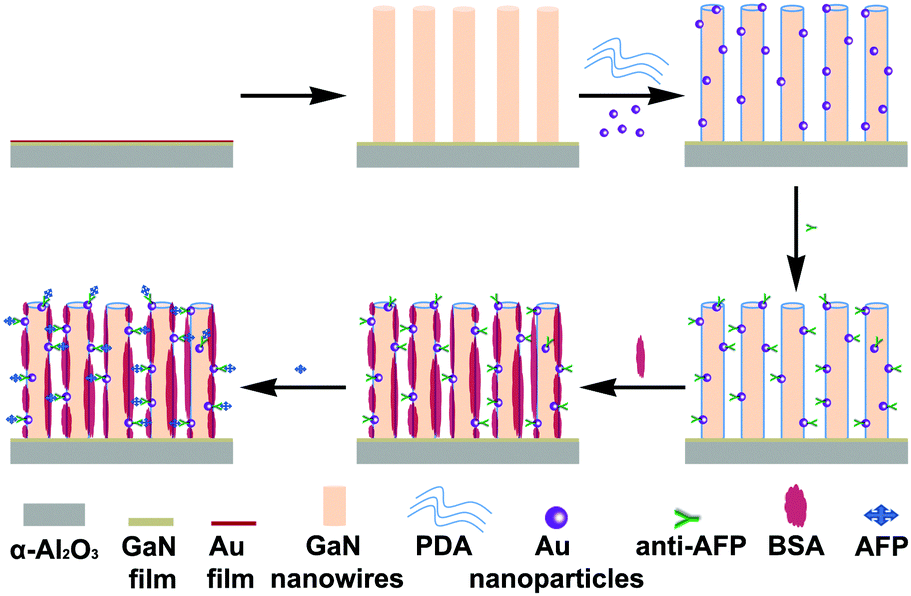 | ||
| Scheme 1 General strategy for the fabrication process of the GaN nanowire array/PDA/Au NPs immunosensor. | ||
2.7 Electrochemical characterization
All electrochemical measurements were carried out on an electrochemical workstation at room temperature. A standard three-electrode configuration was adopted for the electrolytic system, including GaN as the working electrode, a platinum tablet (5 mm × 5 mm) as the counter electrode and Ag/AgCl (3 M KCl) as the reference electrode. The working electrodes were fixed with an electrode holder and immersed in an electrolyte solution containing 5 mM K3Fe(CN)6/K4Fe(CN)6 (1:1) and 0.1 M KCl, where [Fe(CN)6]4−/3− acted as a redox probe. Cyclic voltammetry (CV) and electrochemical impedance spectroscopy (EIS) were adopted in each electrode modification and immunosensor fabrication process. Differential pulse voltammetry (DPV) was adopted in the calibration process. CV spectra were recorded at an applied potential from −0.6 V to 1.0 V (vs. Ag/AgCl) at a scan rate of 100 mV s−1. EIS spectra were recorded in a frequency range of 0.1 Hz to 10000 Hz, with an amplitude of 5 mV. DPV measurements were obtained at an applied potential from −0.2 V to 0.6 V (vs. Ag/AgCl).
3. Results and discussion
3.1 Characterization of GaN nanowire array polydopamine/gold nanoparticles composite
Fig. 1a–c show plan view, 40°-tilted and cross-sectional scanning electron microscopy (SEM) images of a GaN nanowire array prepared by a simple CVD method. A large number of nanowires was observed to grow on a heavily-doped p-type GaN substrate with uniform alignment. From the low magnification SEM image in Fig. 1c, it can be seen that highly-aligned GaN nanowires were epitaxially grown on the GaN buffer layer (with a thickness of ca. 4.5 μm). The inset magnified SEM images revealed that the GaN nanowires were ca. 200 nm in diameter, up to 10 μm in length, and possessed a hexagonal cross section with catalytic gold nanoparticles (Au NPs) on the tips. Contrary to commonly observed smooth side facets, the vertically-aligned GaN nanowires exhibited a periodic corrugated morphology, as shown in the inset in Fig. 1a and b. It is assumed that the periodic concave and convex crystalline planes are due to the oscillation in nanowires’ radial growth, combined with electrostatic interaction energy equilibrium.38 Structural analysis with XRD proved the vertically-grown nanowires to be a wurtzite GaN single crystal with high alignment along [001], by showing a predominant and singular diffraction peak at 34.55° indexed to the (002) planes (Fig. 1d). Quantitative composition analysis on the GaN nanowires also confirmed the high purity of the GaN nanowires by showing exclusive N and Ga elements (Fig. 1e). Elemental mapping of a randomly selected area revealed the uniform distribution of Ga and N elements (Fig. 1f).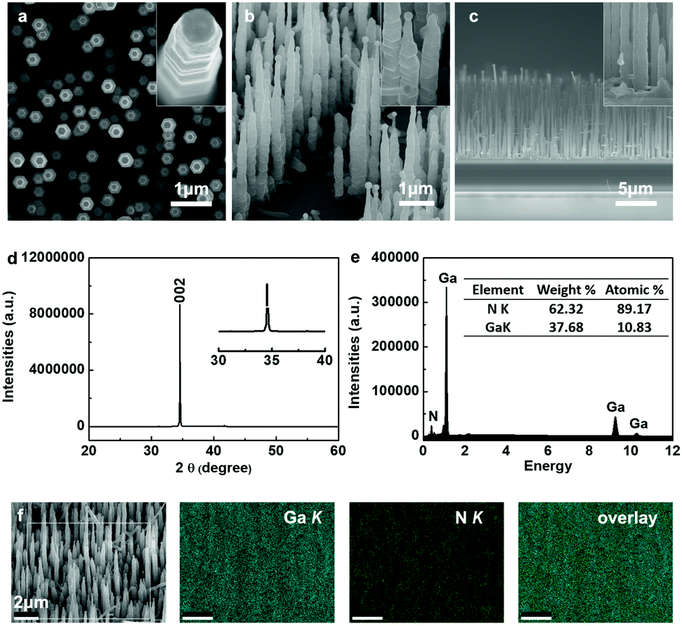 | ||
| Fig. 1 (a–c) Low magnification plan view, 40°-tilted and cross-sectional SEM images of a highly-aligned GaN nanowire array (from left to right), a GaN layer with a thickness of 4.5 μm can be observed in (c); insets show the magnified SEM images for an individual nanowire. (d) XRD pattern of highly-aligned GaN nanowire array, a predominant peak is observed at 34.55°, indexed to the (002) plane in the wurtzite GaN crystal; inset in (d) shows the diffraction peak at 34.55°. (e) EDS spectrum shows distinctive Ga and N peaks and (f) the corresponding EDS elemental mapping shows exclusive Ga and N elements. In (f) from left to right represents the SEM, Ga K, N K, and overlay image, respectively. | ||
The GaN nanowire array was dipped in Tris–HCl buffer solution by dissolving 0.01 g dopamine hydrochloride for polydopamine (PDA) coating. After coating with PDA, the substrate slice displayed a light grey color, while the substrate with bare GaN nanowires usually appeared light yellow. Then it was immersed in a nanogold colloidal solution to allow gold nanoparticles (Au NPs) adsorption onto the nanowire surfaces. Meanwhile, the substrate turned dark red, indicating the successful deposition of the Au NPs. Fig. 2a–c show the representative SEM images of GaN nanowire arrays in stepwise modification processes. After PDA coating, the nanowire surfaces became smoother (Fig. 2b) compared with those of bare GaN nanowires, where the latter had periodic corrugated side facets (Fig. 2a). In Fig. 2c, the Au NPs were observed to distribute uniformly on the surfaces of the GaN nanowire array/PDA hybrid.
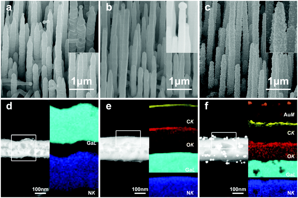 | ||
| Fig. 2 Representative 40°-tilted SEM images for (a) GaN nanowire array, (b) GaN nanowire array/PDA and (c) GaN nanowire array/PDA/Au NPs; insets display the morphology of individual nanowires after each assembly step. STEM images for an individual nanowire after each step and its corresponding spatially resolved elemental mapping are shown in (d–f), respectively. The selected areas for compositional analysis are marked by white squares at the left side. | ||
Scanning transmission electron microscopy (STEM) was adopted to observe the morphology and characterize the compositional distribution of individual nanowires at the atomic scale. Before modification, bare crystalline GaN nanowires showed two elements, Ga element and N element, consistent with the quantitative composition analysis performed in SEM characterization (Fig. 2d). Two additional signals, C and O elements, were collected from the GaN nanowire coated with PDA, providing another piece of evidence for the existence of PDA (Fig. 2e). It is worth noting that both C and O signals were strong at the top but became weaker along the radial direction. This is possibly because comparatively stronger Ga and N signals originated from the GaN nanowires. Similarly, GaN nanowire/PDA hybrid/Au NPs exhibited distinctive Au signals apart from Ga, N, C and O signals (Fig. 2f). Consistent results can also be observed in transmission electron microscopy (TEM) images (Fig. S2a–c, ESI†). The high-resolution TEM image in Fig. S2d (ESI†) revealed succinct diffraction spots of a single crystalline Au NP and GaN nanowire, as well as PDA coating on the nanowire surface.
3.2 Optimization of the modified GaN nanowire array
The electrochemical performance of the stepwise modified GaN nanowire array was monitored by cyclic voltammetry (CV) and electrochemical impedance spectroscopy (EIS) measurements. Fig. 3 shows the CV and EIS curves of the modified GaN nanowire array electrodes characterized in 0.5 mM [Fe(CN)6]3−/4− and 0.1 M KCl electrolyte after each assembly step. In Fig. 3a, the CV plot of the bare GaN nanowire arrays showed significant oxidation and reduction peaks at a scanning rate of 100 mV s−1 in the range from −0.6 V (vs. Ag/AgCl) to 1 V (vs. Ag/AgCl), suggesting highly reversible electrochemical reactions at the electrode surface. Coating of a PDA layer on the GaN nanowires made the peak current increase over the voltage range, indicating that the charge transfer between the GaN nanowires and PDA linker was promoted. Thereafter, Au NPs deposition gave a further increase in the current signal, which could be attributed to the good conductivity of nanogold. Subsequently, impedance measurements were adopted to analyze the detailed information on electrical resistance and capacitance changes at the heterointerface. EIS results are shown in Fig. 3b by Nyquist plots, imaginary impedance Z′′(ω) vs. real impedance Z′(ω), of a stepwise modified GaN nanowire array electrode. The Z′(ω) and Z′′(ω) are adjusted to the same scale in order to show the angle of the inclined line at the low frequency region.40 The impedance spectrum included a 30° inclined line at the low frequency region (a diffusion limited process) and a semicircle at the higher frequency region (a electron transfer dominated process). As the modification process proceeded, the semicircles in the higher frequency region decreased in the sequence of GaN nanowire array, GaN nanowire array/PDA and GaN nanowire array/PDA/Au NPs. The semicircle diameter equals the electron transfer resistance Ret. From the fitted parameters shown in Table S1 (ESI†), it can be inferred that the Ret values were decreased significantly from 448.2 Ω (GaN nanowire array) to 188.2 Ω (GaN nanowire array/PDA) and 96.04 Ω (GaN nanowire array/PDA/Au NPs). Thus, the smaller semicircle diameter indicated the smaller electron transfer resistance, in other words, the electron transfer step became faster at the surface of the modified electrode,41 which is consistent with the results of the CV measurement.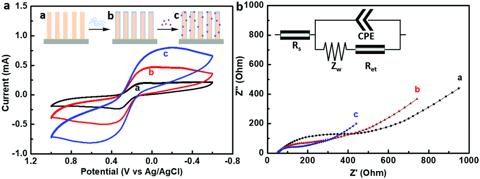 | ||
| Fig. 3 (a) Variation of cyclic voltammograms and (b) electrochemical impedance spectra with the modified GaN nanowire array at a scan rate of 100 mV s−1: (a) bare GaN nanowire array, (b) GaN nanowire array/PDA, (c) GaN nanowire array/PDA/Au NPs; the corresponding schematic diagram is shown at the top in (a) to describe the modification process; an electronic equivalent circuit shown at the top in (b) is used to model the interfacial phenomenon, where Rs represents the ohmic resistance of the [Fe(CN)6]3−/4− electrolyte, Zw represents Warburg impedance, Ret is the electron transfer resistance and CPE represents the capacitance of the GaN nanowire array electrode with a rough surface. | ||
Generally, the Ret value of PDA is associated with polymerization time.42 The relationship of the current increment (ΔI) with the PDA polymerization time was characterized by CV and shown in Fig. S3a (ESI†). It can be inferred that the current increased significantly with the PDA polymerization time from 1 h to 5 h. This might be attributed to the decreased Ret value at the GaN/PDA heterointerface. However, the current change was not obvious when the polymerization time extended from 5 h to 20 h. Therefore, 5 h was chosen as the optimal polymerization time. From the HRTEM images (Fig. S2d, ESI†) it can be estimated that the thickness of the PDA layer reached 5 nm after 5 h. The Au NPs densities were also investigated by dipping the electrodes in the colloidal Au solution for different times. The current reached the maximum after 12 h deposition and remained unchanged since then. Thus, the Au NPs deposition time was chosen to be 12 h (Fig. S3b, ESI†).
To this end, direct bandgap GaN nanowires appear to be a suitable candidate semiconductor to make electronic contact with PDA due to its wide bandgap (3.4 eV)38 and few defects at the interface (Fig. S2d, ESI†). It is believed that the heterointerfaces between the semiconductors and the biomolecules are beneficial for electrochemistry applications. In an ideal situation, the biomolecules are covalently immobilized on the semiconductor surface via a proper mediate, namely linker molecules. The influence of an interface dipole (IDP) layer and of interface defects is necessary to consider, as depicted in Fig. S4a (ESI†). In order to promote the electronic properties, the defects at the interface with area densities below 1011 to 1012 have to be ensured.27 On the other hand, the potential energy jump caused by the IDP layer can have a significant effect on the overall electronic properties. The band offset occurring at the IDP layer is closely related to the position of the molecular electronic levels in the linker molecules, i.e. the highest occupied molecular orbital (HOMO) and the lowest unoccupied molecular orbital (LUMO). From the energy levels of GaN and PDA shown in Fig. S4a (ESI†), which are determined by ultraviolet photoelectron spectroscopy (UPS, Fig. S4b and c, ESI†) and UV-vis diffuse reflectance spectroscopy (DRS, Fig. S4d–f, ESI†), it has been suggested that efficient charge transfer between the wide bandgap semiconductors and the linker molecules is possible due to the relatively small electronic barriers.47
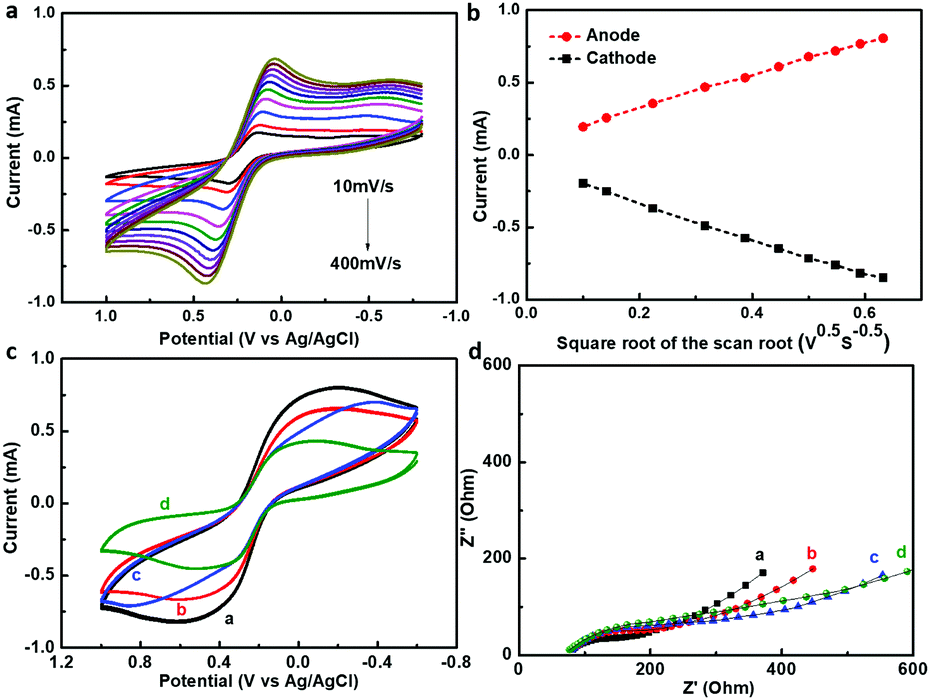 | ||
| Fig. 4 (a) Cyclic voltammograms of the bare GaN nanowire array at different scan rates (10 mV s−1, 20 mV s−1, 50 mV s−1, 100 mV s−1, 150 mV s−1, 200 mV s−1, 250 mV s−1, 300 mV s−1, 350 mV s−1, and 400 mV s−1); (b) corresponding cathodic (black) and anodic (red) peak currents versus square root of scan rates from 10 mV s−1 to 400 mV s−1 in (a); (c) cyclic voltammograms and (d) electrochemical impedance spectra of the electrode after each step of the fabrication process: (a) GaN nanowire array/PDA/Au NPs, (b) GaN nanowire array/PDA/Au NPs/Ab1, (c) GaN nanowire array/PDA/Au NPs/Ab1/BSA, (d) GaN nanowire array/PDA/Au NPs/Ab1/BSA/AFP. | ||
The morphologies of the GaN electrodes were manipulated to investigate the structure–electronic property relationship. Fig. S5a–c (ESI†) shows the SEM images of the modified GaN electrodes with diverse morphologies. The corresponding Nyquist plot is shown in Fig. S5e (ESI†). It can be clearly seen that the GaN nanowire array/PDA/Au NPs electrode exhibited the smallest semicircle diameter, GaN nanowire/PDA/Au NPs were larger and GaN film/PDA/Au NPs were the largest; the Ret value was in the following order: GaN nanowire array/PDA/Au NPs < GaN nanowires/PDA/Au NPs < GaN film/PDA/Au NPs. The influence of the PDA coating on the Ret value was also investigated. The semicircle diameter of the GaN nanowire array/Au NPs was larger than that of both the GaN nanowire array and GaN nanowires modified with PDA and Au NPs, but smaller than that of GaN film/PDA/Au NPs (Fig. S5e, ESI†). These results illustrated that the conductivity of the GaN nanowires with high alignment is superior to that of either randomly-assembled or planar counterparts, which might be attributed to the high electron mobility of the GaN nanowires assembled onto the conductive layer while the conductive layer acted as a transport channel.20 In addition, the PDA/Au NPs modified GaN nanowires exhibited better conductivity than the GaN nanowires covalently functionalized with Au NPs, which might be ascribed to the GaN/PDA heterointerface.47
3.3 Construction of GaN nanowire array based immunosensors
The electrochemical properties of the modified GaN nanowire array electrode were characterized before immunosensor fabrication. Fig. 4a shows the relationship between the scanning rates and peak currents in the modified GaN nanowire array/PDA/Au NPs electrode. Well-defined redox waves were observed at scanning rates from 10 mV s−1 to 400 mV s−1, with ΔEp and IPox/IPred of 165 mV and 0.989 at a scanning rate of 10 mV s−1. The corresponding anodic and cathodic peak currents showed a linear dependence on the square root of the scanning rate (Fig. 4b). It can be deduced that the electrochemical reaction on the GaN nanowire surface is mass-transfer controlled.The step-by-step fabrication process and the electrochemical performances of the immunosensor were monitored by CV and EIS measurements. As shown in Fig. 4c, the CV plot of the GaN nanowire array/PDA/Au NPs exhibited two well-defined reduction and oxidation peaks. After continuous loading of Ab1, BSA and AFP on the electrode surface, the current responses decreased gradually, which were caused by inhibited interfacial electron transfer. This could be easily understood since the insulating immobilized proteins usually exhibit poor conductivity which is expected to retard the charge transfer kinetics at the electrode surface. The electrochemical impedance during the immunosensor fabrication process was also presented by a Nyquist plot in Fig. 4d. It can be observed that the diameters of the semicircles on the Nyquist plots increased with the successive assembly of Ab1, BSA and AFP on the electrode surface, which indicated that the interfacial electron transfer resistance grew larger. The consistent results in the CV and EIS spectrum confirmed the successful construction of the GaN nanowire array/PDA/Au NPs immunosensor.
Prior to the detection of AFP, the detection conditions were optimized for better analytical performance. The incubation time for the anti-AFP antibody and AFP antigen is an important factor, and thus has been carefully examined. Fig. S6a (ESI†) shows a rapid inhibition ratio increase of the current response from 60 min to 120 min, but afterwards a slight change was observed from 60 min to 180 min. This could be due to the saturated number of antibodies binding on the electrode surface after 120 min. Therefore, 120 min was chosen as the incubation time for the anti-AFP antibody. The influence of the AFP incubation time was investigated using 1 ng ml−1 AFP. Fig. S6b (ESI†) shows that the current response inhibition ratio increased with the incubation time and reached the maximum after 120 min, indicating the saturated AFP antigens on anti-AFP antibodies after 120 min. Thus, 120 min was chosen as the incubation time for AFP antigens.
Under optimal conditions, the sensitivity and dynamic range of the as-prepared immunosensor was evaluated by differential pulse voltammetry (DPV). The fabricated immunosensor was adopted for antigen detection with different AFP concentrations from 0.01 ng ml−1 to 100 ng ml−1. Fig. 5a shows that the DPV peak currents decreased with the incremental AFP concentrations in the detecting range. The corresponding calibration plots displayed a good linear relationship between the peak current inhibition ratio and the examined AFP antigen concentrations with a correlation coefficient of R2 = 0.989 (Fig. 5b). The linear relationship was established to be
| y = 0.421 + 0.104lg[CAFP (ng ml−1)] | (1) |
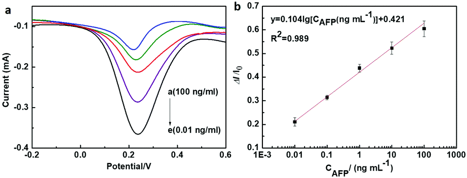 | ||
| Fig. 5 (a) Differential pulse voltammetry of the as-prepared immunosensors in the presence of AFP with different concentrations (0.01 ng ml−1, 0.1 ng ml−1, 1 ng ml−1, 10 ng ml−1, and 100 ng ml−1). (b) Corresponding calibration curve for AFP detection, the error bars represent the standard deviation obtained from three measurements (n = 3). | ||
| Immunosensors | Linear range (ng ml−1) | Detection limit (ng ml−1) | Ref. |
|---|---|---|---|
| ITO/TiO2/CdS | 5 × 10⁻²–5 × 10 | 4 × 10⁻² | 43 |
| Ag wire-graphene | 5 × 10⁻²–4 × 10² | 5 × 10⁻³ | 44 |
| MWCNTs/SiO2 nanoparticle array | 1 × 10⁻¹–3 × 10 | 2 × 10⁻² | 45 |
| PDA/ZnO nanorods | 1 × 10⁻¹–5 × 10² | 1 × 10⁻² | 46 |
| Au NPs/PDA/GaN nanowire array | 1 × 10⁻²–1 × 10² | 3 × 10⁻³ | This work |
The selectivity, repeatability and stability of the immunosensor are important factors for biological applications. Firstly, the selectivity was investigated by adding several potential interferences, including carcinoembryonic antigen (CEA), bovine serum albumin (BSA), prostate specific antigens (PSAs), human immunoglobulin G (IgG) and cancer antigen 125 (CA 125), to the immunosensor separately (Fig. S7a, ESI†). The inhibition ratios of the interference biomolecules were less than 5% except for CA 125, which was also less than 8%. Compared with the inhibition ratio obtained from 0.1 ng ml−1 AFP antigen, the variation caused by the high concentration interference substances was negligible. The stability was investigated by checking the current responses periodically (Fig. S7c, ESI†). The immunosensor exhibited an initial inhibition ratio of 43.82%. After 7 days and 15 days of restoring at 4 °C, it retained 40.79% and 39.44%, respectively, which demonstrated that the immunosensor was stable. Lastly, the repeatability was examined by detecting five independent immunosensors constructed with 1 ng ml−1 AFP antigen under identical conditions. The relative standard deviation (RSD) was 4.98%, suggesting that the repeatability was acceptable (Fig. S7b, ESI†). These results confirmed the excellent selectivity, repeatability and stability of the immunosensor for AFP detection. To evaluate the practicability of the immunosensor in real sample detection, a series of amounts of AFP were added into diluted human serum and the detection results are displayed in Table S2 (ESI†). The recovery was between 98.42% and 105.70% and the RSD was below 5%, which indicated that the immunosensor possessed a relatively good accuracy in real sample detection. The concentration range of AFP in human serum for several common neoplasms is listed in Table S3 (ESI†), and it can be seen that the immunosensor has potential for practical applications.
4. Conclusions
In summary, PDA/Au NPs modified highly-aligned GaN nanowire arrays have been proved to be a competitive candidate in realizing ultrasensitive label-free electrochemical immunosensors. By taking advantage of the nanoarray geometry and the IDP layer formed at the heterointerface of wide bandgap semiconductor GaN/organic PDA polymer, the working electrode showed reduced electron transfer resistance by showing a low detection limit down to 0.003 ng ml−1. Comparative studies on the surface resistance conducted on randomly-assembled nanowires and film counterparts revealed the excellent conductivity of the GaN nanowire array/PDA/Au NPs immunosensor. Furthermore, the immunosensor yielded satisfactory selectivity, stability, and reproducibility and exhibited acceptable quantitative determination of AFP in human serum samples. The GaN nanowire array emerges as a potential candidate in biosensing and could be utilized as an effective electrode for detection of other biomolecules.Conflicts of interest
The authors declare no conflicts of interest.Acknowledgements
This work was supported by the China Postdoctoral Science Foundation project (grant number 2017M622431), and Zhiqiang Luo and Bin Wang acknowledge the support from the Sanming Project of Medicine in Shenzhen (grant number SZSM201812055).References
- T. Cossuet, J. Resende, L. Rapenne, O. Chaix-Pluchery, C. Jimenez, G. Renou, A. J. Pearson, R. L. Z. Hoye, D. Blanc-Pelissier, N. D. Nguyen, E. Appert, D. Munoz-Rojas, V. Consonni and J. L. Deschanvres, Adv. Funct. Mater., 2018, 28, 12 CrossRef.
- S. Lu, Q. Liao, J. Qi, S. Liu, Y. Liu, Q. Liang, G. Zhang and Y. Zhang, Nano Res., 2016, 9, 372–379 CrossRef CAS.
- C. Xie, B. Nie, L. H. Zeng, F. X. Liang, M. Z. Wang, L. B. Luo, M. Feng, Y. Q. Yu, C. Y. Wu, Y. C. Wu and S. H. Yu, ACS Nano, 2014, 8, 4015–4022 CrossRef CAS PubMed.
- A. M. Munshi, D. L. Dheeraj, V. T. Fauske, D. C. Kim, A. T. J. van Helvoort, B. O. Fimland and H. Weman, Nano Lett., 2012, 12, 4570–4576 CrossRef CAS PubMed.
- Y. B. Tang, X. H. Bo, C. S. Lee, H. T. Cong, H. M. Cheng, Z. H. Chen, W. J. Zhang, I. Bello and S. T. Lee, Adv. Funct. Mater., 2008, 18, 3515–3522 CrossRef CAS.
- J. M. Moon, Y. H. Kim and Y. Cho, Biosens. Bioelectron., 2014, 57, 157–161 CrossRef CAS PubMed.
- G. D. Sulka, K. Hnida and A. Brzozka, Electrochim. Acta, 2013, 104, 536–541 CrossRef CAS.
- H. Ogi, S. Iwagami, A. Nagakubo, T. Taniguchi and T. Ono, Sens. Actuators, B, 2019, 278, 15–20 CrossRef CAS.
- L. E. Bain and A. Ivanisevic, Small, 2015, 11, 768–780 CrossRef CAS PubMed.
- M. Hofstetter, J. Howgate, M. Schmid, S. Schoell, M. Sachsenhauser, D. Adiguzel, M. Stutzmann, I. D. Sharp and S. Thalhammer, Biochem. Biophys. Res. Commun., 2012, 424, 348–353 CrossRef CAS PubMed.
- C. P. Chen, A. Ganguly, C. Y. Lu, T. Y. Chen, C. C. Kuo, R. S. Chen, W. H. Tu, W. B. Fischer, K. H. Chen and L. C. Chen, Anal. Chem., 2011, 83, 1938–1943 CrossRef CAS PubMed.
- T. H. Young and C. R. Chen, Biomaterials, 2006, 27, 3361–3367 CrossRef CAS PubMed.
- R. Kirste, N. Rohrbaugh, I. Bryan, Z. Bryan, R. Collazo and A. Ivanisevic, in Annual Review of Analytical Chemistry, ed. R. G. Cooks and J. E. Pemberton, 2015, vol. 8, pp. 149–169 Search PubMed.
- S. J. Pearton, B. S. Kang, S. K. Kim, F. Ren, B. P. Gila, C. R. Abernathy, J. S. Lin and S. N. G. Chu, J. Phys.: Condens. Matter, 2004, 16, R961–R994 CrossRef CAS.
- B. S. Kang, S. J. Pearton, J. J. Chen, F. Ren, J. W. Johnson, R. J. Therrien, P. Rajagopal, J. C. Roberts, E. L. Piner and K. J. Linthicum, Appl. Phys. Lett., 2006, 89, 3 Search PubMed.
- B. S. Kang, H. T. Wang, T. P. Lele, Y. Tseng, F. Ren, S. J. Pearton, J. W. Johnson, P. Rajagopal, J. C. Roberts, E. L. Piner and K. J. Linthicum, Appl. Phys. Lett., 2007, 91 Search PubMed.
- I. Sarangadharan, A. Regmi, Y. W. Chen, C. P. Hsu, P. C. Chen, W. H. Chang, G. Y. Lee, J. I. Chyi, S. C. Shiesh, G. B. Lee and Y. L. Wang, Biosens. Bioelectron., 2018, 100, 282–289 CrossRef CAS PubMed.
- M. K. Choi, G. S. Kim, J. T. Jeong, J. T. Lim, W. Y. Lee, A. Umar and S. K. Lee, Sci. Rep., 2017, 7, 12 CrossRef PubMed.
- C. P. Chen, A. Ganguly, C. H. Wang, C. W. Hsu, S. Chattopadhyay, Y. K. Hsu, Y. C. Chang, K. H. Chen and L. C. Chen, Anal. Chem., 2009, 81, 36–42 CrossRef CAS PubMed.
- Q. Y. Liu, B. D. Liu, F. Yuan, H. Zhuang, C. Wang, D. Shi, Y. K. Xu and X. Jiang, Appl. Surf. Sci., 2015, 356, 1058–1063 CrossRef CAS.
- X. Li and X. Y. Liu, Nanoscale, 2017, 9, 7320–7341 RSC.
- H. Lee, S. M. Dellatore, W. M. Miller and P. B. Messersmith, Science, 2007, 318, 426–430 CrossRef CAS PubMed.
- C. Liu, W. Yao, M. Tian, J. Wei, Q. Song and W. Qiao, Biomaterials, 2018, 179, 83–95 CrossRef CAS PubMed.
- I. H. Kim, T. Yun, J.-E. Kim, H. Yu, S. P. Sasikala, K. E. Lee, S. H. Koo, H. Hwang, H. J. Jung, J. Y. Park, H. S. Jeong and S. O. Kim, Adv. Mater., 2018, 30 Search PubMed.
- F. Peng, M. L. Chu, J. J. Sun, Y. H. Liu, Q. C. Zhang, Y. J. Chen, F. H. Wang and W. B. Zhao, J. Electroanal. Chem., 2018, 814, 52–58 CrossRef CAS.
- K. Gao, Z. Sun, B. G. Pan, X. W. Qiao and C. L. Hong, Micro Nano Lett., 2018, 13, 58–62 CrossRef CAS.
- M. Stutzmann, J. A. Garrido, M. Eickhoff and M. S. Brandt, Phys. Status Solidi A, 2006, 203, 3424–3437 CrossRef CAS.
- H. Ikeda, Y. Sato, N. Yoneda, K. Harada, M. Sasaki, S. Kitamura, Y. Sudo, A. Ooi and Y. Nakanuma, Hum. Pathol., 2012, 43, 1955–1963 CrossRef CAS PubMed.
- A. Forner, R. Vilana, C. Ayuso, L. Bianchi, M. Sole, J. R. Ayuso, L. Boix, M. Sala, M. Varela, J. M. Llovet, C. Bru and J. Bruix, Hepatology, 2008, 47, 97–104 CrossRef PubMed.
- Z. H. Chen, Y. Liu, Y. Z. Wang, X. Zhao and J. H. Li, Anal. Chem., 2013, 85, 4431–4438 CrossRef CAS PubMed.
- T. Yamashita, J. Ji, A. Budhu, M. Forgues, W. Yang, H.-Y. Wang, H. Jia, Q. Ye, L.-X. Qin, E. Wauthier, L. M. Reid, H. Minato, M. Honda, S. Kaneko, Z.-Y. Tang and X. W. Wang, Gastroenterology, 2009, 136, 1012–1024 CrossRef CAS PubMed.
- Y. Teramura and H. Iwata, Anal. Biochem., 2007, 365, 201–207 CrossRef CAS PubMed.
- Q. Zhou, H. J. Xue, Y. Y. Zhang, Y. Q. Lv, H. G. Li, S. Q. Liu, Y. F. Shen and Y. J. Zhang, ACS Sens., 2018, 3, 1385–1391 CrossRef CAS PubMed.
- Y. Zhang, D. Pan, Q. Zhou, J. Zhao, N. Pan, Y. Zhang, L.-x. Wang and Y. Shen, J. Mater. Chem. B, 2018, 6, 8180–8187 RSC.
- Z. Wang, N. Sun, Y. He, Y. Liu and J. Li, Anal. Chem., 2014, 86, 6153–6159 CrossRef CAS PubMed.
- X. Lu, Z. Wen and J. Li, Biomaterials, 2006, 27, 5740–5747 CrossRef CAS PubMed.
- Q. A. Zhang, Y. Qiao, F. Hao, L. Zhang, S. Y. Wu, Y. Li, J. H. Li and X. M. Song, Chem. – Eur. J., 2010, 16, 8133–8139 CrossRef CAS PubMed.
- Q. Liu, B. Liu, W. Yang, B. Yang, X. Zhang, C. Labbe, X. Portier, V. An and X. Jiang, Nanoscale, 2017, 9, 5212–5221 RSC.
- S. H. Liu and M. Y. Han, Adv. Funct. Mater., 2005, 15, 961–967 CrossRef CAS.
- Y. Q. Lv, S. Y. Chen, Y. F. Shen, J. J. Ji, Q. Zhou, S. Q. Liu and Y. J. Zhang, J. Am. Chem. Soc., 2018, 140, 2801–2804 CrossRef CAS PubMed.
- E. Katz and I. Willner, Electroanalysis, 2003, 15, 913–947 CrossRef CAS.
- F. Yu, S. G. Chen, Y. Chen, H. M. Li, L. Yang, Y. Y. Chen and Y. S. Yin, J. Mol. Struct., 2010, 982, 152–161 CrossRef CAS.
- W. U. Wang, C. Chen, K. H. Lin, Y. Fang and C. M. Lieber, Proc. Natl. Acad. Sci. U. S. A., 2005, 102, 3208–3212 CrossRef CAS PubMed.
- J. Tang, D. P. Tang, B. L. Su, Q. F. Li, B. Qiu and G. N. Chen, Electrochim. Acta, 2011, 56, 8168–8175 CrossRef CAS.
- R. P. Liang, Z. X. Wang, L. Zhang and J. D. Qiu, Sens. Actuators, B, 2012, 166, 569–575 CrossRef.
- Y. Yang and W. H. Hu, Talanta, 2017, 166, 141–147 CrossRef CAS.
- P. Sahoo, S. Suresh, S. Dhara, G. Saini, S. Rangarajan and A. K. Tyagi, Biosens. Bioelectron., 2013, 44, 164–170 CrossRef CAS PubMed.
Footnote |
| † Electronic supplementary information (ESI) available: SEM and TEM characterization of Au NPs, HRTEM characterization of GaN nanowire/PDA/Au NPs, an ideal schematic diagram of the structural and electronic properties at the GaN/PDA heterointerface, UPS and UV-vis DRS spectra of GaN, PDA and GaN/PDA, the relationship of current increment with PDA polymerization time and Au deposition time, comparison between morphologies and resistance of GaN electrodes, optimization of the detection conditions, and the selectivity, stability, repeatability and recovery in diluted human serum of the immunosensor. See DOI: 10.1039/c8tb03233e |
| This journal is © The Royal Society of Chemistry 2019 |