
Buckled AgNW/MXene hybrid hierarchical sponges for high-performance electromagnetic interference shielding†
Chuanxin
Weng
ab,
Guorui
Wang
a,
Zhaohe
Dai
 c,
Yongmao
Pei
d,
Luqi
Liu
*a and
Zhong
Zhang
*a
c,
Yongmao
Pei
d,
Luqi
Liu
*a and
Zhong
Zhang
*a
aCAS Key Laboratory of Nanosystem and Hierarchical Fabrication and CAS Center for Excellence in Nanoscience, National Center for Nanoscience and Technology, Beijing 100190, China. E-mail: liulq@nanoctr.cn; zhong.zhang@nanoctr.cn
bUniversity of Chinese Academy of Sciences, Beijing 100049, China
cCenter for Mechanics of Solids, Structures and Materials, Department of Aerospace Engineering and Engineering Mechanics, The University of Texas at Austin, Austin, TX 78712, USA
dState Key Laboratory for Turbulence and Complex Systems, College of Engineering, Peking University, Beijing 100871, China
First published on 29th October 2019
Abstract
The development of electromagnetic interference (EMI) shielding materials is moving forward towards being lightweight and showing high-performance. Here, we report on lightweight silver nanowire (AgNW)/MXene hybrid sponges featuring hierarchical structures that are fabricated by a combination of dip-coating and unidirectional freeze-drying methods. The commercial melamine formaldehyde sponges (MF), designed with a buckled structure, are chosen as the template for coating with the AgNW layer (BMF/AgNW). Furthermore, the additional irregular honeycomb architecture composed of MXene assembled cell walls is introduced inside the BMF cell–matrix through unidirectional freeze-drying of MXene aqueous suspensions. Consequently, the BMF/AgNW presents a better EMI shielding effectiveness of 40.0 dB contributed by the conductive network and multiple reflections and scattering compared with the MF/AgNW. Eventually, the resulting AgNW/MXene hybrid sponge exhibits a higher EMI shielding effectiveness of 52.6 dB with a low density of 49.5 mg cm−3 compared with the BMF/AgNW due to synergetic effects of the AgNW and MXene both in conductivity and hierarchical structure. These results also provide a novel way to fabricate lightweight and conductive sponges as high-performance EMI shielding materials.
1. Introduction
For the essential role of controlling or mitigating electromagnetic waves in electronic systems for a variety of civil and military applications, intense efforts have been historically devoted to developing high-performance electromagnetic interference (EMI) shielding materials.1–3 Traditional metal-based shielding materials (e.g., aluminium foil, copper foil etc.) are widely used in EM wave attenuation and electronic device protection from electromagnetic pollution.4,5 In spite of their high EMI effect, the metals suffer from high mass density, undesirable corrosion susceptibility, and limited tuning shielding effectiveness. Alternatively, the polymer-based nanocomposites for EMI shielding applications have generated considerable attention for their unique properties such as flexibility, resistance to corrosion and extraordinary electrical and mechanical properties in various fields and being lightweight.6–9 The incorporated nanofillers (e.g. carbon nanomaterials,10–13 metal nanostructures,14,15 conductive polymers16,17) not only endow the electrical, dielectric, and magnetic properties to the polymer matrix, but also create a large interface inside the matrix. The EMI shielding efficiency of nanocomposites would increase with enhancing filler contents as the electrical and magnetic properties are derived from nanofillers. Furthermore, the substantial interface between the nanofiller–matrix would also favour the polarization and charge accumulation in contact with incident EM waves, and further facilitate EM absorption. However, excessive nanofillers may compromise the mechanical properties, processability of nanocomposites, and increasing density due to severe agglomeration. To tackle this problem, recently, significant progress has been made toward the synthesis of various nanomaterial-based foam structures (e.g., CNT sponges,18–20 graphene foams,21–23 composite foams24–26), with features such as adjustable electrical conductivity and flexibility and being lightweight. The porous structures could not only reduce the EM wave reflections by decreasing the conductivity but also enlarge multiple internal reflections and absorption. For example, Mahdi Hamidinejad et al.27 reported that the introduction of microcellular structures can substantially increase the EMI shielding effectiveness to 31.6 dB compared with the solid counterparts of 21.8 dB. Also, Shen et al.28 compared the EMI shielding efficiency between the graphene film and the corresponding graphene foam, and concluded that the porous graphene foam could lead to an improvement in average shielding effectiveness up to ∼26.3 dB in comparison with that of the graphene film (∼20.1 dB) due to the improved internal multiple reflections at the cell–matrix interfaces.There are three major mechanisms involved in EMI shielding, including reflection, absorption, and multiple reflections, which are mainly related to mobile charge carriers, electric (or magnetic) dipoles, and reflections at various surfaces or interfaces, respectively.29 In most cases, one or several shielding mechanisms are accompanied together in EM wave attenuation. As convinced in earlier studies, the multiple reflections and scattering are extremely important for shielding mechanisms, where EM waves reflect at multi-interfaces in an EMI shielding material. The large surface area within a highly porous material can result in substantial multiple reflections and scattering to enhance the EMI shielding performance. Therefore, designing porous architectures with high surface areas seems to be an effective way to enhance the multiple reflections of the incident EM waves, and further lead to superior EMI shielding effectiveness.
To date, several methods have been employed to fabricate porous EMI shielding materials that are lightweight, such as foaming,29–32 phase separation,33–37 carbonization,38–42 chemical vapour deposition (CVD),22,43–45 freeze-drying,24,46,47 dip-coating,48–50etc. For foaming and phase separation methods, the porous structure is usually obtained by compounding a polymer composite with a foaming agent or removing one phase with the help of organic solvents, thus, the resulting foams have a relatively large density even close to ∼1 g cm−3.37 Moreover, the nanofiller formed conductive network in the matrix will inevitably be impaired in the foaming process and results in a low conductivity compared to solid counterparts. In comparison, carbon nanomaterial based foam (e.g., CNT sponge, graphene foam) prepared by carbonization and CVD methods presents a low density down to several mg cm−3, but the sample sizes with few centimeters further hinder its practical application. Recently, the template-assisted methods, such as freeze-drying and dip-coating methods, are employed for assembling of various nanomaterial-based foams with ultralow density (less than 100 mg cm−3). Even though the porous architecture provides a large specific surface area in contact with the incident EM waves, efficient utilization of the existing pores is still insufficient due to the difficulty in controlling the available specific surface area within those preparation methods.
Inspired by these strategies, herein, we employ the AgNW and MXene nanosheets as conductive nanofillers to build the porous architectures by a combination of dip-coating and unidirectional freeze-drying methods. The commercially available melamine formaldehyde sponges, designed with a buckled structure, are employed as the templates for coating the AgNW. Furthermore, with the help of the unidirectional freeze-drying method, the MXene nanosheet assembled irregular honeycomb-like structure is formed within the sponge pores. Consequently, the overall EMI shielding performance is expected to be improved by the synergetic effects of AgNW and MXene nanosheets both in conductivity and substantial interface. These results provide a novel way to fabricate lightweight and conductive sponges as high-performance EMI shielding materials.
2. Results and discussion
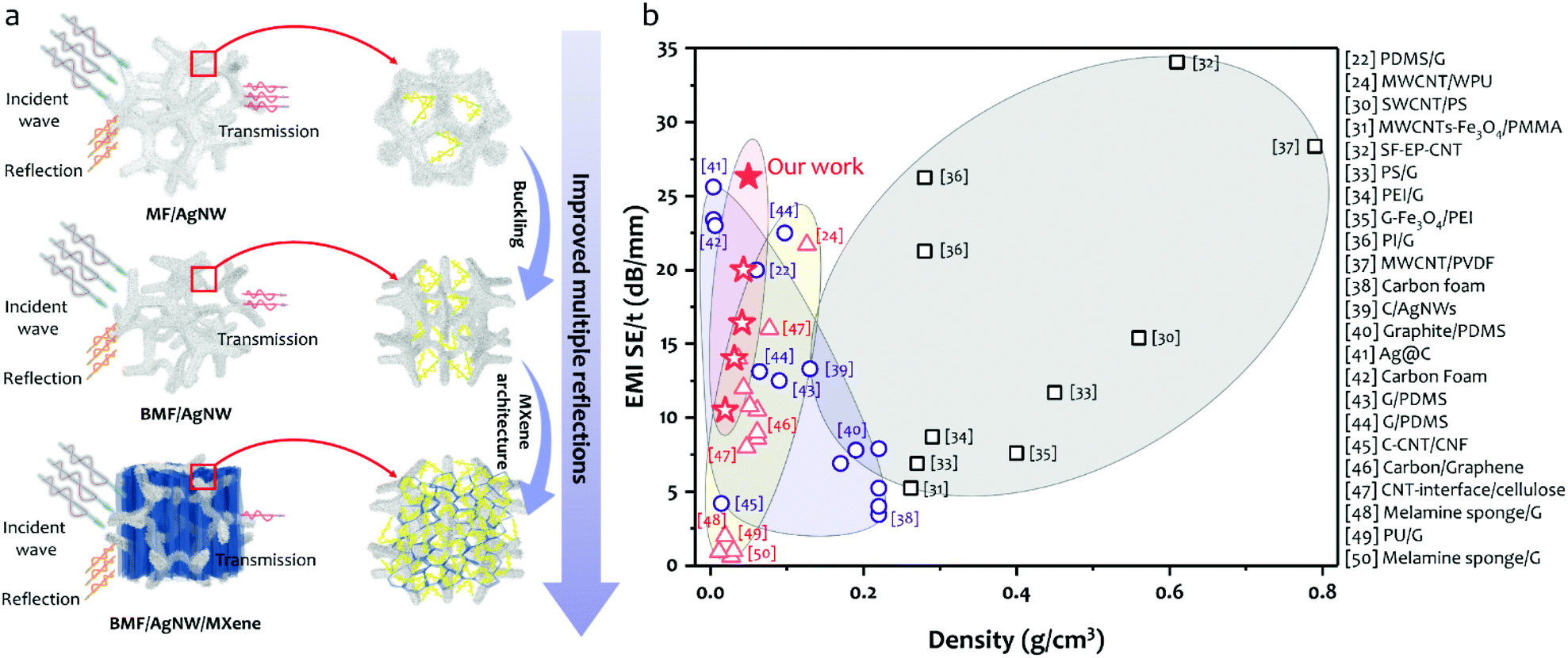
In Fig. 1, the schematic drawing illustrates the fabrication process of a BMF/AgNW/MXene hybrid sponge, including the following two steps. (i) Preparation of the BMF/AgNW sponge (Fig. 1a→c). Firstly, the commercially available open-cell MF sponge is subjected to a triaxial compression along three orthogonal directions with the same compression ratios (more details in Experimental section 4.1 and the hot-pressing mold in Fig. S1†).51–55 The BMF sponge can maintain a compressed configuration during a heating and cooling process, and the buckled microstructure can be regarded as a re-entrant structure, as evidenced by the scanning electron microscopy (SEM) images shown in Fig. 2. We then follow the dip-coating method to coat the polydopamine (PDA) layer and AgNW layer on the backbone of the BMF sponge sequentially. Here, the mussel-inspired PDA serves as a surface modifier due to its abundant catechol and amine groups that may strengthen the adhesion between the AgNW and the surface of the sponge skeleton.56–58 The AgNW is coated through multiple dip-coating cycles in the AgNW suspension (with a concentration of 5 mg ml−1, the typical length of the AgNW is about 41.8 ± 16.2 μm and the diameter is about 73.8 ± 16.0 nm, the detailed information is shown in Fig. S2†). (ii) Incorporation of MXene sheets into the BMF/AgNW sponge to fabricate the hybrid BMF/AgNW/MXene sponge (Fig. 1d→f). Here, we employ a unidirectional freeze-drying method to further build MXene based porous architectures within the BMF/AgNW sponge pores. The as-prepared BMF/AgNW sponge is immersed in the MXene aqueous suspension (with a concentration of 5 mg ml−1, the thickness of the MXene sheet is ∼2.6 nm, and the lateral size is about 2.1 ± 0.8 μm, the detailed information is in Fig. S3†), and then the sample is taken out of a beaker, and placed on a metal disk with a low-temperature cold source of liquid nitrogen. After the sample is totally frozen, it is transferred into a freeze-drying machine to remove the ice template, and the BMF/AgNW/MXene sponge is obtained.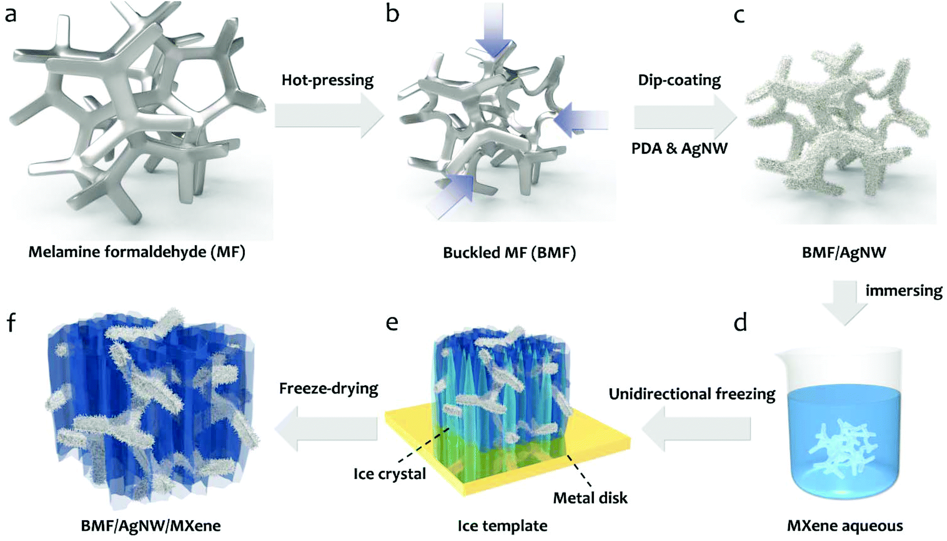 | ||
| Fig. 1 Schematic illustrating the fabrication process of the BMF/AgNW/MXene hybrid sponge by a combination of mechanical hot-pressing (a→b), dip-coating (b→c), immersing (c→d), unidirectional freezing (d→e), and freeze-drying (e→f). | ||
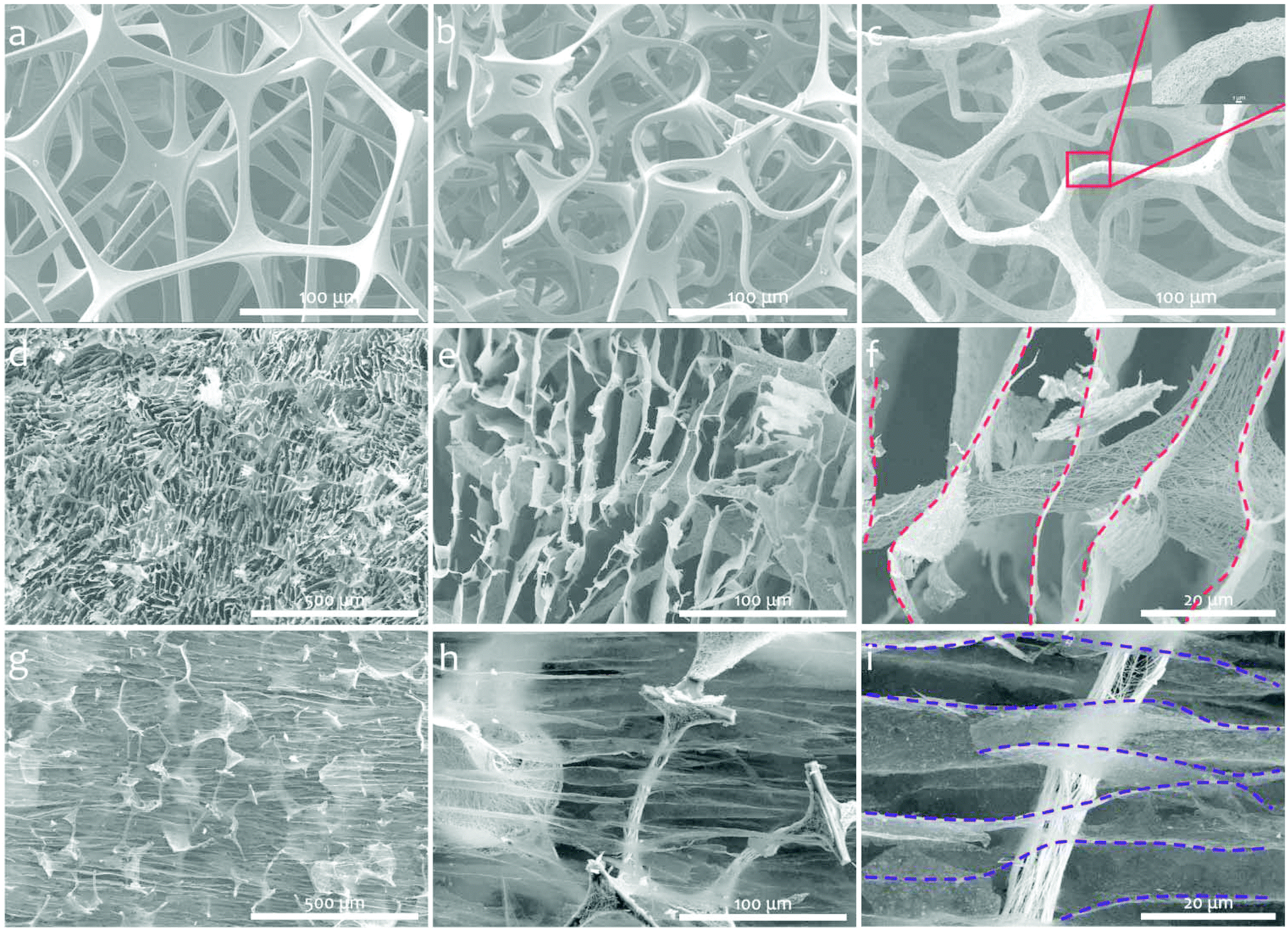 | ||
| Fig. 2 Microstructure of the sponges. SEM images of (a) MF, (b) BMF, and (c) BMF/AgNW sponge, respectively. Inset: Magnified SEM image of c. The SEM images of the BMF/AgNW/MXene sponge along the (d–e) out-of-plane direction and (g–i) in-plane direction under different magnifications (dash lines represent MXene nanosheet assembled cell walls). | ||
SEM is employed to characterize the microstructures of MF, BMF, BMF/AgNW and BMF/AgNW/MXene sponges. Clearly, the polygon-like skeleton forms a continuous network in the MF sponge (Fig. 2a), and it is randomly buckled in the BMF sponge in response to triaxial compression (Fig. 2b). The density of the BMF sponge would increase up to 25.3 mg cm−3 due to the condensed skeletons in the scaffold in comparison with that of MF (7.5 mg cm−3). The inset of the SEM image in Fig. 2c shows the reliable attachment of AgNWs on the skeleton of the BMF sponge. As expected, the electrical conductivity of the as-prepared BMF/AgNW samples shows dependence on the dip-coating cycles (Fig. 3a). We note that the AgNW adsorbed onto the skeleton continuously at early dip-coating cycles, and resulted in the increase of density and conductivity. With further increasing dip-coating cycles, the conductivity reached a plateau. The slightly increased conductivity from 15.3 S cm−1 to 18.0 S cm−1 is accompanied by apparently increased sponge density from 43.0 mg cm−3 to 58.0 mg cm−3. The inset image in Fig. 3a shows the uniformly covered AgNWs onto the skeleton after 4th dip-coating. By balancing the density–electrical conductivity trade-off, finally, a 4-cycle coating procedure is employed to prepare the BMF/AgNW sample.
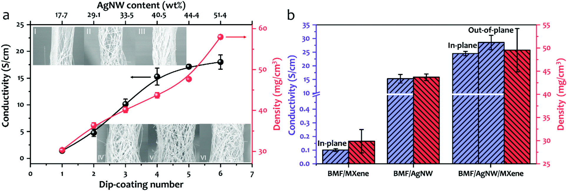 | ||
| Fig. 3 (a) Conductivity and mass density of the BMF/AgNW sponge at different dip-coating cycles. Insets are SEM images of AgNW coated backbone of the BMF sponge. (b) The comparison of conductivity and mass density of BMF/MXene, BMF/AgNW and BMF/AgNW/MXene sponges. | ||
In order to introduce more internal surface areas within the BMF/AgNW sponge, we use two-dimensional (2D) MXene nanosheets as building blocks to fabricate a AgNW/MXene hybrid sponge with a hierarchical structure by a unidirectional freeze-drying method. As shown in Fig. 2d–i, the SEM images of the BMF/AgNW/MXene sponge along the out-of-plane direction and in-plane direction exhibit anisotropic structural features, transverse irregular honeycomb-like morphology and longitudinal channel-like morphology. The MXene nanosheets are well interwoven and stacked within the cell walls to form an interconnected network structure inside the BMF sponge pores. The dash lines in Fig. 2f and i highlight the continuity of MXene cell walls across the AgNW coated BMF skeletons. The ultra-thinness of MXene cell walls (∼90 nm, shown in Fig. S4†) together with extra-high porosity result in the sponge showing a small increase in mass density from 43.0 mg cm−3 to 49.5 mg cm−3, accompanied by increased electrical conductivity up to 24.5 S cm−1 (along the in-plane direction), as shown in Fig. 3b. The electrical conductivity (28.5 S cm−1) in the out-of-plane direction is slightly higher than that in the in-plane direction. The increment in conductivity may be due to the bicontinuous conductive networks derived from the AgNW scaffold and interwoven MXene architecture. For comparison, the pure BMF/MXene sponge was prepared by the unidirectional freeze-drying method (in Fig. S5†). The electrical conductivity of the BMF/MXene sponge (in Fig. 3b) is ∼0.1 S cm−1 along the in-plane direction.
We have characterized the EMI shielding effectiveness of our samples. To highlight the effect of the re-entrant structure on EMI shielding performance, here, we compare four types of BMF/AgNW sponges compressed under different volume ratios, 100% V0 (V0: the initial volume of the MF sponge), 51.2% V0, 42.2% V0 and 29.6% V0. Apparently, the triaxial compression can slightly decrease the porosity of the MF sponge from initial 99.5% to 98.4% in response to the 29.6% V0 volume ratio (as shown in Fig. S6†), accompanied by the increased density from 7.5 mg cm−3 to 25.3 mg cm−3. Fig. 4a shows that, given the very close electrical conductivity, the sponges with buckled structures present better EMI shielding performances than the pristine one in the X band (8.2–12.4 GHz). The EMI shielding effectiveness shows positive dependence on the applied volume ratios and reaches the maximum at 29.6% V0. Due to the obvious enhancement in the surface/interface area in the buckled sponge in comparison with the pristine sponge, more multiple reflections are expected to occur at interfaces, and eventually lead to an improved EMI shielding effectiveness when the incident EM waves are in contact with the sponge. After the introduction of hierarchical MXene cell walls inside the sponge pores in the BMF/AgNW sample, significantly improved EMI shielding effectiveness up to 52.6 dB is observed as shown in Fig. 4b. Comparatively, the EMI shielding effectiveness of the BMF/MXene sponge is around 40.0 dB (at 8.2 GHz). It is worth noting that the EMI shielding performance of the BMF/AgNW/MXene and BMF/MXene sponges was measured along the in-plane direction. The reason is related to the fact that the more multi-reflections occurred once the incident electromagnetic waves propagated along the in-plane direction in the anisotropic porous structures.59
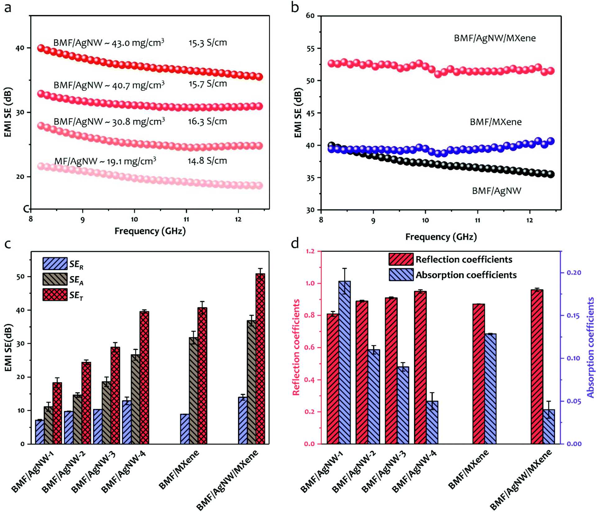 | ||
| Fig. 4 (a) The EMI SE (X band) of MF/AgNW and BMF/AgNW sponges compressed with different volume ratios. (b) The comparison of EMI SE between BMF/MXene, BMF/AgNW and BMF/AgNW/MXene sponges. (c) Average SET, SER and SEA values of the various BMF/AgNW sponges having different conductivities, BMF/MXene, and BMF/AgNW/MXene at 8.2 GHz, and (d) the corresponding average R and A values. | ||
The total EMI shielding effectiveness (SET) usually includes the absorption of electromagnetic waves (SEA), the reflection from materials (SER) and the multiple reflections in the interior of materials (SEMR). The multiple reflection loss happens when the representative materials are porous and can be ignored when SET > 15 dB.22 In Fig. 4c, the average SET, SEA and SER (at 8.2 GHz) of BMF/AgNW samples with different AgNW loading contents, BMF/MXene, and BMF/AgNW/MXene samples are listed. As expected, the SET increases monotonically with increasing electrical conductivity of BMF/AgNW samples. Specifically, the BMF/AgNW-1 (1 denotes one cycle of AgNW coating) sponge with an electrical conductivity of 1.4 S cm−1 exhibits a SET of 17.0 dB (at 8.2 GHz), whereas the BMF/AgNW-4 sponge (conductivity: 15.3 S cm−1) presents a SET of 40.0 dB (at 8.2 GHz). Surprisingly, even with the lowest conductivity (0.1 S cm−1) among the tested samples, the BMF/MXene exhibits a relatively larger SEA (31.8 dB) in comparison with all the BMF/AgNW samples, implying the considerable contribution of MXene cell walls to the EM shielding performance. Furthermore, the BMF/AgNW/MXene shows the highest SEA of 36.8 dB, and leads to the best shielding performance in terms of SET.
In order to figure out the underlying mechanism of EMI shielding for our samples, we calculate the corresponding power coefficients R (reflection) and A (absorption) from the measured S parameters that can evaluate the power balance of electromagnetic waves interacting with sponges in Fig. 4d. We find that R contributes more than 80% for all sponges even though these sponges are of higher SEA values, and reaches a value of 96% for the BMF/AgNW/MXene sponge. This phenomenon can be explained by the fact that the reflection of an incident electromagnetic wave happens before the absorption while the remaining electromagnetic wave enters the interior and generates absorption and multiple reflections, due to the impedance mismatches between the shielding materials and free space.41,60 Therefore, the highest conductivity (24.5 S cm−1) of BMF/AgNW/MXene results in larger impedance mismatches and exhibits a higher R value, and the remaining electromagnetic wave enters the hierarchical BMF/AgNW/MXene sponge and leads to absorption and multiple reflections with a SEA value of 36.8 dB.
In Fig. 5a, we discuss possible shielding mechanisms for our three types of as-prepared sponges. For the BMF/AgNW sponge, the enhanced surface area due to mechanical compression would lead to more multiple reflections and scattering of EM waves at the cell–matrix interfaces with impedance mismatch, thereby resulting in higher EMI shielding effectiveness. Comparatively, the BMF/AgNW/MXene sponge, containing both the AgNW scaffold and irregular honeycomb-like MXene architecture, leads to sufficient multiple reflections and scattering due to the presence of MXene nanosheet assembled cell walls, and finally realizes the attenuation of EM energy by both conductive dissipation and multiple reflections and scattering during EM shielding. Based on the results in Fig. 4, we thus suggest that the good EMI shielding effectiveness of the BMF/AgNW/MXene sponge is attributed to the synergistic effect in both improvements of conductivity and hierarchical structure, where the high conductivity of the hybrid AgNW/MXene network would contribute to impedance mismatches between the sponge and free space, and the AgNW scaffold and irregular honeycomb-like MXene architecture may further cause substantial internal interface multi-reflections and scattering as compared with the neat BMF/AgNW sponge.
 | ||
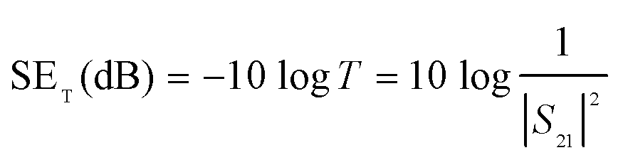
| Fig. 5 (a) Schematic illustration of EMI shielding mechanisms for MF/AgNW, BMF/AgNW and BMF/AgNW/MXene sponges, respectively. (b) Comparison of EMI SE of different nanomaterial-based EMI materials as a function of density. (Square: foaming & phase separating method. Circle: carbonizing & CVD method. Triangle: freeze-drying & dip-coating. Hollow stars: BMF/AgNW with different densities. Solid star: BMF/AgNW/MXene. G: graphene; CNT: carbon nanotube; SF: silver plating foam; EP: epoxy; PS: polystyrene; PVDF: polyvinylidene fluoride; PI: polyimide; WPU: water polyurethane; PEI: polyetherimide; PMMA: polymethyl methacrylate.) | ||
Finally, we did a comprehensive comparison with previously reported EMI materials summarized in Fig. 5b.22,24,30–50 Examples include nanocarbon- and nanometal-based foams while the bulky carbon- or metal-based EMI shielding materials are not considered here due to their relatively large mass density (>1 g cm−3).61 The detailed data about the comparison of EMI SE versus density are summarized in Table S1 in the ESI.† Following the literature, we plot EMI SE divided by the thickness (t) of the shielding materials against the mass density of various samples. Based on the difference in preparation methods, these materials are divided into three groups: foaming & phase separating (grey-shaded), carbonizing & CVD (blue-shaded) and template (dip-coating and freeze-drying, yellow-shaded). EMI shielding materials based on the foaming & phase separating method typically produce high shielding effectiveness but with high density in a range from ∼200 mg cm−3 to 800 mg cm−3. For materials based on carbonizing & CVD methods, although both the high shielding effectiveness and low density down to several tens of mg cm−3 can be achieved, the limitation in sample sizes further greatly hinders its large-scale practical application. In comparison, the BMF/AgNW sponges with the lower mass density in a range from 19.1 mg cm−3 to 43.0 mg cm−3 exhibit relatively poor specific EMI SE values ranging from 10.5 dB mm−1 to 20 dB mm−1 in Fig. 5b (hollow stars) due to the limitation in surface areas. After the introduction of the MXene architecture into the BMF/AgNW sponge, the apparent improvement in EMI SE (solid star in Fig. 5b) is observed. Therefore, the resulting high-performance EMI shielding and low-density BMF/AgNW/MXene sponge based on the buckled AgNW scaffold and irregular honeycomb-like MXene architecture by the combination of dip-coating and freeze-drying has highlighted hierarchical structure advantage.
3. Conclusions
In conclusion, a low-density and conductive AgNW/MXene hybrid EMI shielding sponge with high EMI shielding performance is demonstrated in this work. Importantly, the sponges enabled by a novel buckling design exhibit a conductivity of up to 15.3 S cm−1 and superior EMI shielding effectiveness above 40.0 dB in the X-band, and the density as low as 43.0 mg cm−3. Furthermore, after the introduction of an irregular honeycomb-like MXene architecture, an EMI shielding effectiveness of 52.6 dB together with an apparent improvement in conductivity to 24.5 S cm−1 is achieved at a density of 49.5 mg cm−3. These outstanding performances of our sponges highlight the advantages of buckled structures and the synergistic effect of AgNW and MXene both in conductivity and hierarchical structures. In addition, the combination of dip-coating and freeze-drying may be extended to other nanomaterials for high-performance EMI shielding applications.4. Experimental section
4.1 Preparation of BMF sponge
The commercially available open-cell MF sponges were cut into small pieces (45 × 45 × 30 mm3), then cleaned with ethanol and deionized water and dried in the oven for later use. Here we have designed three different sizes of molds to control the buckled structure, and the MF sponges were compressed triaxially. The compression ratio was the same in all three orthogonal directions, and the compression ratio is defined as the ratio of the volume (V0: the volume of the MF sponge), and the ratio can be calculated as BMF-1 (51.2% V0), BMF-2 (42.2% V0) and BMF-3 (29.6% V0), respectively. The molds were then put in the hot press machine under pressure at 180 °C and kept for 1 h. After that, the sponges were taken out and cooled to room temperature, and then removed from the molds and cleaned.4.2 Preparation of PDA modified BMF sponge
Firstly, tris(hydroxymethyl) aminomethane (0.242 g) was added into 200 ml distilled water, and the pH value was adjusted to 8.5 using HCl. After that, dopamine hydrochloride (0.2 g) was added and dissolved under magnetic stirring. The cleaned BMF sponges were cut into small pieces and dipped into the above solution overnight, and then picked out and dried at 40 °C.4.3 Synthesis of AgNW
The AgNW was synthesized as follows.62,63 Firstly, PVP (6 g, MW = 300![[thin space (1/6-em)]](https://www.rsc.org/images/entities/char_2009.gif) 000) was added to 150 ml of ethylene glycol (EG) and wholly dissolved. Secondly, 5 g of silver nitrate (AgNO3) was added to the above PVP/EG solution and completely dissolved. Thirdly, 20 g of a CuCl2 salt solution (50 mM in EG) was carefully dumped into the mixture and stirred. Finally, the mixture was then transferred to the oil bath at 130 °C. After the synthesizing process, acetone and ethanol were used to wash the precipitate.
000) was added to 150 ml of ethylene glycol (EG) and wholly dissolved. Secondly, 5 g of silver nitrate (AgNO3) was added to the above PVP/EG solution and completely dissolved. Thirdly, 20 g of a CuCl2 salt solution (50 mM in EG) was carefully dumped into the mixture and stirred. Finally, the mixture was then transferred to the oil bath at 130 °C. After the synthesizing process, acetone and ethanol were used to wash the precipitate.
4.4 Synthesis of MXene
MXene was synthesized by selectively etching Al from the MAX phase (Ti3AlC2, 400 mesh, purchased from Jilin 11 Technology Co., Ltd). In a typical etching method,64 3.2 g LiF was dissolved in 40 ml of 9 M HCl in a Teflon container and further magnetically stirred for 30 min to form a homogeneous etchant solution. This was followed by the gradual addition of 2 g Ti3AlC2 powder, and the reaction mixture was kept at 35 °C with continuous stirring for 24 h. Afterward, the obtained mixture solution was washed with H2O with centrifugation and shaking until the pH of the dispersion was near neutral (3500 rpm, 5 min). After that, the obtained sediment was dispersed in H2O and bath sonicated for 30 min, followed by centrifugation for 1 h (3500 rpm). And the supernatant was collected for the preparation of composite films in this work.4.5 Preparation of BMF/AgNW sponge
The modified BMF sponges were immersed in the AgNW dispersion for 30 min, and the excess AgNW was blown away by nitrogen. The dip-coating process was repeated until the surface of BMF was fully coated, and the resulting AgNW sponge was dried overnight.4.6 Preparation of BMF/AgNW/MXene sponge
The prepared BMF/AgNW sponge was immersed in the MXene solution (5 mg ml−1), followed by unidirectional freezing with a Teflon container and stainless steel bottom in liquid nitrogen, and then put in the freeze-drying machine for 24 h to obtain the BMF/AgNW/MXene sponge.4.7 Characterization
The morphologies of sponges were examined by using a scanning electron microscope (JEOL JSM-7500F). The electrical resistance of BMF/AgNW and BMF/AgNW/MXene sponges was measured by using a Keithley 4200 SourceMeter through the four wire probe method.4.8 Electromagnetic shielding effectiveness of BMF/AgNW and BMF/AgNW/MXene sponges
EMI SE characterization was carried out through the waveguide method by using a vector network analyzer (Agilent E8363B PNA-L) in the frequency range of 8.2–12.4 GHz (X-band). The size of the samples is 22.86 × 10.16 mm2, and the thickness of the sample is 2 mm. More than four samples were prepared for EMI testing for the statistic average. The S parameters of each sample were recorded, and the EMI SE was calculated by using the following formulas.| R = |S11| T = |S21|2 A + T + R = 1 |
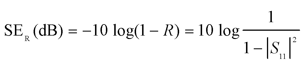
| SEA(dB) = SET − SER |
Conflicts of interest
There are no conflicts to declare.Acknowledgements
We thank Dr Zhihui Zeng for fruitful discussion. This project was jointly supported by the National Natural Science Foundation of China (Grant No. 21474023, 11890682 and 11832010) and the National Key Basic Research Program of China (Grant No. 2013CB934203).References
- B. Wen, M. Cao, M. Lu, W. Cao, H. Shi, J. Liu, X. Wang, H. Jin, X. Fang, W. Wang and J. Yuan, Adv. Mater., 2014, 26, 3484–3489 CrossRef CAS PubMed.
- X. P. Zhang, L. C. Jia, G. Zhang, D. X. Yan and Z. M. Li, J. Mater. Chem. C, 2018, 6, 10760–10766 RSC.
- L.-C. Jia, W.-J. Sun, C.-G. Zhou, D.-X. Yan, Q.-C. Zhang and Z.-M. Li, J. Mater. Chem. C, 2018, 6, 9166–9174 RSC.
- X. Shui and D. D. L. Chung, J. Electron. Mater., 1997, 26, 928–934 CrossRef CAS.
- H. Abbasi, M. Antunes and J. I. Velasco, Prog. Mater. Sci., 2019, 103, 319–373 CrossRef CAS.
- S. Stankovich, D. A. Dikin, G. H. Dommett, K. M. Kohlhaas, E. J. Zimney, E. A. Stach, R. D. Piner, S. T. Nguyen and R. S. Ruoff, Nature, 2006, 442, 282–286 CrossRef CAS.
- V. P. Veedu, A. Cao, X. Li, K. Ma, C. Soldano, S. Kar, P. M. Ajayan and M. N. Ghasemi-Nejhad, Nat. Mater., 2006, 5, 457–462 CrossRef CAS PubMed.
- Y.-X. Fu, Z.-X. He, D.-C. Mo and S.-S. Lu, Int. J. Therm. Sci., 2014, 86, 276–283 CrossRef CAS.
- Z. Zeng, S. I. Seyed Shahabadi, B. Che, Y. Zhang, C. Zhao and X. Lu, Nanoscale, 2017, 9, 17396–17404 RSC.
- Y. Li, S. Wang, Q. Peng, Z. Zhou, Z. Yang, X. He and Y. Li, Nanoscale, 2019, 11, 16384–16392 RSC.
- Y. Li, L. Sun, F. Xu, S. Wang, Q. Peng, Z. Yang, X. He and Y. Li, Nanoscale, 2019, 11, 1692–1699 RSC.
- M. Chen, L. Zhang, S. Duan, S. Jing, H. Jiang, M. Luo and C. Li, Nanoscale, 2014, 6, 3796–3803 RSC.
- B. Wen, X. X. Wang, W. Q. Cao, H. L. Shi, M. M. Lu, G. Wang, H. B. Jin, W. Z. Wang, J. Yuan and M. S. Cao, Nanoscale, 2014, 6, 5754–5761 RSC.
- Y. Wang, F. Q. Gu, L. J. Ni, K. Liang, K. Marcus, S. L. Liu, F. Yang, J. J. Chen and Z. S. Feng, Nanoscale, 2017, 9, 18318–18325 RSC.
- L.-C. Jia, L. Xu, F. Ren, P.-G. Ren, D.-X. Yan and Z.-M. Li, Carbon, 2019, 144, 101–108 CrossRef CAS.
- P. Li, D. Du, L. Guo, Y. Guo and J. Ouyang, J. Mater. Chem. C, 2016, 4, 6525–6532 RSC.
- J. Lyu, X. Zhao, X. Hou, Y. Zhang, T. Li and Y. Yan, Compos. Sci. Technol., 2017, 149, 159–165 CrossRef.
- M. Crespo, M. González, A. L. Elías, L. P. Rajukumar, J. Baselga, M. Terrones and J. Pozuelo, Phys. Status Solidi RRL, 2014, 8, 698–704 CrossRef CAS.
- D. Lu, Z. Mo, B. Liang, L. Yang, Z. He, H. Zhu, Z. Tang and X. Gui, Carbon, 2018, 133, 457–463 CrossRef CAS.
- S. Zhao, Y. Yan, A. Gao, S. Zhao, J. Cui and G. Zhang, ACS Appl. Mater. Interfaces, 2018, 10, 26723–26732 CrossRef CAS PubMed.
- J. B. Xi, Y. L. Li, E. Z. Zhou, Y. J. Liu, W. W. Gao, Y. Guo, J. Ying, Z. C. Chen, G. G. Chen and C. Gao, Carbon, 2018, 135, 44–51 CrossRef CAS.
- Z. Chen, C. Xu, C. Ma, W. Ren and H. M. Cheng, Adv. Mater., 2013, 25, 1296–1300 CrossRef CAS PubMed.
- Q. Song, F. Ye, X. Yin, W. Li, H. Li, Y. Liu, K. Li, K. Xie, X. Li, Q. Fu, L. Cheng, L. Zhang and B. Wei, Adv. Mater., 2017, 29, 1701583 CrossRef PubMed.
- Z. H. Zeng, H. Jin, M. J. Chen, W. W. Li, L. C. Zhou and Z. Zhang, Adv. Funct. Mater., 2016, 26, 303–310 CrossRef CAS.
- Z. Zeng, H. Jin, M. Chen, W. Li, L. Zhou, X. Xue and Z. Zhang, Small, 2017, 13, 1701388 CrossRef PubMed.
- Y. Xu, Y. Li, W. Xu and J. Bao, J. Mater. Sci.: Mater. Electron., 2014, 26, 1159–1171 CrossRef.
- M. Hamidinejad, B. Zhao, A. Zandieh, N. Moghimian, T. Filleter and C. B. Park, ACS Appl. Mater. Interfaces, 2018, 10, 30752–30761 CrossRef CAS PubMed.
- B. Shen, Y. Li, D. Yi, W. Zhai, X. Wei and W. Zheng, Carbon, 2016, 102, 154–160 CrossRef CAS.
- D. D. L. Chung, Carbon, 2001, 39, 279–285 CrossRef CAS.
- Y. Yang, M. C. Gupta, K. L. Dudley and R. W. Lawrence, Nano Lett., 2005, 5, 2131–2134 CrossRef CAS PubMed.
- H. Zhang, G. Zhang, J. Li, X. Fan, Z. Jing, J. Li and X. Shi, Composites, Part A, 2017, 100, 128–138 CrossRef CAS.
- Y. Xu, Y. Li, W. Hua, A. Zhang and J. Bao, ACS Appl. Mater. Interfaces, 2016, 8, 24131–24142 CrossRef CAS PubMed.
- D.-X. Yan, P.-G. Ren, H. Pang, Q. Fu, M.-B. Yang and Z.-M. Li, J. Mater. Chem., 2012, 22, 18772–18774 RSC.
- J. Ling, W. Zhai, W. Feng, B. Shen, J. Zhang and W. Zheng, ACS Appl. Mater. Interfaces, 2013, 5, 2677–2684 CrossRef CAS.
- B. Shen, W. Zhai, M. Tao, J. Ling and W. Zheng, ACS Appl. Mater. Interfaces, 2013, 5, 11383–11391 CrossRef CAS.
- Y. Li, X. L. Pei, B. Shen, W. T. Zhai, L. H. Zhang and W. G. Zheng, RSC Adv., 2015, 5, 24342–24351 RSC.
- H. Wang, K. Zheng, X. Zhang, X. Ding, Z. X. Zhang, C. Bao, L. Guo, L. Chen and X. Y. Tian, Compos. Sci. Technol., 2016, 125, 22–29 CrossRef CAS.
- Y. Yuan, Y. Ding, C. Wang, F. Xu, Z. Lin, Y. Qin, Y. Li, M. Yang, X. He, Q. Peng and Y. Li, ACS Appl. Mater. Interfaces, 2016, 8, 16852–16861 CrossRef CAS PubMed.
- Y. Yuan, X. Sun, M. Yang, F. Xu, Z. Lin, X. Zhao, Y. Ding, J. Li, W. Yin, Q. Peng, X. He and Y. Li, ACS Appl. Mater. Interfaces, 2017, 9, 21371–21381 CrossRef CAS PubMed.
- H. Li, L. Jing, Z. L. Ngoh, R. Y. Tay, J. Lin, H. Wang, S. H. Tsang and E. H. T. Teo, ACS Appl. Mater. Interfaces, 2018, 10, 41707–41716 CrossRef CAS PubMed.
- Y. J. Wan, P. L. Zhu, S. H. Yu, R. Sun, C. P. Wong and W. H. Liao, Small, 2018, 14, 1800534 CrossRef PubMed.
- Y. Tang, D. Li, D. Ao, S. Li and X. Zu, J. Mater. Sci.: Mater. Electron., 2018, 29, 13643–13652 CrossRef CAS.
- X. Y. Sun, X. Liu, X. Shen, Y. Wu, Z. Y. Wang and J. K. Kim, Composites, Part A, 2016, 85, 199–206 CrossRef CAS.
- L. Kong, X. W. Yin, M. K. Han, X. Y. Yuan, Z. X. Hou, F. Ye, L. T. Zhang, L. F. Cheng, Z. W. Xu and J. F. Huang, Carbon, 2017, 111, 94–102 CrossRef CAS.
- O. Pitkanen, J. Tolvanen, I. Szenti, A. Kukovecz, J. Hannu, H. Jantunen and K. Kordas, ACS Appl. Mater. Interfaces, 2019, 11, 19331–19338 CrossRef CAS PubMed.
- Y. Yuan, L. Y. Liu, M. L. Yang, T. L. Zhang, F. Xu, Z. S. Lin, Y. J. Ding, C. H. Wang, J. J. Li, W. L. Yin, Q. Y. Peng, X. D. He and Y. B. Li, Carbon, 2017, 123, 223–232 CrossRef CAS.
- L. Q. Zhang, S. G. Yang, L. Li, B. Yang, H. D. Huang, D. X. Yan, G. J. Zhong, L. Xu and Z. M. Li, ACS Appl. Mater. Interfaces, 2018, 10, 40156–40167 CrossRef CAS PubMed.
- C. Liu, S. Ye and J. Feng, Chem. – Asian J., 2016, 11, 2586–2593 CrossRef CAS PubMed.
- B. Shen, Y. Li, W. Zhai and W. Zheng, ACS Appl. Mater. Interfaces, 2016, 8, 8050–8057 CrossRef CAS PubMed.
- T. Guo, X. Chen, L. Su, C. Li, X. Huang and X.-Z. Tang, Mater. Des., 2019, 182, 108029 CrossRef CAS.
- R. Lakes, Science, 1987, 235, 1038–1041 CrossRef CAS PubMed.
- Z. Dai, C. Weng, L. Liu, Y. Hou, X. Zhao, J. Kuang, J. Shi, Y. Wei, J. Lou and Z. Zhang, Sci. Rep., 2016, 6, 32989 CrossRef CAS PubMed.
- Y. Li, S. D. Luo, M. C. Yang, R. Liang and C. C. Zeng, Adv. Funct. Mater., 2016, 26, 2900–2908 CrossRef CAS.
- C. Weng, Z. Dai, G. Wang, L. Liu and Z. Zhang, ACS Appl. Mater. Interfaces, 2019, 11, 6541–6549 CrossRef CAS PubMed.
- C. Yang and S. Kyriakides, Int. J. Solids Struct., 2019, 159, 239–256 CrossRef CAS.
- H. Lee, S. M. Dellatore, W. M. Miller and P. B. Messersmith, Science, 2007, 318, 426–430 CrossRef CAS.
- H. Lee, Y. Lee, A. R. Statz, J. Rho, T. G. Park and P. B. Messersmith, Adv. Mater., 2008, 20, 1619–1623 CrossRef CAS.
- S. M. Kang, S. Park, D. Kim, S. Y. Park, R. S. Ruoff and H. Lee, Adv. Funct. Mater., 2011, 21, 108–112 CrossRef CAS.
- Z. Zeng, M. Chen, Y. Pei, S. I. Seyed Shahabadi, B. Che, P. Wang and X. Lu, ACS Appl. Mater. Interfaces, 2017, 9, 32211–32219 CrossRef CAS.
- Z. H. Zeng, M. J. Chen, H. Jin, W. W. Li, X. Xue, L. C. Zhou, Y. M. Pei, H. Zhang and Z. Zhang, Carbon, 2016, 96, 768–777 CrossRef CAS.
- Y. Xu, W. Xu and J. Bao, J. Polym. Res., 2014, 21, 543 CrossRef.
- J. Lee, P. Lee, H. Lee, D. Lee, S. S. Lee and S. H. Ko, Nanoscale, 2012, 4, 6408–6414 RSC.
- J. Jiu, T. Araki, J. Wang, M. Nogi, T. Sugahara, S. Nagao, H. Koga, K. Suganuma, E. Nakazawa, M. Hara, H. Uchida and K. Shinozaki, J. Mater. Chem. A, 2014, 2, 6326–6330 RSC.
- M. Alhabeb, K. Maleski, B. Anasori, P. Lelyukh, L. Clark, S. Sin and Y. Gogotsi, Chem. Mater., 2017, 29, 7633–7644 CrossRef CAS.
Footnote |
| † Electronic supplementary information (ESI) available. See DOI: 10.1039/c9nr07988b |
| This journal is © The Royal Society of Chemistry 2019 |