
High-performance self-powered perovskite photodetector with a rapid photoconductive response†
Kavita Pandey,
Mihirsinh Chauhan,
Vishwa Bhatt,
Brijesh Tripathi,
Pankaj Yadav* and
Manoj Kumar *
*
School of Technology, Pandit Deendayal Petroleum University, Gandhinagar – 382007, India. E-mail: manoj.kspv@gmail.com; pankajphd11@gmail.com
First published on 13th October 2016
Abstract
Here we report the development of a self-powered high-speed perovskite Schottky junction photodiode, which is very important for next-generation electronic devices. The ITO/perovskite Schottky junction diode yielded a rectification behaviour with a low value of reverse saturation current under dark conditions, and a zero bias photocurrent when illuminated. The fabricated photodiode exhibited a high photosensitivity with fast response and recovery times. The origin of the high photocurrent in the fabricated photodiode was analysed by making a log–linear plot of its current–voltage characteristics. The study also demonstrated the efficient charge transport properties of the CH3NH3Pbl3 semiconductor material with the photogenerated electrons injected into the ITO contact and the holes injected into the gold contact. The obtained results provide a way to fabricate an efficient self-bias photodiode for future electronic devices.
Introduction
Photodetectors are currently the most important functional components of image sensors used in digital cameras and smart phones, and for optical communication.1–3 Recently, semiconductors such as Si, GaN, ZnO, SnO2, CdS and TiO2 have gained significant research attention with regards to their application in photodetectors.4–7 These materials are mainly used in heterojunction and Schottky junction configurations with their electrical performance in photovoltaic and photoconductive modes. But the presence of many internal and surface defects in photodetectors based on these semiconductors has been shown to yield slow responses and short lifetimes.8,9Organohalide lead is a new type of optoelectronic material that has been applied in photovoltaics, phototransistors, light emitting diodes (LEDs) and photodetectors, and has received major research attention.10–13 Perovskite materials display electrical and optical properties such as low excitonic binding energy, high mobility, long charge carrier lifetime and diffusion length, durable band gap and ultrafast charge generation, and these properties have been shown to be favourable for optoelectronics application.14–16 The favourability of these properties has been demonstrated by the attainment of efficiency values greater than 20% in the photovoltaic mode within a few years of the development of such applications.17,18 Recently, the suitability of perovskite materials for high-performance photodetectors has been demonstrated.19–22 Perovskite materials have shown two advantages over inorganic materials for photodetectors: the presence of dominant intrinsic defects only at shallow levels, allowing for the photoconductivity to persist,23,24 and the possibility of solution and vacuum processing at low temperatures.
Hu et al. demonstrated the fabrication of a CH3NH3PbI3-based photodetector by using a lateral geometry.25 Yang et al. made a sandwich structured photodetector exhibiting fast speed and high responsivity.17 Dong et al. produced a photodetector with a vertical stack type of geometry and showed this photodetector to display a high gain and fast response.26 Banavoth et al. fabricated an air-stable sandwich-type photodetector.27 Dou et al. used solution processing to make a hybrid perovskite photodetector showing high detectivity.21 Most of the reported perovskite-based photodetectors in the literature and discussed above have utilized the perovskite solar structure in principle. However, such a structure is not optimal for photodetectors because (i) the use of electron transport layers (ETLs) and hole transport layers (HTLs) in photodetectors can cause excess capacitance due to the high intrinsic capacitance levels of ETLs and HTLs,28,29 and (ii) the heterojunction formed at the perovskite layer over the mesoporous material can lead to a high interfacial junction area that leads to a high parasitic capacitance.30
Considering the above mentioned shortfalls by introducing HTLs and ETLs to the device structure, the present work is focused on (i) developing an in-depth detailed working mechanism as a function of bias and light based on obtaining net terminal current–voltage characteristics, photodynamic measurements, and band bending and alignment, (ii) demonstrating a low-cost solution-processable technique for the fabrication of a highly efficient zero-biased photodetector, and (iii) demonstrating the capability of a perovskite layer to generate and conduct both electrons and holes under illumination, which is critically important for designing high-speed photodetectors. Our work provided an efficient low-cost method to fabricate and analyze self-biased photodetectors.
Material synthesis and characterization
The detailed steps involved in the fabrication of the active perovskite layer and its structural, morphological and optical properties have been discussed in detail in our previous reports.31–33 The fabrication of the perovskite material is nevertheless briefly summarized here: first, the perovskite sensitizer CH3NH3I was stirred with hydrochloric acid and methylamine for two hours at 0 °C and then transferred to a vapour evaporator for one hour at 50 °C; then, CH3NH3I precipitates were extracted and washed in diethyl ether, and the obtained CH3NH3I (0.125 g) and PbI2 (1.27 g, 99% Aldrich) were mixed and stirred in γ-butyrolactone (2 ml, 99% Aldrich) at 60 °C for 24 hours to prepare CH3NH3PbI3. Indium-doped tin oxide (ITO) glasses were used as substrates and displayed a sheet resistance of 9 Ω cm−2. The as-prepared CH3NH3PbI3 was then spin coated on the ITO glass at 3500 rpm for 45 seconds and sintered at 100 °C for two hours under ambient atmospheric conditions.The photocurrents of the fabricated photodetectors were measured under standard red LED light at 25 °C by using an Agilent 2772 source meter. The photodynamic measurements were taken at room temperature by using a CH Instrument 660D potentiostat equipped with general purpose electrochemical system software.
Results and discussion
Fig. 1A shows the voltage-dependent net terminal current of the ITO/perovskite Schottky junction under dark conditions at room temperature in the applied bias range of −1.5 to 1.5 V. The measured current (Id) in the dark showed a rectification behaviour with an increasing applied bias (V), which confirmed the formation of a junction barrier at the interface between the ITO glasses and perovskite thin films. A forward bias knee voltage or turn-on voltage of the fabricated Schottky junction was found at about 1.3 V, which is comparable to the commonly reported values for wide-bandgap-based p–n junction photodetectors and somewhat higher than those of perovskite heterojunctions.14,19,31–36 The relatively high value of the turn-on voltage in the present case may have been associated with the formation of a relatively good rectifying junction between the ITO glasses and the perovskite semiconductors. The fabricated device showed a rectification ratio of 10 for bias voltages of +1.5 and −1.5 V and a reverse saturation current of 1.7 × 10⁻⁸ A. The obtained values for the reverse saturation current are of the same order of magnitude as those reported for wafers or photodiodes fabricated on glass substrates and previous reports of perovskite photodiodes.31–37 Fig. 1B shows a −dV/dJ plot for the fabricated device under dark conditions. In the bias range where I0 is very small, the net Id, i.e., I0[exp(Vjm−1) − 1] was simplified as Id ≈ ISH − Vj(RSH)−1, where I0 is the reverse saturation current, Vj is the junction voltage and RSH is the shunt resistance of the diode and ISH is the current across the shunt.38 Here, the bias response Id depends upon the value of RSH. The point at which the plotted −dV/dI response plateaus gives an approximate value for RSH. The value of RSH under dark conditions was found to be approximately 1.8 kΩ. In general, to achieve an efficient high-speed photodetector, a high value of RSH is required. Moreover, the value of Rs (series resistance) can be obtained. Fig. 1B shows the response of the photodetector under dark conditions in the voltage-independent region. These data followed a linear trend, in contrast to that shown by the saturated response in the bias-dependent region. By noting the intercept of the plotted data (inset of Fig. 1B), a value of ∼3.8 Ω was obtained for the series resistance. The obtained values of RS here are comparable to those of the previous reports on perovskite Schottky junctions and heterojunctions employed for photovoltaic and photodetector applications.17–20,31–33 Note that the value of RS was due to the ohmic contributions of the ITO glass, gold contacts, and connecting leads of the photodetector, whereas the value of RSH was from the ITO/perovskite interfacial junction.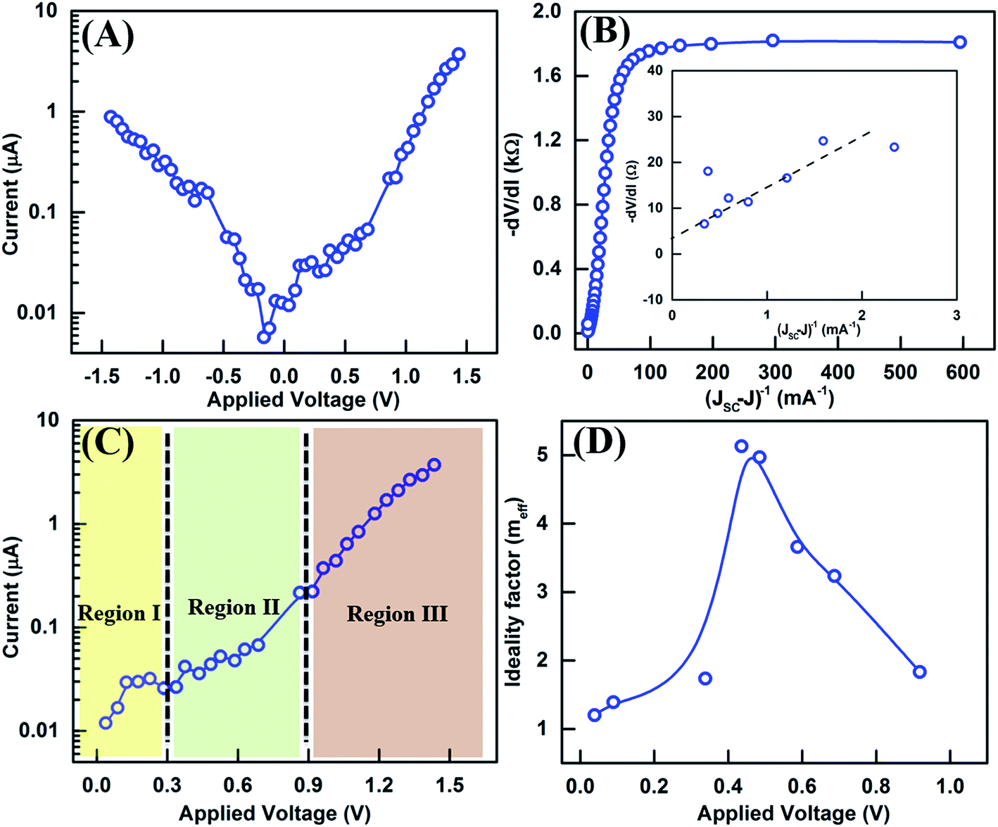 | ||
| Fig. 1 (A) Voltage-dependent net terminal current under dark conditions. (B) Plot of −dV/dL versus (LSC − L)−1 with the linear fitting curves. (C) Forward bias current voltage characteristics under dark conditions. (D) Effective diode ideality factor as a function of junction voltage. | ||
The current–voltage characteristics in a log–linear plot and the effective ideality factor (meff) under dark conditions are shown in Fig. 1C and D, respectively. The obtained current–voltage curves showed distinct behaviors in three different regions, with these behaviors depending upon the dominance of the conduction and recombination mechanisms. In Region I, the current–voltage plot showed an ohmic behaviour with a linear change in current with the applied voltage. The corresponding region in the meff plot showed a value of meff < 1.5. The physical significance of the behavior in Region I has been widely explained for photovoltaic devices.39 The current–voltage curve in Region II showed an exponential response (I ∝ exp(V)), which generally characterizes the conduction mechanism of recombination tunnelling.40,41 The higher value of meff in Region II than in Region I signified a high carrier injection and recombination, which led to the higher current gain. In the probed bias region, a narrowing of the space charge region occurred, as a result of the applied bias and increased charge carrier density, which caused a narrowing of the space charge region. The narrowing of the space charge region permitted further tunnelling of carriers across the junction, thus increasing the net terminal current and photocurrent gain. The formation of a space charge region and a space charge limited current (SCLC) conduction mechanism has been common observations for heterojunctions.42 Region III of the current–voltage plot showed a power law dependence of net current, i.e., as I ∝ Vn, where n is the exponent that maximizes the current gain. A similar dependence of the net current on applied bias was observed by Tyagi et al. for the GLAD-assisted p-NiO nanorod/n-ZnO thin film heterojunction.36 The authors concluded that the double effect of tunnelling and a space charge limited current (SCLC) at low and high forward bias leads to a higher photocurrent gain.
Fig. 2A illustrates the photodynamic response of the ITO/perovskite photodetector at zero bias under illumination of red light at room temperature. The obtained results shown in this figure suggest a way to design a self-bias photodetector. The magnitude of the current under red light illumination at zero bias (IL) was approximately seven times that of the dark current (Id). The greater current under illumination indicated the generation of electron–hole pairs where the generated holes in the perovskite mainly recombined with the surface states, resulting in an excess concentration of electrons that led to the higher current. The photocurrent under illumination can be seen from the photodetector response under illumination, which was made up of both a non-saturated response and a saturated response.
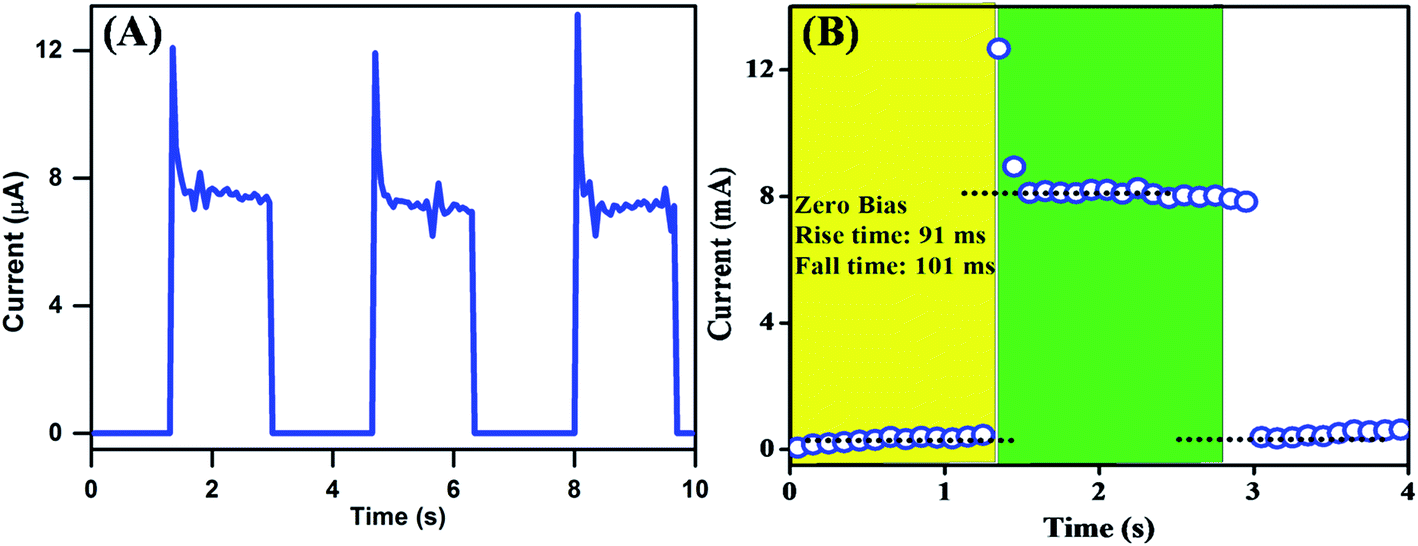 | ||
| Fig. 2 (A) The photodynamic response of the ITO/perovskite photodetector at zero bias under illumination of red light. (B) Magnified view of the non-saturated and saturated responses of the fabricated ITO/perovskite photodetector. | ||
A non-saturated response of a UV detector has been observed by others.43 They concluded the non-saturated response to be due to the large surface area of nanostructures and the presence of active surface defects, with these defects involved in multi-level charge transitions and resulting in a slowing down of the recombination process. However, the saturated photocurrent represented a combination of charge carrier transitions and defect levels.44,45 IL attained 90% of its maximum value within 91 ms, while in the absence of illumination no charge carriers were generated and decay in IL towards Id takes place with a decay time of 100 ms. The fabricated heterostructure exhibited a photosensitivity (IL − Id/Id) of 1.33 × 10². The obtained photodiode characteristics for the ITO/perovskite diode were found to be comparable to those reported for SnO2- and ZnO-based p–n junction photodiodes.1–3,33 The quantum efficiency describes the efficiency of the electron–hole pair generation and charge collection and is defined as 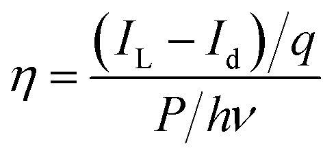 where q is the electron charge, hν is the photoenergy, and P is the incident power.7 A quantum efficiency value of 0.16 and spectral responsivity of 59.8 mA W−1 were obtained for the fabricated photodiode. In general, the current gain should be low for an efficient photodiode. The origin of the high photocurrent in the fabricated photodiode is discussed above in the context of Fig. 1C.
A schematic diagram of the as-prepared structure is shown in Fig. 3A. The observed photodynamic and Schottky behaviours can be further elucidated by the energy band diagrams corresponding to dark and illumination conditions. According to the developed working principle, a Schottky barrier was formed between the ITO glass and the perovskite as shown in Fig. 3B. The transfer of charge carriers between the ITO glass and CH3NH3Pbl3 occurred via Fermi level tuning, which can also lead to the accumulation of the charge carriers in the vicinity of the contact region, and depletion and space charge formation and band bending to form a Schottky barrier.31–33 The formation of depletion and the space charge region assisted the charge separation under illumination conditions. The photons having hv > Eg (semiconductor) can overcome the equilibrium state to form a Schottky barrier and generate a large number of electron–hole pairs (hv > e + h). The energy levels under dark and illumination conditions are illustrated in Fig. 3C and D. The electric field induced at the space charge region further and efficiently separated the photogenerated electrons from holes and thereby reduced the electron–hole recombination rate that can lead to an increase in the free charge carrier density.9,17–19 Upon illumination, the excess generated electron–hole pairs in CH3NH3Pbl3 changed the Fermi level in a way that can efficiently lower the effective barrier height and cause significantly easier transport and tunnelling.21,22
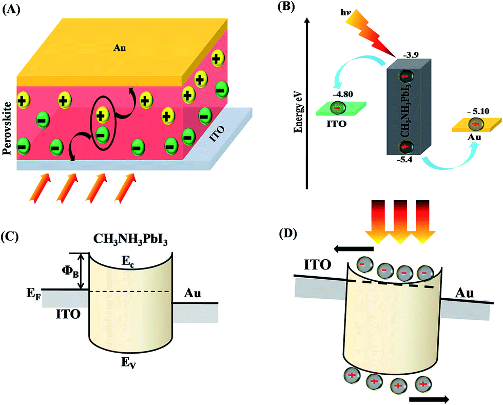 | ||
| Fig. 3 (A) Schematic diagram and the working principle of the photodetector. (B) Charge carrier transfer in the ITO/perovskite photodetector under illumination. (C, D) Schematic illustrations of energy levels of the ITO/perovskite photodetector (C) in the dark and (D) under illumination. | ||
The above discussion improves our understanding of photogenerated charge carrier separation and transport. The presented study also demonstrated efficient charge transport in CH3NH3Pbl3 semiconductor materials where photogenerated electrons were injected into the ITO contact while the holes were injected into the gold contact. The situation changed when illumination was turned off; here, the carrier recombination and effective barrier height increased due to a greatly reduced carrier density, resulting in a lower current as depicted in Fig. 3.
Conclusions
In conclusion, self-powered high-speed perovskite Schottky junction photodiodes were fabricated by using a low-cost solution processing method. The present report successfully demonstrated the in-depth detailed working mechanism of perovskite-based photodetectors as a function of bias and light by using net terminal current–voltage characteristics and photodynamic measurements. The work also illustrated the capability of the perovskite layer to generate and conduct both electron and hole carriers under illumination. The perovskite Schottky junction diode yielded a rectification behaviour with a low value of reverse saturation current under dark conditions, and a zero bias photocurrent under illumination. The fabricated photodiode exhibited high photosensitivity with fast response and recovery times. The demonstrated excellent performance and detailed working mechanism provide a way to fabricate an efficient self-bias photodiode for future electronic devices.References
- M. A. Green, A. Ho-Baillie and H. J. Snaith, Nat. Photonics, 2014, 8, 506–514 CrossRef CAS.
- P. Gao, M. Gratzel and M. K. Nazeeruddin, Energy Environ. Sci., 2014, 7, 2448–2463 CAS.
- M. M. Lee, J. Teuscher, T. Miyasaka, T. N. Murakami and H. J. Snaith, Science, 2012, 338, 643–647 CrossRef CAS PubMed.
- L. Wang, J. Jie, Z. Shao, Q. Zhang, X. Zhang, Y. Wang, Z. Sun and S.-T. Lee, Adv. Funct. Mater., 2015, 25, 2910–2919 CrossRef CAS.
- F. Lin, S.-W. Chen, J. Meng, G. Tse, X.-W. Fu, F.-J. Xu, B. Shen, Z.-M. Liao and D.-P. Yu, Appl. Phys. Lett., 2014, 105, 073103 CrossRef.
- C. Soci, A. Zhang, B. Xiang, S. A. Dayeh, D. P. R. Aplin, J. Park, X. Y. Bao, Y. H. Lo and D. Wang, Nano Lett., 2007, 7, 1003–1009 CrossRef CAS PubMed.
- P. Kumar, N. Saxena, S. Dewan, F. Singh and V. Gupta, Giant UV-sensitivity of ion beam irradiated nanocrystalline CdS thin films, RSC Adv., 2016, 6(5), 3642–3649 RSC.
- K. Das, S. Mukherjee, S. Manna, S. K. Ray and A. K. Raychaudhuri, Nanoscale, 2014, 6, 11232–11239 RSC.
- Q. Hong, Y. Cao, J. Xu, H. Lu, J. He and J.-L. Sun, ACS Appl. Mater. Interfaces, 2014, 6, 20887–20894 CAS.
- K. Domanski, W. Tress, T. Moehl, M. Saliba, M. K. Nazeeruddin and M. Grätzel, Adv. Funct. Mater., 2015, 25, 6936–6947 CrossRef CAS.
- J. Burschka, N. Pellet, S. J. Moon, R. Humphry-Baker, P. Gao, M. K. Nazeeruddin and M. Gratzel, Nature, 2013, 499, 316–319 CrossRef CAS PubMed.
- Y. Guo, C. Liu, H. Tanaka and E. Nakamura, J. Phys. Chem. Lett., 2015, 6, 535–539 CrossRef CAS PubMed.
- Y. Lee, J. Kwon, E. Hwang, C.-H. Ra, W. J. Yoo, J.-H. Ahn, J. H. Park and J. H. Cho, Adv. Mater., 2015, 27, 41–46 CrossRef CAS PubMed.
- Q. Lin, A. Armin, D. M. Lyons, P. L. Burn and P. Meredith, Adv. Mater., 2015, 27, 2060–2064 CrossRef CAS PubMed.
- J. M. Frost, K. T. Butler, F. Brivio, C. H. Hendon, M. van Schilfgaarde and A. Walsh, Nano Lett., 2014, 14, 2584–2590 CrossRef CAS PubMed.
- T. Leijtens, S. D. Stranks, G. E. Eperon, R. Lindblad, E. M. J. Johansson, I. J. McPherson, H. Rensmo, J. M. Ball, M. M. Lee and H. J. Snaith, ACS Nano, 2014, 8, 7147–7155 CrossRef CAS PubMed.
- S. Yang, J. Gong and Y. Deng, J. Mater. Chem., 2012, 22, 13899–13902 RSC.
- J. Zhou, L. Lin, L. Zhang and Z. Lin, J. Phys. Chem. C, 2011, 115, 16828–16832 CAS.
- X. Y. Chin, D. Cortecchia, J. Yin, A. Bruno and C. Soci, Nat. Commun., 2015, 6, 7383–7392 CrossRef CAS PubMed.
- Y. Zhang, R. Tao, X. Zhao, Z. Sun, Y. Wang and L. Xu, Chem. Commun., 2016, 52, 3304–3307 RSC.
- L. Dou, Y. Yang, J. You, Z. Hong, W.-H. Chang, G. Li and Y. Yang, Nat. Commun., 2014, 5, 5404–5410 CrossRef CAS PubMed.
- F. Wang, J. Mei, Y. Wang, L. Zhang, H. Zhao and D. Zhao, ACS Appl. Mater. Interfaces, 2016, 8, 2840–2846 CAS.
- J. Kim, S.-H. Lee, J. H. Lee and K.-H. Hong, J. Phys. Chem. Lett., 2014, 5, 1312–1317 CrossRef CAS PubMed.
- W.-J. Yin, T. Shi and Y. Yan, Appl. Phys. Lett., 2014, 104, 063903 CrossRef.
- X. Hu, X. Zhang, L. Liang, J. Bao, S. Li, W. Yang and Y. Xie, Adv. Funct. Mater., 2014, 24, 7373–7380 CrossRef CAS.
- R. Dong, Y. Fang, J. Chae, J. Dai, Z. Xiao, Q. Dong, Y. Yuan, A. Centrone, X. C. Zeng and J. Huang, Adv. Mater., 2015, 27, 1912–1918 CrossRef CAS PubMed.
- B. Murali, M. I. Saidaminov, A. L. Abdelhady, W. Peng, J. Liu, J. Pan, O. M. Bakr and O. F. Mohammed, J. Mater. Chem. C, 2016, 4, 2545–2552 RSC.
- D. Liu and T. L. Kelly, Nat. Photonics, 2014, 8, 133–138 CrossRef CAS.
- E. J. Juarez-Perez, R. S. Sanchez, L. Badia, G. Garcia-Belmonte, Y. S. Kang, I. Mora-Sero and J. Bisquert, J. Phys. Chem. Lett., 2014, 5, 2390–2394 CrossRef CAS PubMed.
- A. Mei, X. Li, L. Liu, Z. Ku, T. Liu, Y. Rong, M. Xu, M. Hu, J. Chen, Y. Yang, M. Grätzel and H. Han, Science, 2014, 345, 295–298 CrossRef CAS PubMed.
- B. Tripathi, P. Bhatt, P. Chandra Kanth, P. Yadav, B. Desai, M. Kumar Pandey and M. Kumar, Sol. Energy Mater. Sol. Cells, 2015, 132, 615–622 CrossRef CAS.
- P. Bhatt, K. Pandey, P. Yadav, B. Tripathi, P. Chandra kanth, M. K. Pandey and M. Kumar, Sol. Energy Mater. Sol. Cells, 2015, 140, 320–327 CrossRef CAS.
- P. Yadav, K. Pandey, P. Bhatt, D. Raval, B. Tripathi, C. P. Kanth, M. K. Pandey and M. Kumar, Sol. Energy, 2015, 122, 773–782 CrossRef CAS.
- H. T. Hsueh, S. J. Chang, W. Y. Weng, C. L. Hsu, T. J. Hsueh, F. Y. Hung, S. L. Wu and B. T. Dai, IEEE Trans. Nanotechnol., 2012, 11, 127–133 CrossRef.
- D. Y. Kim, J. Ryu, J. Manders, J. Lee and F. So, ACS Appl. Mater. Interfaces, 2014, 6, 1370–1374 CAS.
- M. Tyagi, M. Tomar and V. Gupta, Mater. Res. Bull., 2015, 66, 123–131 CrossRef CAS.
- K. Jiao, D. Zhang and Y. Chen, RSC Adv., 2014, 4, 55300–55304 RSC.
- P. Yadav, K. Pandey, B. Tripathi, C. M. Kumar, S. K. Srivastava, P. K. Singh and M. Kumar, Sol. Energy, 2015, 122, 1–10 CrossRef CAS.
- J. E. Garland, D. J. Crain and D. Roy, Sol. Energy, 2011, 85, 2912–2923 CrossRef CAS.
- N. Zeiri, S. Abdi-Ben Nasrallah, N. Sfina and M. Said, Infrared Phys. Technol., 2014, 64, 33–39 CAS.
- R. Peng, S. Jiao, H. Li and L. Zhao, J. Alloys Compd., 2015, 632, 575–579 CrossRef CAS.
- C. R. Gobbiner, A. V. M. Ali and D. Kekuda, J. Mater. Sci.: Mater. Electron., 2015, 26, 9801–9807 CrossRef CAS.
- D. Shao, M. Yu, H. Sun, T. Hu, J. lian and S. Sawyer, Nanoscale, 2013, 5, 3664–3667 RSC.
- M. Tyagi, M. Tomar and V. Gupta, J. Mater. Chem. C, 2014, 2, 2387–2393 RSC.
- H. K. Yadav, K. Sreenivas and V. Gupta, Appl. Phys. Lett., 2007, 90, 172113 CrossRef.
Footnote |
| † Electronic supplementary information (ESI) available. See DOI: 10.1039/c6ra18453g |
| This journal is © The Royal Society of Chemistry 2016 |