DOI:
10.1039/C6RA08679A
(Paper)
RSC Adv., 2016,
6, 72975-72984
An atomically thick titanium phosphate thin layer with enhancing electrochemical sensitivity toward Pb(II)
Received
5th April 2016
, Accepted 21st July 2016
First published on 22nd July 2016
Abstract
Here we show for the first time the stripping signals for sensitivity identification of Pb(II) using a titanium phosphate (TiP) thin layer. An atomically thick TiP thin layer with 0.70 nm has been successfully exfoliated from the bulk α-TiP. A sensing interface for ultra-sensitive detection of Pb(II) by using the TiP thin layer as an electrode coating has been demonstrated for ultra-sensitive and selective electrochemical sensing toward heavy metal ions (e.g., Pb(II)). A range of Pb(II) contents in micro-moles (0.05 to 0.6 μM) at the TiP thin layer with a sensitivity of 23.60 μA μM−1 and a limit of detection of 0.91 nM have been investigated. Determining the responses of Zn(II), Cd(II), Cu(II) and Hg(II) as the most appropriate choice for comparison, the stripping voltammetric quantification of Pb(II) with high sensitivity and selectivity at the thin layer has been proved. As compared with bulk α-TiP, the TiP thin layer exhibited better detection performance toward Pb(II) which could be ascribed to the atomic thickness and higher adsorption capacity. Furthermore, XPS was applied to characterize the sorption behavior of Pb(II) on the surface of the TiP thin layer. Importantly, this work has a wider significance in that the system of an atomically thin layer offers possibilities to improve the sensitivity of the electrochemical analysis for Pb(II).
Introduction
As is known, a serious threat to public health will be caused by heavy metal ion (HMIs) contamination in drinking water even at a very low concentration.1–3 Specifically, Pb(II) has been recognized as a notorious heavy metal ion among all of the HMIs. Considering its ubiquitous presence in wastewater can cause many adverse effects on organisms e.g. the human nervous system, kidneys, blood circulation system, and so on,4,5 the World Health Organization (WHO) provisional guideline value is below 48.31 nM in drinking water. Therefore, sufficient concern on the environmental dangers of Pb(II) pollution and remarkable efforts towards developing analytical methods are necessary. Up to now, a variety of analytical methods have been applied to detect Pb(II), but electrochemical method has been recognized as an efficient method in detection of Pb(II) due to its fast detection speed, favorable stability, easiness to use and low cost.3,6–9 However, one of the great challenges is how to improve the sensitivity of sensing Pb(II) with electrochemical methods.
As reported in the literature, various composite modified electrodes have been employed to measure Pb(II).10–14 Otherwise, it has been demonstrated that the selective adsorption properties of the materials should be responsible for their highly beneficial for electrochemical detection.13,15,16 The metal phosphate nanomaterials including zirconium phosphate (ZrP), tin(IV) phosphates and titanium phosphate (TiP) and their compound have shown excellent adsorption capacity toward heavy metal ions and well selective adsorption toward Pb(II).17–23 In spite that some properties of these materials e.g. intercalation chemistry, catalytic properties, ion exchange capacities have been widely investigated,18,24–27 however, to our best knowledge, the electrochemical applications of metal phosphate materials have been done little which may be due to the poor conductive properties. As reported, after the exfoliation of layered compounds, the active functional groups, reactivity of the material and electrochemical activities can efficiently improved.28–30 A progress have been made by our group on electrochemical determination of Pb(II) based on exfoliated ZrP thin layer coating on the electrode surface.31 It is verified that the ZrP thin layer showed the strongest adsorption capability toward Pb(II) among all heavy metal ions, thereby resulting in selective detection consequently.
In this work, using the same method based on previous study,31 amorphous phase formation of atomically thick TiP thin layer was prepared via a simple hydrothermal process and intercalation reaction subsequently. Applied TiP thin layer as sensing materials for the analysis of Pb(II) with square wave anodic stripping voltammetry (SWASV), we show firstly that the stripping signals for selective detection of Pb(II). Firstly, the synthesized TiP thin layer was investigated by TEM (Transmission Electron Microscopy), XRD (X-ray diffraction), and EDS (Energy Dispersive Spectroscopy). Next, Pb(II) detection was studied by SWASV. The SWASV signal had higher sensitivity than commonly used electrodes. To gain further insight into sorption mechanism, XPS analysis of TiP thin layer before and after Pb(II) ion loading were performed, showing that Pb(II) loaded on TiP thin layer depends mainly on the formation of the inner sphere complex with TiP by Ti–O–Pb. In addition, the possibility of the use of TiP thin layer for electrochemical analysis of Pb(II) is greatly important for ultra-trace detection of Pb(II) in real samples. The application of atomically thin layer will offer the possibilities to realize the improved sensitivity in electrochemical analysis.
Experimental
Reagents and sample
Tetra-tert-butyl orthotitanate (Ti(OC4H9)4), phosphoric acid (85%), Pb(NO3)2, 3CdSO4·8H2O, Cu(NO3)2, Hg(NO3)2, Zn(NO3)2, and 25 wt% tetramethylammonium hydroxide (TMA+OH−) solution were purchased from Sinopharm Chemical Reagent Co., Ltd. (China). All chemicals used were analytical grade and were used as received without any further purification. Acetate buffer solutions of 0.1 M for different pH were prepared by mixing stock solutions of 0.1 M HAc and NaAc. All solutions were prepared with deionized water of resistivity not less than 18.2 MΩ cm.
Apparatus
Electrochemical experiments were performed with a CHI 660D computer-controlled potentiostat (ChenHua Instruments Co., Shanghai, China) with a standard three electrode system. A bare glassy carbon electrode (GCE, diameter of 3 mm) or modified GCE served as a working electrode; a platinum wire was used as a counter-electrode with a saturated Ag/AgCl electrode (ChenHua Instruments Co., Shanghai, China) completing the cell assembly. Transmission electron microscopy (TEM) and energy-dispersive spectrometer (EDS) were recorded using a JEM-2010 transmission electron microscope operated at 200 KV (Quantitative method: Cliff Lorimer thin ratio section). X-ray diffraction (XRD) patterns were recorded in the range of 2θ = 10–40° with a Philips X'Pert X-ray diffractometer, using Cu Kα (λKα1 = 1.5418 Å) as the radiation source. Atomic force microscopy (AFM) images were carried out using Nanoscope III (Digital Instruments, Veeco Metrology). pH value was measured using pH meter (Model: PHS-3C). Deionized (DI) water (18.2 MΩ cm) was used to prepare all solutions and was purified with the NANO pure Diamond UV water system. All experiments were carried out at 295 ± 3 K.
Real sample preparation
Bulk α-TiP was prepared according to previous report with minor modification.21 In brief, 8.5 g Ti(OC4H9)4 was mixed with 9.8 g of H3PO4 (85 wt%) in Teflon-lined stainless steel autoclave and heated at 150 °C in an electric oven for 24 h, After cooling to room temperature naturally, the product was washed by water and collected by centrifugation some times. Then, the solid was dried at 85 °C for 24 h under vacuum. The dried Ti(HPO4)2 was ground using a mortar and pestle into powder. The precursor bulk α-TiP was exfoliated in an aqueous dispersion solution containing 25 wt% TMA+OH− under stirring at room temperature for 7 h.32 Then the products were washed and collected by centrifugation and dried at 65 °C with vacuum.
Electrode fabrication
Prior to modification, GCE was polished with 1.0, 0.3 and 0.05 μm of alumina power and then successively sonicated with 1![[thin space (1/6-em)]](https://www.rsc.org/images/entities/char_2009.gif) :1 HNO3, alcohol and ultrapure water, respectively. The construction of TiP thin layer on the surface of GCE was performed as follows: 5 mg of TiP thin layer was suspended in 1 mL of distilled water to form a suspension. The suspension was then briefly sonicated for 30 s in order to disperse the nanocomposites. Then, a 4 μL aliquot of this suspension was then pipetted onto the surface of a freshly polished GCE and evaporated at room temperature. Similar procedure was used to prepare bulk α-TiP modified electrode.
:1 HNO3, alcohol and ultrapure water, respectively. The construction of TiP thin layer on the surface of GCE was performed as follows: 5 mg of TiP thin layer was suspended in 1 mL of distilled water to form a suspension. The suspension was then briefly sonicated for 30 s in order to disperse the nanocomposites. Then, a 4 μL aliquot of this suspension was then pipetted onto the surface of a freshly polished GCE and evaporated at room temperature. Similar procedure was used to prepare bulk α-TiP modified electrode.
Electrochemical experiments
Square wave anodic stripping voltammetry was used for Pb(II) detection under optimized conditions. The as-prepared TiP thin layer GCE was dipped in a stirred analyte solution of 0.1 M NaAc–HAc (pH 4.0) containing Pb(II) and kept at −1.1 V for 120 s. The anodic stripping (reoxidation of metal to metal ions) of electrodeposited metal was performed in the potential range of −1.0 to −0.2 V with step potential of 4 mV, amplitude of 25 mV, and frequency of 15 Hz. A desorption potential of 0 V for 150 s was performed to remove the residual metals under stirring condition. The individual detection of Zn(II), Cd(II), Cu(II), and Hg(II) has been operated at the same experimental conditions (except Zn(II) with a deposition potential of −1.3 V for 120 s. This is because only when deposition potential is more negative (100–300 mV) than the potential for stripping peak, metal ions could be deposited on the electrode surface in the deposition step. Generally, the stripping peak for Zn(II) emerges at around −1.1 V.). For comparison, other modified electrodes were used the same process and conditions. All experiments were performed at room temperature under air atmosphere.
Results and discussion
Detection strategy of Pb
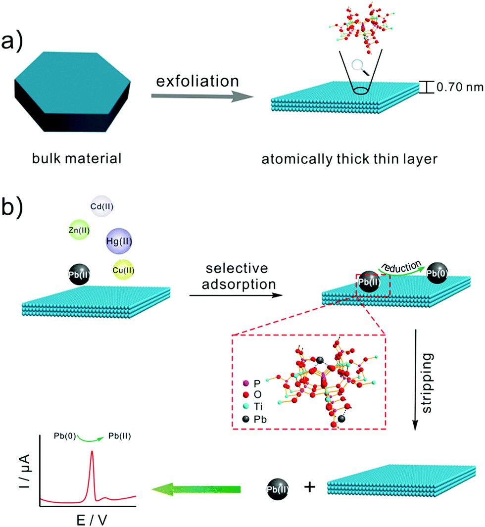
Scheme 1 illustrates (a) the synthesis of TiP thin layer and (b) selective electrochemical detection of Pb(II). Bulk α-TiP has a layered structure in which the metal atoms lie nearly in a plane and layers are formed by titanium atoms connected through the oxygen atoms of the phosphate groups. Each phosphate contributes three of its oxygen atoms to the formation of these layers, leaving one –OH group pointing into the interlayer space. This structure gives α-TiP a much higher ion exchange capacity.33 Exchange occurs by replacement of the orthophosphate hydrogen by cations which then occupy positions between the interlayer region.34 As shown in Scheme 1, following by the addition of TMA+, the interlayer space will be large enough to form fully exfoliated TiP thin layer nano-composites. After the exfoliation, TiP thin layer expose more –OH which is benefit to the adsorption of Pb(II). The Pb(II) ions may be adsorbed on the thin layer TiP at two different types of exposed oxygen atoms: the oxygen atoms bridging the Ti and P atoms and those in the hydroxyl groups linked to the P atoms (termed as terminal oxygens) as shown in Scheme 1. Then the metal ions adsorbed on TiP surface are identified by square wave anodic stripping voltammetry technique. The adsorbed Pb(II) by TiP thin layer will be reduced to Pb(0) holding at a certain potential, and the reoxidation of Pb(0) will give the anodic stripping current which associated with the amount of Pb(II) on electrode surface. Compared with the other commonly heavy metal ions (e.g., Zn(II), Cd(II), Cu(II), and Hg(II)), Pb(II) was suggested to have the largest binding affinity resulting in the highest adsorbing capacity on surface of TiP thin layer.
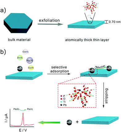 |
| | Scheme 1 Schematic illustration of (a) the synthesis of TiP thin layer and (b) selective electrochemical detection of Pb(II). | |
Morphology and composition characterization
Fig. 1a shows the representative transmission electron microscope (TEM) images of bulk α-TiP with a lateral dimension of ∼800 nm and a vertical length of ∼1 μm. The TiP thin layer displayed in Fig. 1b has much small size and different morphology compared with bulk α-TiP. The thickness of the TiP thin layer is about 0.70 nm confirmed by atomic force microscopy (Fig. 1c and d) which is much thinner than bulk α-TiP indicating that the bulk α-TiP has been successfully exfoliated. Furthermore, the disappearance of the typical diffraction peaks at TiP thin layer compared with the primary diffraction of bulk α-TiP further revealed that the TiP thin layer is prepared (Fig. 1e). The smaller size and thinner thickness of TiP thin layer are both result from the destruction of α-TiP during the exfoliation.
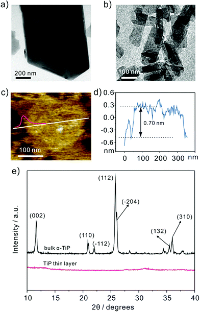 |
| | Fig. 1 Representative TEM images of (a) bulk α-TiP and (b) TiP thin layer. The (c) and (d) AFM image of TiP thin layer with height profile. (e) XRD patterns of bulk α-TiP and TiP thin layer. | |
In addition, as shown in Fig. 2, the P/Ti ratio in bulk α-TiP is characterized as approximately 2:1 by EDS analysis, which is consistent with its stoichiometry as Ti(HPO4)2. However, the ratio in TiP thin layer is found to be less than 2. It is suggested that during the exfoliation the hydrolysis occurs releasing a massive amount of P and negligible Ti into liquid phase because phosphate groups on the edges are accessible to base, resulting in the ratio of P/Ti below 2.35,36 Otherwise, the decrease of P and the high exposure of O atoms on TiP thin layer will result in the formation of –OH in aqueous solution and is benefit to the adsorption of Pb(II).
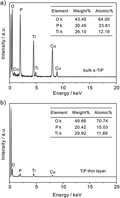 |
| | Fig. 2 EDS spectrum of (a) bulk α-TiP and (b) TiP thin layer. | |
Electrochemical characterization
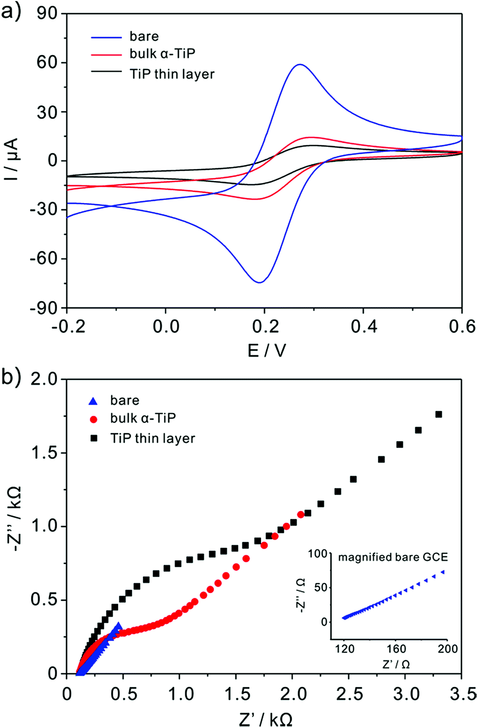
The nature of the modified electrodes and the influence of nanoparticles on electron-transfer kinetics are measured by cyclic voltammetry (CV) and impedance techniques. The typical CV of bare, bulk α-TiP and TiP thin layer modified GCE are characterized in 5 mM K3Fe(CN)6 containing 0.1 M KCl and the scanning rate is 0.1 V s−1 (Fig. 3a). As compared with bare GCE, the anodic and cathodic peak currents are decreased markedly at bulk α-TiP and TiP thin layer modified electrode indicating the poor conductivity of bulk α-TiP and TiP thin layer. The bulk α-TiP and TiP thin layer modified electrode also show poor electron-transfer kinetics for the Fe(CN)63−/4− redox couple revealing that the bulk α-TiP and TiP thin layer modified electrode hinder the electron-transfer process. Furthermore, TiP thin layer has more poor conductivity than bulk α-TiP due to the addition of organic ion.
 |
| | Fig. 3 Cyclic voltammograms (a) of bare (blue color line), bulk α-TiP (red color line) and TiP thin layer (black color line) modified GCE in the solution of 5 mM Fe(CN)63−/4− containing 0.1 M KCl and (b) the corresponding Nyquist diagram of electrochemical impedance spectra. Inset is the partial magnified EIS of bare GCE. | |
The interface properties of the bare, bulk α-TiP and TiP thin layer modified electrode are further estimated with electrochemical impedance resistance (EIS). EIS is an elegant method to probe the changes of electron transfer resistance on the electrode surface before and after being modified as shown in Fig. 3b. The sequence of EIS is TiP thin layer > bulk α-TiP > bare GCE, and the increased electron transfer resistance also demonstrates the poor conductivities of bulk α-TiP and TiP thin layer.
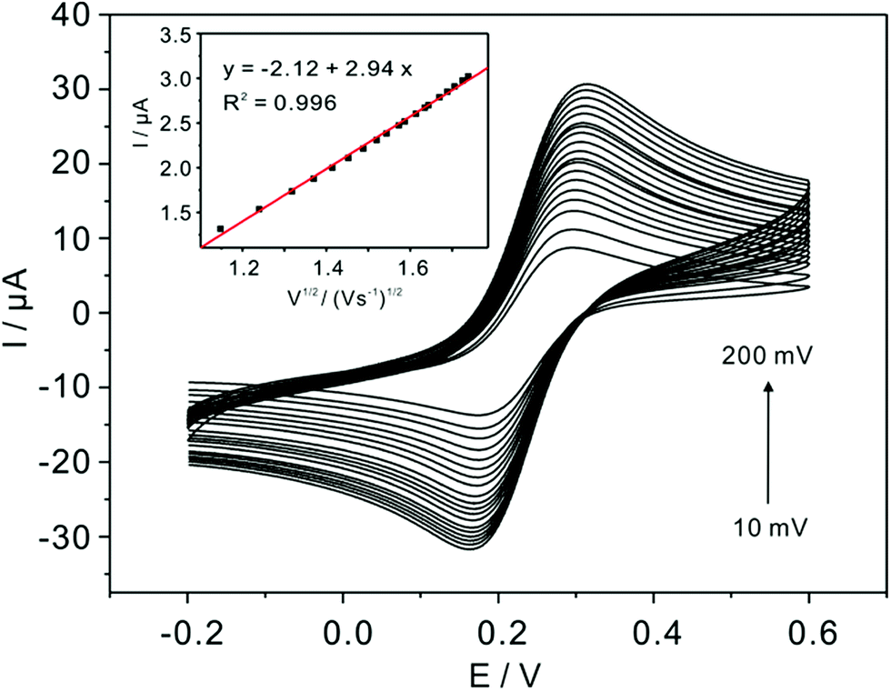
The real electrochemical surface areas (ECSAs) are characterized by cyclic voltammetric in 5 mM Fe(CN)63−/4− containing 0.1 M KCl at various scan rates shown in Fig. 4. According to the Randles–Sevcik equation, ip = (2.69 × 10⁵)n3/2ACD1/2v1/2, the ECSAs of the bare, bulk α-TiP and TiP thin layer modified are calculated to be 0.07, 0.0081 and 0.00085 cm2, respectively. This result confirms that the introduction of bulk α-TiP and TiP thin layer could greatly reduce the electrochemical active electrode surface.
 |
| | Fig. 4 Scan rate study (from 0.01 to 0.2 V s−1) in the solution of 5 mM Fe(CN)63−/4− containing 0.1 M KCl at TiP thin layer modified GCE. Inset is the corresponding plots of current versus the square root of the scan rate with a linear trend line. | |
Optimization of the stripping parameters
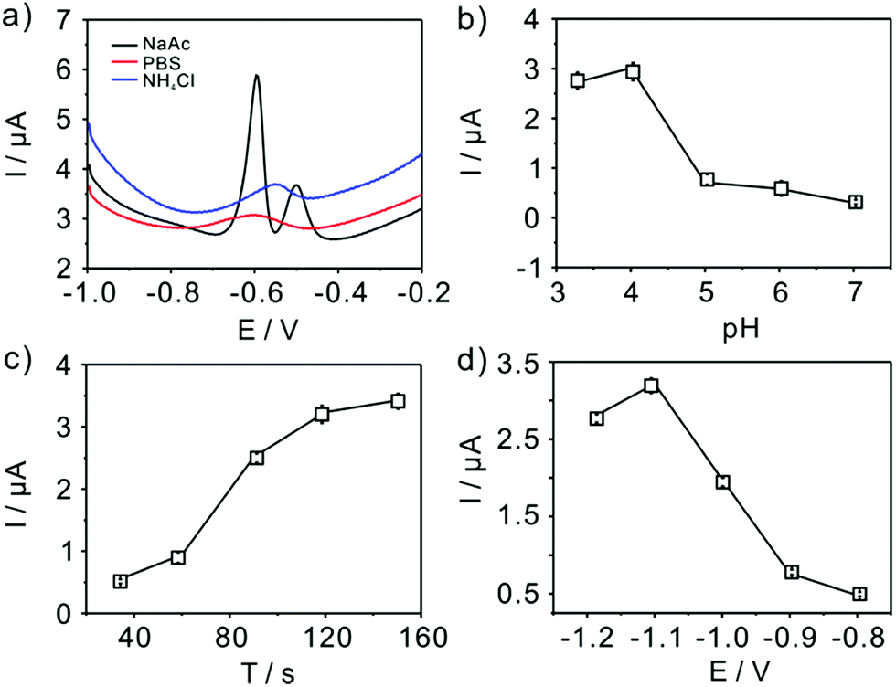
The experimental conditions, such as supporting electrolytes, pH, deposition potential and deposition time, are firstly studied to get maximum sensitivity for Pb(II) detection with TiP thin layer modified GCE shown in Fig. 5. The effect of supporting electrolytes (pH 4.0) is tested and acetate buffer solutions are finally selected as the best electrolyte compared with phosphate buffer solution (PBS) and NH4Cl–HCl (Fig. 5a). As shown in Fig. 5, a double stripping peak for electroanalysis of Pb(II) is clearly seen at TiP thin layer modified GCE, where one peak appears at around −0.62 V and the other is around −0.51 V. The well-known Pb/Pb2+ couple stripping peaks have been observed in many works31,37,38 and have attributed loosely to the “nature” of the metal deposit on the surface. Hutton et al.38 proposed a new insights into the deposition and stripping process through the use of AFM. They attributed this phenomenon to the difference among the morphologies of deposited lead on the electrode surface in various concentration regime. In this work, two peaks are emerged in Fig. 5a in NaAc solution. It is believed that in NaAc solution Pb(II) would be more easier to deposited on the surface of electrode forming a “grain-independent heterogeneous structures”. However, much more studies are necessary to clarify this. The effect of pH (from 3.0 to 7.0) on the stripping peak current is summarized in Fig. 5b. Clearly, the maximum stripping peak current is achieved when the solution is maintained at pH 4.0. Therefore, pH 4.0 in 0.1 M acetate buffer solution is chose for all subsequent electrochemical detection. Fig. 5c shows the change of the stripping peak current with the pre-concentration time (from 30 s to 150 s). As shown in Fig. 5c, the stripping current increases linearly with the increase of the deposition time up to 120 s. However, the current increase reached a nearly plateau when further increasing the deposition time. The dynamic equilibrium for Pb(II) adsorption and/or deposition could be responsible for this phenomenon. Taking both the sensitivity and efficiency into account, a deposition time of 120 s is employed in the experiments. The application of adequate deposition potential is very important to obtain the best sensitivity. Thus, the effect of the deposition potential on the peak current after 120 s deposition is investigated in the potential range from −1.2 V to −0.8 V. As shown clearly (Fig. 5d), the peak current for Pb(II) increases as the deposition potential is changed from −1.2 V to −1.1 V, reaching a maximum at −1.1 V, and then decreases with further increased deposition potential up to −0.8 V. Therefore, we choose −1.1 V as deposition potential for further detection of Pb(II). In a word, all the electrochemical below is executed in 0.1 M pH 4 acetate buffer and a deposition potential of −1.1 V with 120 s.
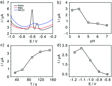 |
| | Fig. 5 Optimal experimental conditions. Influence of (a) supporting electrolytes; (b) pH value; (c) accumulation time; and (d) deposition potential on the voltammetric response of TiP thin layer modified GCE. Data are extracted from SWASV of 0.2 μM Pb(II). | |
Detection of heavy metal ions
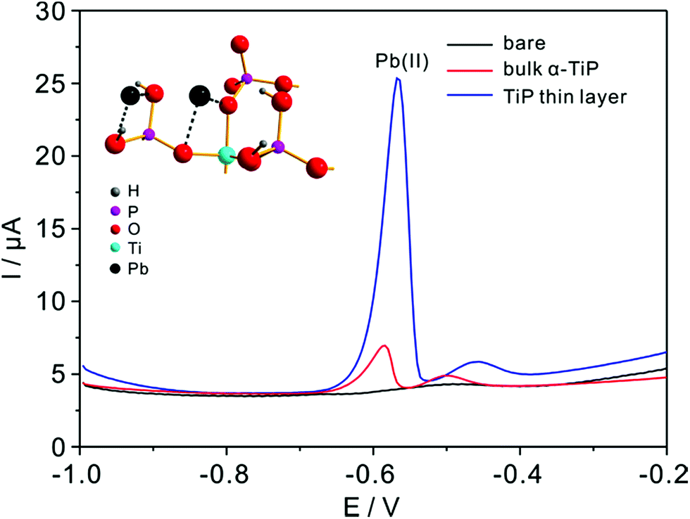
Detection experiments toward Pb(II) on modified electrodes are first examined by SWASV in NaAc–HAc solution in the presence of 0.8 μM Pb(II) (Fig. 6). The voltammetric stripping peak at −0.58 V for Pb(II) detection are observed on the surface of bulk α-TiP and TiP thin layer modified GCE. The sharp peak corresponds to the oxidation of Pb(0) to Pb(II) on bulk α-TiP and TiP thin layer modified GCE while no signal on bare GCE. The highest response of TiP thin layer indicate that the modification of TiP thin layer will greatly enhance the Pb(II) adsorption ability and the enhanced reactivity.
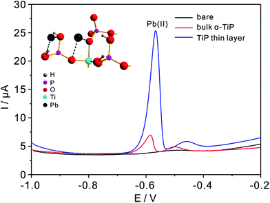 |
| | Fig. 6 Typical SWASV responses of 0.8 μM Pb(II) at bare (black line), bulk α-TiP (red line), and TiP thin layer modified (blue line) GCE in 0.1 M NaAc–HAc solution (pH 4.0). The inset is the magnified structure with adsorbed Pb ions on oxygen atoms (some coordinated oxygen atoms of P and Ti atoms are omitted for clarify). | |
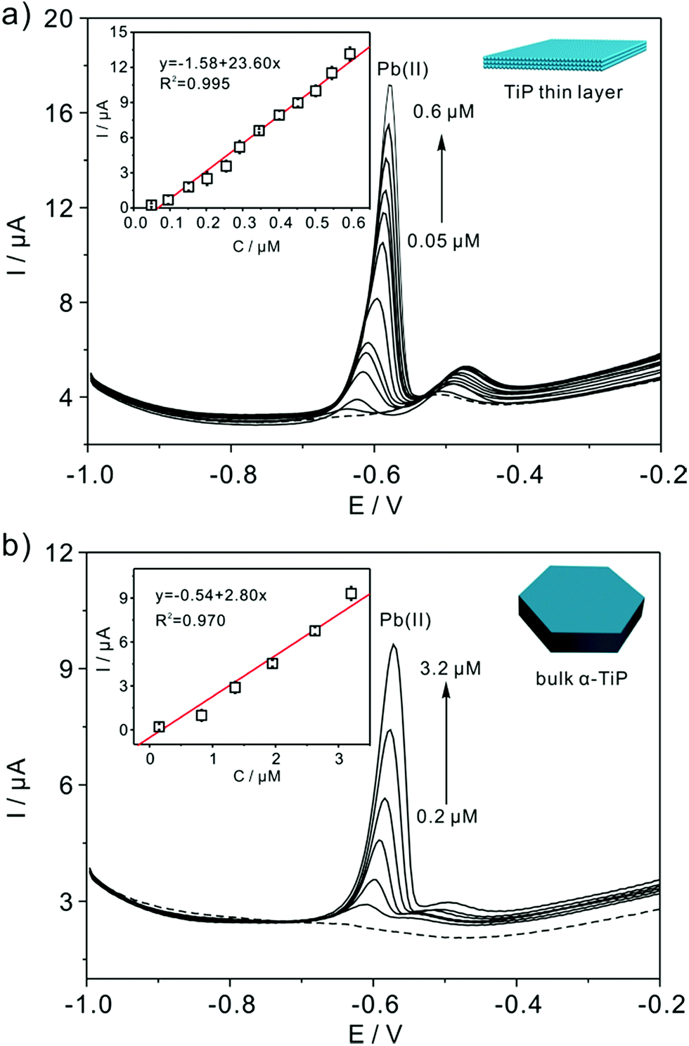
Fig. 7a shows the SWASV responses of the TiP thin layer modified GCE toward Pb(II) at a range of concentrations under optimal conditions. As shown in Fig. 7a, the stripping peak current (i) is proportional to the concentration of Pb(II) in the range of 0.05–0.6 μM. The linearization equation is ip (μA) = 1.58 + 23.60c (μM), with the correlation coefficients of 0.995. A high sensitivity of 23.60 μA μM−1 Pb(II) is achieved with the limit of detection (LOD) as low as 0.91 nM using 3σ method (3σ method, the 3σ LOD is calculated from 3SD/S, where SD is the standard deviation of the measurements and S is the slope of the calibration graph). The LOD is far below the requirements of the World Health Organization (WHO) maximum permissible limit for Pb concentration in drinking water. As shown in Table 1, the sensitivity and LOD of TiP thin layer are both impressive compared with some other electrodes. For comparison, the response of bulk α-TiP modified GCE toward Pb(II) is also studied with a sensitivity of 2.80 μA μM−1 shown in Fig. 7b. In contrast to TiP thin layer, the response at bulk α-TiP modified electrode is about 8 fold lower than that of TiP thin layer. The better performance of TiP thin layer could be ascribed to the higher adsorptivity toward Pb(II); this is consistent with our previous research.31,39 Otherwise, the TiP thin layer has a thinner thickness which possibly facilitate to the spread of the Pb(II) between the electrode and TiP surface. The outstanding performance of ultrathin materials with atomic thickness is confirmed.
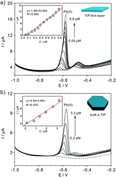 |
| | Fig. 7 Typical SWASV stripping signals of Pb(II) at TiP thin layer (a) and (b) bulk α-TiP modified GCE. The insets are the calibration plot of the SWASV peak current versus the concentration of Pb(II), respectively. | |
Table 1 Comparison of current sensitivity with previously reported values on different modified electrodes
| Electrodes |
Electrolyte |
Sensitivity (μA μM−1) |
LOD (μM) |
Ref. |
| Au nanoparticles/GCE |
0.1 M NaAc–HAc (pH 5.0) |
17.63 |
0.3 |
40 |
| Poly(ρ-PD) modified carbon paste electrode |
0.1 M KNO3 (pH 12.0) |
2.71 |
0.001 |
41 |
| TPP-kaolinite modified carbon paste electrode |
0.1 M NaAc–HAc (pH 4.5) |
0.910 × 10⁻⁶ |
0.084 |
42 |
| Z-BHPBP/MWCNT modified carbon paste electrode |
B–R buffer solution (pH 3.5) |
15.67 |
1.20 |
43 |
| Nano-zirconium phosphate/GCE |
0.1 M NaAc–HAc (pH 4.0) |
31.54 |
1.9 × 10⁻⁵ |
31 |
| Polycrystalline boron doped diamond electrode |
0.1 M KNO3 |
— |
4 × 10⁻³ |
38 |
| Hg-free carbon fiber microelectrode |
Tris-buffer ingredients |
1.7 × 10⁻⁴ |
8.4 |
44 |
| Carbon paste electrode |
0.1 M HAc–NaAc (pH 4.0) |
7.59 |
1 × 10⁻⁴ |
45 |
| NiCo2O4/GCE |
0.1 M NaAc–HAc (pH 5.0) |
26.97 |
0.089 |
46 |
| Graphite electrode |
0.1 M HCl |
— |
10−3 |
47 |
| Bi/GCE |
0.1 M HAc–NaAc (pH 4.5) |
4.78 |
5.31 × 10⁻³ |
48 |
| Gold nanofilm electrodes |
0.1 M PBS (pH 7.0) |
— |
0.1 |
49 |
| AlOOH-RGO/GCE |
0.1 M HAc–NaAc (pH 6.0) |
2.97 |
7.6 × 10⁻⁵ |
50 |
| Co3O4/Nafion/GCE |
0.1 M HAc–NaAc (pH 5.0) |
28.3 |
0.0520 |
51 |
| Nanoplate-stacked Fe3O4 modified electrode |
0.1 M HAc–NaAc (pH 5.0) |
24.6 |
0.0152 |
52 |
| Titanium phosphate thin layer/GCE |
0.1 M HAc–NaAc (pH 4.0) |
23.60 |
9.1 × 10⁻⁴ |
This work |
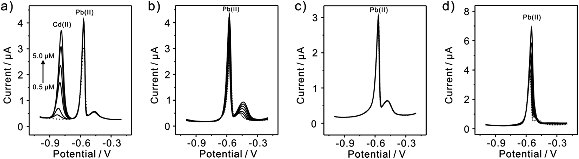
Subsequently, the electrochemical behaviors of TiP thin layer modified GCE for the detection of Cd(II), Cu(II), Hg(II), and Zn(II) are also explored under the same conditions (except Zn(II) deposited at −1.3 V). The typical SWASV stripping signals and the corresponding calibration plots of Cd(II), Cu(II), Hg(II), and Zn(II) at the TiP thin layer modified GCE are shown in detail in Fig. 8. The sensitivities and LODs of those heavy metal ions including Pb(II) on TiP thin layer GCE are systematically compared in Fig. 9. As shown, the achieved sensitivity toward Pb(II) on TiP thin layer GCE is around 7–8 times higher than that toward Cd(II), Cu(II) and Zn(II) and 14 times higher than that toward Hg(II). The outstanding adsorption ability of TiP thin layer toward Pb(II) which is much stronger than other heavy metal ions under the same accumulation conditions should be responsible for it.
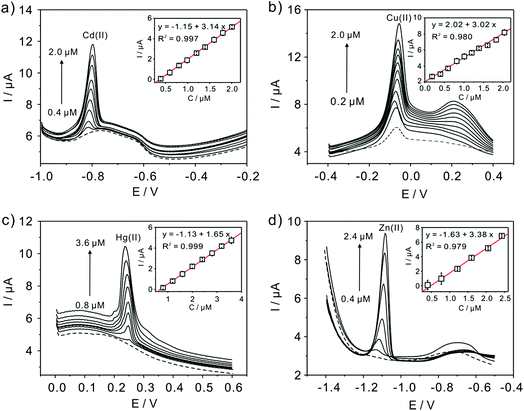 |
| | Fig. 8 Typical SWASV stripping signals of (a) Cd(II), (b) Cu(II), (c) Hg(II), and (d) Zn(II) at the TiP thin layer modified GCE, respectively. The insets are the corresponding calibration plots. | |
 |
| | Fig. 9 Sensitivities of metal ions at the TiP thin layer modified GCE in the presence of Pb(II), Cd(II), Hg(II), Zn(II) and Cu(II), respectively. Dates are collected from SWASV responses of Fig. 8. The insets are the comparation of LODs. | |
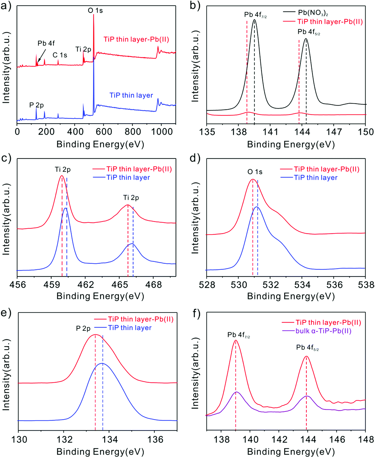
Peng et al. suggested that the hydroxyl groups in activated Ti sites will facilitate the sorption behavior to Pb(II) through experimental and computational studies.53 In our study, the main reasons are may be that the Pb(II) loaded on TiP thin layer depends mainly on the formation of the inner sphere complex with TiP by Ti–O–Pb,54 while uptake of other cations is only driven by electrostatic interaction. To gain further insight into sorption mechanism, XPS analysis of TiP thin layer before and after Pb(II) ion loading were performed. As shown in Fig. 10b, the Pb(II) binding energies of purified Pb(NO3)2 are at 144.5 eV for Pb 4f5/2 and 139.6 eV for Pb 4f7/2, respectively. After Pb(II) loaded TiP thin layer samples, a remarkable shift of 0.6 eV to lower binding energy of Pb 4f was observed. This shift indicates the formation of strong affinities between the Pb(II) ions and TiP thin layer. Similar shifts of 0.3 eV were also observed for the Ti 2p (Fig. 10c), O 1s (Fig. 10d) and P 2p (Fig. 10e), confirming the possible strong interaction between Ti–O and Pb(II) ions. For comparison, the Pb 4f spectra onto TiP thin layer and onto bulk α-TiP are also shown in Fig. 10f. The intensity of the peak onto TiP thin layer is stronger than adsorbed on bulk α-TiP, which indicates that the amount of adsorbed Pb(II) is the more on TiP thin layer surface, further improving the stripping behaviors.
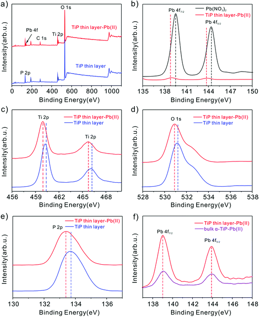 |
| | Fig. 10 (a) XPS spectra of TiP thin layer samples before and after adsorption of Pb(II) ions; (b) the Pb 4f spectra comparison of Pb(NO3)2 and that onto TiP thin layer samples; (c–e) the Ti 2p, O 1s and P 2p binding energy shifting before and after Pb(II) uptake; (f) the Pb 4f spectra comparison of Pb(II) onto TiP thin layer and onto bulk α-TiP samples. | |
Otherwise, the large surface areas of the laminate nanostructure produced by exfoliation and low hydration energy with divalent cation maybe also both result in the high selective sorption of Pb(II).53 It is suggested that the selective response of TiP thin layer originates from its highly selective adsorption. However, more works are ongoing in an attempt to clarify it, for instance, the comparison of different ions adsorption quantity, the combination of different ions and a comparison for relative bonding energies of different metal ions which the energetic data would be carried out.
Interference measurements
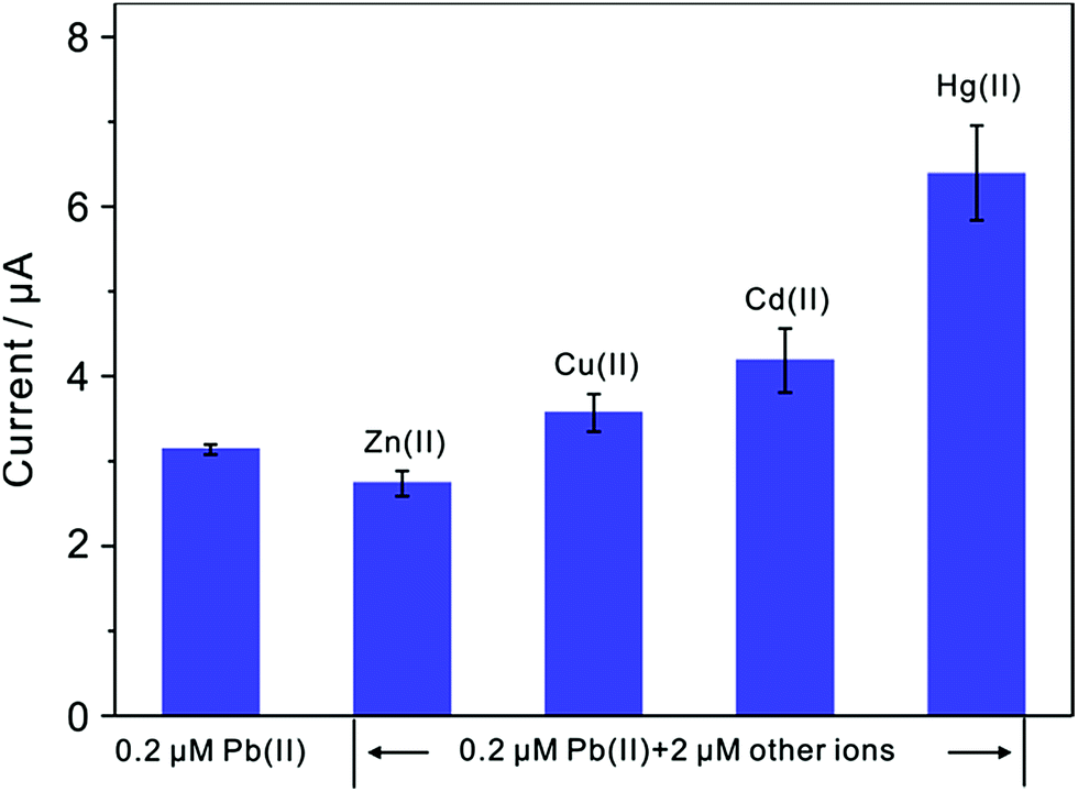
Since interference is a common problem in electrochemical detection, the interferences are also performed at TiP thin layer modified electrode under the optimal experimental conditions. Fig. 11 presents the SWASV responses toward 0.2 μM Pb(II) at TiP thin layer modified electrodes with the respective addition of various concentration of Cd(II), Cu(II), Zn(II), and Hg(II) in 0.1 M HAc–NaAc (pH 4.0), respectively. The interference results of Cd(II), Cu(II), Zn(II) and Hg(II) toward Pb(II) collected from SWASV responses are summarized in Fig. 12. It is clear that no significant change can be observed on TiP thin layer modified electrode though adding 2 μM Zn(II) and Cu(II) in which 0.2 μM Pb(II) is existed, respectively. This result indicates that Zn(II) and Cu(II) do not interference the adsorption toward Pb(II) on TiP thin layer. However, the peak current of Pb(II) become higher on TiP thin layer modified electrode when the concentration of Cd(II) (increased by 44%) and Hg(II) (increased by 111%) is increased to 10-fold concentration as Pb(II). The phenomenon is due to that Cd films and Hg films are formed on the electrodes.
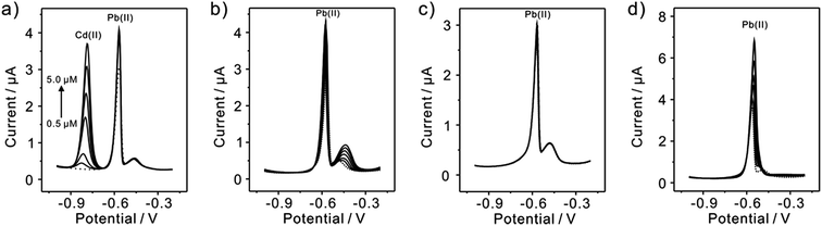 |
| | Fig. 11 Interference studies of typical SWASV responses of 0.2 μM Pb(II) on TiP thin layer modified electrodes in HAc–NaAc (pH 4.0) at different concentration of (a) Cd(II), (b) Cu(II), (c) Zn(II) and (d) Hg(II), respectively. Dotted lines represent the SWASV responses in the absence of Cd(II), Cu(II), Zn(II) and Hg(II), respectively. | |
 |
| | Fig. 12 Interference measurement of the TiP thin layer modified GCE in 0.1 M HAc–NaAc (pH 4.0) containing 0.2 μM Pb(II) in the presence of 2 μM Zn(II), Cu(II), Cd(II) and Hg(II), respectively. Dates are collected from SWASV responses of Fig. 11. Error bars correspond to standard errors measured from three independent measurements. | |
Analysis of Pb(II) in real water
For the practical application of the modified electrode, TiP thin layer modified GCE was used to detect Pb(II) in real sample which is collected from the Dongpu Reservoir in Hefei City, Anhui, China. The real sample was diluted with 0.1 M NaAc–HAc buffer solution (pH 4.0) in a ratio of 1:1 without further treatment. The recovery of Pb(II) was determined using the SWASV through standard additions of Pb(II) into the real samples demonstrating the practicality of TiP thin layer modified GCE (Table 2). The recovery was calculated to be 90–100% indicating that the modified electrode has a good practical application potential.
Table 2 Detection of spiked Pb(II) in real water at TiP thin layer modified GCE
| |
Concentrations of Pb(II) |
Recovery (%) |
RSD (%) |
| Added (μM) |
Found (μM) |
| Sample 1 |
0.20 |
0.195 |
97.5 |
1.37 |
| Sample 2 |
0.25 |
0.235 |
94.0 |
1.19 |
| Sample 3 |
0.30 |
0.288 |
96.0 |
0.98 |
| Sample 4 |
0.35 |
0.339 |
96.9 |
1.30 |
Conclusions
In summary, we have prepared atomically thick TiP thin layer and demonstrated that TiP thin layer can be used for selective and sensitive detection of Pb(II). The TiP thin layer modified electrode has a excellent electrochemical response performance with a sensitivity of 23.60 μA μM−1 and the LOD is calculated to be 0.91 nM, which meets the requirements of the World Health Organization (WHO) maximum permissible limit for Pb(II) concentration in drinking water. Furthermore, this work is of great significance for improving the sensitivity and selective of electrochemical performance for heavy metal ions based on metal phosphate and thin layer materials. Meanwhile, this route can be extended to prepare other functional thin layer materials.
Acknowledgements
This work was supported by the financial support from the National Natural Science Foundation of China (U1532123, 21475133, 21277146, 61573334 and 61474122).
References
- R. X. Xu, X. Y. Yu, C. Gao, J. H. Liu, R. G. Compton and X. J. Huang, Analyst, 2013, 138, 1812–1818 RSC.
- Y. Wei, C. Gao, F. L. Meng, H. H. Li, L. Wang, J. H. Liu and X. J. Huang, J. Phys. Chem. C, 2012, 116, 1034–1041 CAS.
- Y. Wei, R. Yang, X. Chen, L. Wang, J. H. Liu and X. J. Huang, Anal. Chim. Acta, 2012, 755, 54–61 CrossRef CAS PubMed.
- X. Y. Yu, T. Luo, Y. X. Zhang, Y. Jia, B. J. Zhu, X. C. Fu, J. H. Liu and X. J. Huang, ACS Appl. Mater. Interfaces, 2011, 3, 2585–2593 CAS.
- A. Thakur, D. Mandal and S. Ghosh, Anal. Chem., 2013, 85, 1665–1674 CrossRef CAS PubMed.
- X. Dai, O. Nekrassova, M. E. Hyde and R. G. Compton, Anal. Chem., 2004, 76, 5924–5929 CrossRef CAS PubMed.
- S. B. Hocevar, I. Svancara, B. Ogorevc and K. Vytras, Anal. Chem., 2007, 79, 8639–8643 CrossRef CAS PubMed.
- Z. Guo, M. L. Seol, M. S. Kim, J. H. Ahn, Y. K. Choi, J. H. Liu and X. J. Huang, Analyst, 2013, 138, 2683–2690 RSC.
- Y. Wei, R. Yang, X. Y. Yu, L. Wang, J. H. Liu and X. J. Huang, Analyst, 2012, 137, 2183–2191 RSC.
- N. S. Gadhari, B. J. Sanghavi and A. K. Srivastava, Anal. Chim. Acta, 2011, 703, 31–40 CrossRef CAS PubMed.
- O. Ghodbane, L. Roue and D. Belanger, Chem. Mater., 2008, 20, 3495–3504 CrossRef CAS.
- M. B. Gholivand, A. Azadbakht and A. Pashabadi, Electroanalysis, 2011, 23, 364–370 CrossRef CAS.
- J. W. Liu and Y. Lu, J. Am. Chem. Soc., 2003, 125, 6642–6643 CrossRef CAS PubMed.
- D. Riman, D. Jirovsky, J. Hrbac and M. I. Prodromidis, Electrochem. Commun., 2015, 50, 20–23 CrossRef CAS.
- C. D. Geary, I. Zudans, A. V. Goponenko, S. A. Asher and S. G. Weber, Anal. Chem., 2005, 77, 185–192 CrossRef CAS PubMed.
- M. C. Liu, G. H. Zhao, Y. T. Tang, Z. M. Yu, Y. Z. Lei, M. F. Li, Y. A. Zhang and D. M. Li, Environ. Sci. Technol., 2010, 44, 4241–4246 CrossRef CAS PubMed.
- B. C. Pan, Q. R. Zhang, W. M. Zhang, B. J. Pan, W. Du, L. Lv, Q. J. Zhang, Z. W. Xu and Q. X. Zhang, J. Colloid Interface Sci., 2007, 310, 99–105 CrossRef CAS PubMed.
- P. J. Jiang, B. J. Pan, B. C. Pan, W. M. Zhang and Q. R. Zhang, Colloids Surf., A, 2008, 322, 108–112 CrossRef CAS.
- K. G. Varshney, V. Jain, A. Agrawal and S. C. Mojumdar, J. Therm. Anal. Calorim., 2006, 86, 609–621 CrossRef CAS.
- T. Y. Ma, X. J. Zhang, G. S. Shao, J. L. Cao and Z. Y. Yuan, J. Phys. Chem. C, 2008, 112, 3090–3096 CAS.
- Y. Gao, C. L. Chen, H. Chen, R. Zhang and X. K. Wang, Dalton Trans., 2015, 44, 8917–8925 RSC.
- Q. R. Zhang, Q. Du, M. Hua, T. F. Jiao, F. M. Gao and B. C. Pan, Environ. Sci. Technol., 2013, 47, 6536–6544 CAS.
- B. C. Pan, B. J. Pan, X. Q. Chen, W. M. Zhang, X. Zhang, Q. J. Zhang, Q. X. Zhang and J. L. Chen, Water Res., 2006, 40, 2938–2946 CrossRef CAS PubMed.
- B. C. Pan, Q. R. Zhang, W. Du, W. M. Zhang, B. J. Pan, Q. J. Zhang, Z. W. Xu and Q. X. Zhang, Water Res., 2007, 41, 3103–3111 CrossRef CAS PubMed.
- Y. J. Jia, Y. J. Zhang, R. W. Wang, J. J. Yi, X. Feng and Q. H. Xu, Ind. Eng. Chem. Res., 2012, 51, 12266–12273 CAS.
- J. A. Zhang, Z. Ma, J. Jiao, H. F. Yin, W. F. Yan, E. W. Hagaman, J. H. Yu and S. Dai, Langmuir, 2009, 25, 12541–12549 CrossRef CAS PubMed.
- E. Brunet, H. M. H. Alhendawi, C. Cerro, M. J. de la Mata, O. Juanes and J. C. Rodriguez-Ubis, Angew. Chem., Int. Ed., 2006, 45, 6918–6920 CrossRef CAS PubMed.
- J. H. Liu, J. S. Chen, X. F. Wei, X. W. Lou and X. W. Liu, Adv. Mater., 2011, 23, 998–1002 CrossRef CAS PubMed.
- J. S. Chen, Y. L. Tan, C. M. Li, Y. L. Cheah, D. Y. Luan, S. Madhavi, F. Y. C. Boey, L. A. Archer and X. W. Lou, J. Am. Chem. Soc., 2010, 132, 6124–6130 CrossRef CAS PubMed.
- Y. F. Sun, H. Cheng, S. Gao, Q. H. Liu, Z. H. Sun, C. Xiao, C. Z. Wu, S. P. Wei and Y. Xie, J. Am. Chem. Soc., 2012, 134, 20294–20297 CrossRef CAS PubMed.
- L. Wang, W. H. Xu, R. Yang, T. Zhou, D. Hou, X. Zheng, J. H. Liu and X. J. Huang, Anal. Chem., 2013, 85, 3984–3990 CrossRef CAS PubMed.
- M. M. Fang, D. M. Kaschak, A. C. Sutorik and T. E. Mallouk, J. Am. Chem. Soc., 1997, 119, 12184–12191 CrossRef CAS.
- J. M. Troup and A. Clearfield, Inorg. Chem., 1977, 16, 3311–3314 CrossRef CAS.
- A. N. Christensen, E. K. Andersen, I. G. K. Andersen, G. Alberti, M. Nielsen and M. S. Lehmann, Acta Chem. Scand., 1990, 44, 865–872 CrossRef CAS.
- D. M. Kaschak, S. A. Johnson, D. E. Hooks, H. N. Kim, M. D. Ward and T. E. Mallouk, J. Am. Chem. Soc., 1998, 120, 10887–10894 CrossRef CAS.
- G. Alberti and F. Marmottini, J. Colloid Interface Sci., 1993, 157, 513–515 CrossRef CAS.
- S. S. Li, W. J. Li, T. J. Jiang, Z. G. Liu, X. Chen, H. P. Cong, J. H. Liu, Y. Y. Huang, L. N. Li and X. J. Huang, Anal. Chem., 2016, 88, 906–914 CrossRef PubMed.
- L. A. Hutton, M. E. Newton, P. R. Unwin and J. V. Macpherson, Anal. Chem., 2011, 83, 735–745 CrossRef CAS PubMed.
- T. J. Jiang, Z. Guo, J. H. Liu and X. J. Huang, Electrochim. Acta, 2016, 191, 142–148 CrossRef CAS.
- X. X. Xu, G. T. Duan, Y. Li, G. Q. Liu, J. J. Wang, H. W. Zhang, Z. F. Dai and W. P. Cai, ACS Appl. Mater. Interfaces, 2014, 6, 65–71 CAS.
- I. Adraoui, M. El Rhazi, A. Amine, L. Idrissi, A. Curulli and G. Palleschi, Electroanalysis, 2005, 17, 685–693 CrossRef CAS.
- Y. Gomez, L. Fernandez, C. Borras, J. Mostany and B. Scharifker, Talanta, 2011, 85, 1357–1363 CrossRef CAS PubMed.
- A. Afkhami, H. Ghaedi, T. Madrakian and M. Rezaeivala, Electrochim. Acta, 2013, 89, 377–386 CrossRef CAS.
- Y. Y. Yang, P. Pathirathna, T. Siriwardhane, S. P. McElmurry and P. Hashemi, Anal. Chem., 2013, 85, 7535–7541 CrossRef CAS PubMed.
- A. Bahrami, A. Besharati-Seidani, A. Abbaspour and M. Shamsipur, Electrochim. Acta, 2014, 118, 92–99 CrossRef CAS.
- X. Y. Yu, X. Z. Yao, T. Luo, Y. Jia, J. H. Liu and X. J. Huang, ACS Appl. Mater. Interfaces, 2014, 6, 3689–3695 CAS.
- K. Z. Brainina, Talanta, 1971, 18, 513–539 CrossRef CAS PubMed.
- J. Wang, J. M. Lu, S. B. Hocevar, P. A. M. Farias and B. Ogorevc, Anal. Chem., 2000, 72, 3218–3222 CrossRef CAS PubMed.
- W. Zhao, P. Y. Ge, J. J. Xu and H. Y. Chen, Langmuir, 2007, 23, 8597–8601 CrossRef CAS PubMed.
- C. Gao, X. Y. Yu, R. X. Xu, J. H. Liu and X. J. Huang, ACS Appl. Mater. Interfaces, 2012, 4, 4672–4682 CAS.
- Z. G. Liu, X. Chen, J. H. Liu and X. J. Huang, Electrochem. Commun., 2013, 30, 59–62 CrossRef CAS.
- W.-J. Li, X.-Z. Yao, Z. Guo, J.-H. Liu and X.-J. Huang, J. Electroanal. Chem., 2015, 749, 75–82 CrossRef CAS.
- Q. M. Peng, J. X. Guo, Q. R. Zhang, J. Y. Xiang, B. Z. Liu, A. G. Zhou, R. P. Liu and Y. J. Tian, J. Am. Chem. Soc., 2014, 136, 4113–4116 CrossRef CAS PubMed.
- D. E. Giammar, C. J. Maus and L. Y. Xie, Environ. Eng. Sci., 2007, 24, 85–95 CrossRef CAS.
|
| This journal is © The Royal Society of Chemistry 2016 |
Click here to see how this site uses Cookies. View our privacy policy here.