
 Open Access Article
 This Open Access Article is licensed under a
 Creative Commons Attribution 3.0 Unported Licence
Nano-engineering halide perovskites: towards energy harvesting, nano-plasmonic sensing and photoflexoelectric applications
Taame Abraha
Berhe
 *ab,
Etsana Kiros
Ashebir
a,
Wei-Nien
Su
*b and
Bing Joe
Hwang
*cd
*ab,
Etsana Kiros
Ashebir
a,
Wei-Nien
Su
*b and
Bing Joe
Hwang
*cd
aDepartment of Chemistry, Adigrat University, Adigrat, 50, Tigray, Ethiopia. E-mail: taame.abraha@adu.edu.et
bGraduate Institute of Applied Science and Technology, National Taiwan University of Science and Technology, Taipei, 106, Taiwan. E-mail: wsu@mail.ntust.edu.tw
cChemical Engineering Department, National Taiwan University of Science and Technology, Taipei, 106, Taiwan. E-mail: bjh@mail.ntust.edu.tw
dNational Synchrotron Radiation Research Center, Hsin-Chu, 30076, Taiwan
First published on 20th November 2024
Abstract
Halide perovskites can be classified as (1) organic inorganic hybrid and (2) inorganic halide perovskites. Monolithic perovskite/silicon tandem solar cells, which are based on these materials, have already demonstrated extraordinarily high performances in the field of photovoltaics, with a current efficiency of 34.6%, breaking the efficiency limit of silicon solar cells, while single-junction perovskite solar cells have achieved an efficiency of 27%. Currently, halide perovskites are successfully employed not only in photovoltaics but also in many other related potential optoelectronic applications. Therefore, the origin of their multifunctional properties, remarkable energy harvesting and emitting efficiency and the corresponding potential applications in various optoelectronic devices have become controversial issues and hot topics of academic research. In this review, the nano-engineering strategies, microscopic origins and mechanisms of halide perovskites are reviewed in detail to clarify the origin of their multifunctional properties, such as tunability, ferroelasticity, piezoelectricity, pyroelectricity and thermoelectric properties. Moreover, the coexistence of multiple properties in halide perovskites enables synergistic applications and multifunctional perspectives, such as emerging energy harvesting, conversion technologies, nano-plasmonic sensing and electromechanical applications, which are now open for the scientific community for further detailed investigations. To successfully explore this field, advanced nanometer-scale domain characterization tools are highly relevant to understand the microscopic origin of these electrical properties, which will benefit commercial enterprises and research institutions. The primary aim of this review is not only to highlight the microscopic origin but also identify the factors and issues affecting the successful understanding and presence or absence of these electrical parameters. Finally, the significant challenges in the operation of halide perovskites owing to temperature-, moisture-, light-, and air-induced material degradation and device deteriorations as well as lattice instability, nanoscale defects, surface and bulk defects are proposed to be considered for future research on this topic.
 Taame Abraha Berhe | Taame Abraha Berhe received his PhD in Applied and Theoretical Chemistry from the Sustainable Energy Development Center at National Taiwan University of Science and Technology, Department of Graduate Institute of Applied Science and Technology, Taiwan. His research is focusing mainly on energy harvesting, nano-plasmonic sensing, photoflexoelectricity, environment, and catalysis chemistry with particular topics dealing on halide perovskite materials and solar cell devices as well as photo-catalysis and electro-catalytic reduction of waste organic dyes. His citations reached 2231 in reputable journals. Now, he is working at Adigrat University, Ethiopia, in collaboration with his advisors at National Taiwan University of Science and Technology. |
 Etsana Kiros Ashebir | Etsana Kiros Ashebr is a Lecturer with an MSc in Inorganic Chemistry from the Department of Chemistry, College of Science, Bahir Dar University, Ethiopia. Her research is focused on coordination chemistry, coordination engineering and inorganic materials as well as their potential applications for energy and environment. Now, she is actively engaged in the field of halide perovskites to advance her knowledge to work in this field during her future PhD program. Currently she is working in the Department of Chemistry, Adigrat University, Ethiopia. |
 Wei-Nien Su | Prof Wei-Nien Su received his Master of Engineering (Dipl. Ing) from the University of Stuttgart, Germany, and later, he received his PhD from Loughborough University in the UK. Now, he is a Professor at the Institute of Applied Science and Technology of the Taiwan University of Science and Technology and currently serves as the Director of the Technology Transfer Center of the R&D Department. His research interests include energy nanomaterials and electrochemical systems, including electrocatalysts, energy storage materials, and perovskite solar cells. His citations have already reached 14 |
 Bing Joe Hwang | Professor Bing Joe Hwang received his PhD Degree in Chemical Engineering from the National Cheng Kung University. He is a Chair Professor in the Department of Chemical Engineering and the Director of Sustainable Electrochemical Development Center at National Taiwan University of Science and Technology. His research spans from electrochemistry to spectroscopy, interfacial phenomena, materials science, and chemistry. His excellence in research activities is shown by his 500 peer-reviewed publications, 50 patents, 41 |
1. Background
Perovskites materials are of two types in nature: oxide and halide perovskites or chalcogenides and organic perovskites. Likewise, halide perovskite semiconducting materials are of two types: organic inorganic hybrid halide and inorganic halide perovskites. Recently, perovskite/silicon tandem solar cells have demonstrated extraordinarily superior performances in the area of photovoltaics (i.e. above 34% efficiency), exceeding the single-junction Shockley–Queisser limit of 33.7%.1–3 This record breaks the theoretical limit for silicon solar cells.4,5 This device exhibited an open-circuit voltage of nearly 1.97 V and a fill factor of 83.0%. The significant strategy implemented to achieve this efficiency was a bilayer-intertwined passivation strategy that combines efficient electron extraction with the further suppression of non-radiative recombination.1 Alternatively, a single-junction perovskite solar cell under 5.9 sun illumination showed an efficiency of 27.30% using the collecting hot carrier solar cell strategy and sulfur-modified phthalocyanine hole transporting layer.6 High power-conversion efficiencies using MAPbI3 have been achieved in both mesoporous structure and planar heterojunction structure devices. In addition to photovoltaic functionalities, organic inorganic hybrid halide (OIHH) perovskites, with the general formula of ABX3 (where A is an organic monovalent cation, B is a divalent metal, and X is an anion), can act as potential platforms for the optimization and design of materials with preferred applications7 for a wide range energy applications, such as electronic devices, photocatalytic and catalytic processes beyond photovoltaics.However, the secret and origin of their semiconducting properties, remarkable performance and wide range potential applications have not been successfully discovered to date. Numerous opinions have been reported to clarify their outstanding solar cell performance, together with high VOC/EG ratio. A high VOC indicates low charge recombination, and in fact, solar cells with appreciably low recombination can be prepared with (OIHH) perovskite materials.8 Theoretically, these materials are considered polar,9,10 as confirmed by the experimental observations of piezoelectricity11–15 and ferroelasticity16 for MAPbI3 materials. Later, these semiconductor materials were proven to be polar and nonpolar depending on their environment, composition and processing.17 Moreover, the photo-induced enrichment in the piezoelectric coefficient d3310 and photostriction effect18 in these materials propose a powerful relation between their optical response and polar nature. A much discussed suggestion to justify the better performance engages the presence of arbitrarily oriented ferroelectric domains. Furthermore, ferroelectricity has been suggested as a potential explanation for their increasing charge carrier lifetimes and low charge recombination rates,19,20 resulting in efficient charge separation.21 Besides, it was suggested that the hysteresis behavior observed in the I–V (current–voltage) curves of OIHH perovskite cells is attributed to their ferroelectric behavior9 but later it was confirmed that this hysteresis is because of their intrinsic ion migration or ionic transport.22,23 Moreover, it has also been of high technological interest to explore the piezoelectric properties of hybrid perovskites for applications such as piezoelectric generators and energy harvesting devices.14 The ability to control and manipulate the polar properties in these materials has important implications in gaining an enhanced understanding of their photovoltaic response and wide range of potential applications. Hence, the aim of this review article is to comprehensively review the recent information about nano-engineering strategies such as strain and doping, polar order and domain wall engineering, and interface and composition engineering strategies, microscopic origin and mechanisms of multifunctional properties, nano-scale domain nano-characterization approaches and their wide range of functionalities and applications such as energy harvesting, nano-plasmonic sensing, electromechanical applications and big challenges in the practical operation of halide perovskites. Another objective is to shed light on the origin of the remarkable multifunctional properties, energy harvesting, nanosensing and electromechanical applications beyond high photovoltaic efficiency of these highly relevant materials. Furthermore, the scope of this article starts from the idea of possible material nano-engineering strategies with the intention of how to design new materials with new properties to enlighten the current scientific journey and make the scientific community more alert to four important points, as follows: (1) whether halide perovskites possess all these multifunctional properties; (2) whether their remarkable energy harvesting, conversion, emitting and sensing efficiency really originate from their relevant electrical multifunctional properties; (3) whether these materials are to this extent highly applicable and relevant in a wide range of research fields integrating physical and chemical science with engineering and biological applications and (4) whether the nano-engineering strategy boosts the performance of halide perovskites in a wide range of applications. We hope that this review will be useful for a new paradigm shift in research, academia and enterprise in achieving new breakthroughs for the development of the halide perovskite industry and education.
2. Nano-engineering strategy of designing new property
Can nano-engineering of halide perovskites revolutionize a new application paradigm shift?Owing to the growing demands for clean and renewable solar energy, researchers are constantly investigating novel materials and basically investigating photoelectric conversion mechanisms for the better performance of photovoltaic devices.24,25 Furthermore, the photovoltaic effect is employed to straightforwardly collect solar energy by changing the incident photons into flowing free charge carriers, and thus create electricity. In general, the ferroelectric photovoltaic effect26–31 initiates from the spontaneous electric polarization in ferroelectric materials.32,33 The main feature of ferroelectric–photovoltaic devices is that the photocurrent direction can be switched by altering the spontaneous polarization of ferroelectrics with an electric field. Importantly, there are two vital processes that verify the photovoltaic effect, as follows: (1) the electrical-charge carriers such as electron–hole pairs are generated by absorbing photons in the active layers of the devices, i.e. semiconductors, dyes,34,35 and (2) the photo-produced electron–hole pairs are concurrently detached by a built-in asymmetry potential made in p–n/Schottky junction36 or two electrodes with dissimilar work functions.37,38 Furthermore, photovoltaic devices derived from ferroelectric properties have attracted important attention due to several of their unique features, for example switchable photocurrent and photovoltage above the band gap open circuit voltages.39 Moreover, the photovoltaic effect in polar materials has attracted considerable attention, given that the photoconversion mechanism can be developed for the expansion of superior photovoltaic devices that produce a high voltage. Nevertheless, the voltage that can be generated by present semiconductor-based devices is in the order of a few volts at most. Recently, it has been reported that high voltages can be produced in ferroelectric thin films,40 which has encouraged energetic research and the expansion of photoelectric conversion devices by means of ferroelectric materials. However, there are numerous issues that still need to be addressed, for example complexity in launching device blueprint and unknown principles that still have to be discovered following power generation. In representative semiconductor solar cells, the photo-generated electron–hole pairs are separated by the built-in field in the p–n junction, and the photovoltage is bound by the band gap. Nevertheless, with the absence of inversion symmetry in polar materials, photocurrents can be produced under consistent illumination because of the noncentrosymmetry in their crystal structures, which is called the bulk photovoltaic effect.41
Additionally, these ferroelectrics demonstrate an anomalous photovoltaic effect, where the photovoltage can reach tens of thousands of volts higher than their band gap.41–43 Halide perovskite materials have been proposed as pyroelectric, piezoelectric, and ferroelectric materials for multifunctional energy harvesting beyond photovoltaic applications. However, their energy harvesting properties and applications, together with engineering strategies to enhance these multifunctional properties are not well developed. Therefore, in this section, energy harvesting multifunctional engineering material strategies such as strain engineering, doping engineering, polar order engineering and domain wall engineering are well organized as performance enhancement approaches and strategies.
2.1 Strain and doping engineering approach
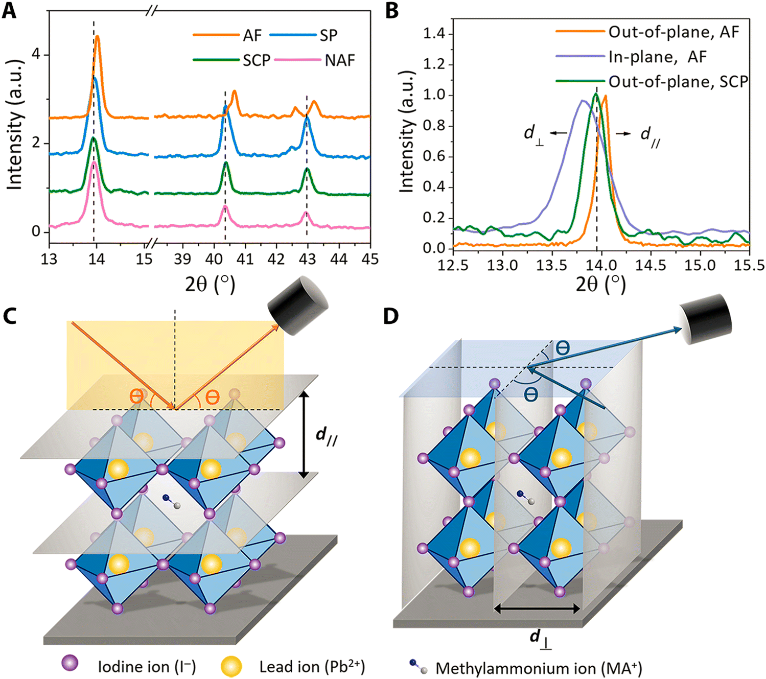
In addition to band gap engineering,44–46 strain and doping engineering have been broadly applied in the semiconductor industry to achieve fast transistors with both compressive and tensile strain. Moreover, to enhance the ferroelectric, piezoelectric and pyroelectric properties of halide perovskites, two nano-engineering approaches, i.e., strain engineering47–49 and doping engineering,49 have been proposed.It has been reported that strain is induced by the mismatched thermal expansion between the films and the substrate.56 Hence, it has also been suggested that halide perovskite films prepared by the presented techniques are strained during the thermal annealing process.56 These polycrystalline films have compressive strain in the in-plane and tensile strain in the out-of-plane direction, as shown in Fig. 1.
 | ||
| Fig. 1 Characterization of halide perovskite strain property. (A) crystal pattern, (B) plane orientation, (C) the out-of-plane XRD and (D) in-plane XRD. Reprinted with permission.56 Copyright 2017, American Association for the Advancement of Science. | ||
Furthermore, Fig. 1A shows a shift in the (110) peak towards a lower diffraction angle, indicating the presence of lattice strain. Fig. 2B shows that the (110) in-plane peak shifts to a lower angle compared to the strain-free peak of the single crystals, showing tensile strain in the horizontal direction for the polycrystalline MAPbI3 film. As shown in Fig. 1C, the spacing of the crystal planes perpendicular to the substrate was measured by out-of-plane XRD. The XRD peak shifted from a lower to higher diffraction angle, which belongs to a smaller plane spacing, and as a result the strain is compressive in the normal direction of the films. A schematic of the in-plane XRD measurement of the spacing is shown in Fig. 1D, which belongs to the larger plane spacing, and as a result the strain is tensile strain, as shown in Fig. 1B.
 | ||
| Fig. 2 Illustration showing functional relationships: reproduced with permission.57 Copyright 2013, Macmillan Publishers Limited. (1) All ferroelectrics are pyroelectrics, piezoelectrics, and dielectrics, but not necessarily the reverse; all piezoelectrics are dielectrics, but not all dielectrics are necessarily piezoelectrics. (2) Important electrical properties of materials. (A) Dielectric materials show charge separation under an electric field. (B) Piezoelectric materials show an electric polarization when stress is applied from the combination between electrical and mechanical energy. (C) Change in temperature induces a net polarization in pyroelectric materials. (D) Application of an electric field reverses the polarization in ferroelectric materials. All these materials are both piezoelectric and pyroelectric. | ||
Moreover, strain engineering is a useful mechanism for engineering strain-sensitive energy harvesting devices such as piezoelectric pressure/strain sensors, photodetectors and nanogenerators.58–60 This practical approach is essential for monitoring the optoelectronic and electronic properties of piezoelectric inorganic materials through the application of working internal or external stress. Presently, various energy harvesting devices have been fabricated using halide perovskite materials. Thus, strain engineering is useful to develop halide perovskite piezoelectric pressure/strain sensors, photodetectors and nanogenerators, as well as to solve their stability issues. Materials with mobile ions are responsible for introducing stress, and hence halide perovskites have ions showing mobility, where strain can change their activation energy. Thus, an extensive analysis and understanding of strain are required to improve the energy harvesting performance of halide perovskites.61 However, the generation of strain at the interface has been observed to reduce the performance of solar cell devices, and hence careful attention should be given not only for its usefulness but also its impact, which may cause device failure.62
Besides strain engineering, doping engineering has been proposed as alternative to improve the ferroelectric dipole ordering,49 specifically replacing I with smaller halogen anions, such as Br and Cl. This is based on the idea that substitution doping with smaller ions induces natural compressive strain on the unit cell.74,75 In addition, doping can also induce lattice strain, which is less likely upon the application of external forces.76 Specifically, the I sites in tetragonal MAPbI3 are either on the MAI layers or PbI2 layers. For example, doping of the MAI layers shortens the Pb–halogen bonds along the c axis, and decreases the c lattice parameter, while doping of Br (Cl) on the PbI2 layers shortens the Pb–halogen bonds in the ab-plane and decreases the a and b lattice parameters. Thus, to increase c = a, the ideal doping should not be on the MAI layers, rather it is better if it is on the PbI2 layers.49 For instance, Br doping on the PbI2 layers is energetically preferred to that on the MAI layers by 16 meV per unit cell owing to the presence of eight I anions on the PbI2 layer per unit cell while four on the MAI layer.49 This indicates that there is higher probability for doping to substitute iodine on PbI2 compared to MAI. A higher amount of dopant, such as Br and Cl, gets more space in the doping site where there is a higher amount of substance to be replaced or substituted, i.e. PbI2 in this case.
2.2 Polar order and domain wall engineering approach
With the perspective of enhancing energy harvesting performance, understanding the mechanisms and polar order and domain engineering play a vital role. Although polar order engineering can be applied at the A or B site in the ABX3 3D structure, domain engineering can be applied on the surface, wall and interface for heterostructure architectures such as CH3NH3PbI3/PZT. The important mechanism of ferroelectric phase transition involves order–disorder, displacive type and mixed order–disorder.77–80 Moreover, the energy harvesting performance can be enhanced using various strategies. The materials engineering strategies including stress-induced domain wall motion,81 domain wall switching,82 depolarization mechanisms, domain wall propagation, and stable domain patterns with suitable properties83 are useful for the development of energy harvester for various applications.The purpose of ferroelectric domain formation is reducing the electrostatic energy of the depolarizing fields and the elastic energy associated with the mechanical constraints to which the ferroelectric material is subjected as it is cooled through the paraelectric–ferroelectric phase transition.96 Furthermore, the surface charge induced at the onset of the spontaneous polarization with nonhomogeneous distribution and at the transition temperature generates an electric field, which is named the depolarizing field, Ed, and oriented in contrast to Ps (Scheme 1). The two important minimizing mechanisms of the electrostatic energy correlated with the depolarizing field are as follows: (1) the splitting of a ferroelectric into domains with awkwardly oriented polarization, as shown in Scheme 1, and (2) compensating a depolarizing charge by electrical conduction or by charges from a nearby substance. (3) A ferroelectric split in the crystal into domains may also take place because of the influence of mechanical stresses, as shown in Scheme 5.96,97 Essentially, there are two types of twinning in accordance with the direction of the polar axis between neighboring twinned domains in the tetragonal perovskite, i.e., perpendicular (90° domain) or antiparallel (180° domain),98 as shown in Scheme 1. Thus, a 180° phase-contrast or charged domain wall has been shown in β-MAPbI3 thin films,93 which generates a high electric field, inducing free charge buildup across the wall and intensely amplifying the domain-wall conductivity.
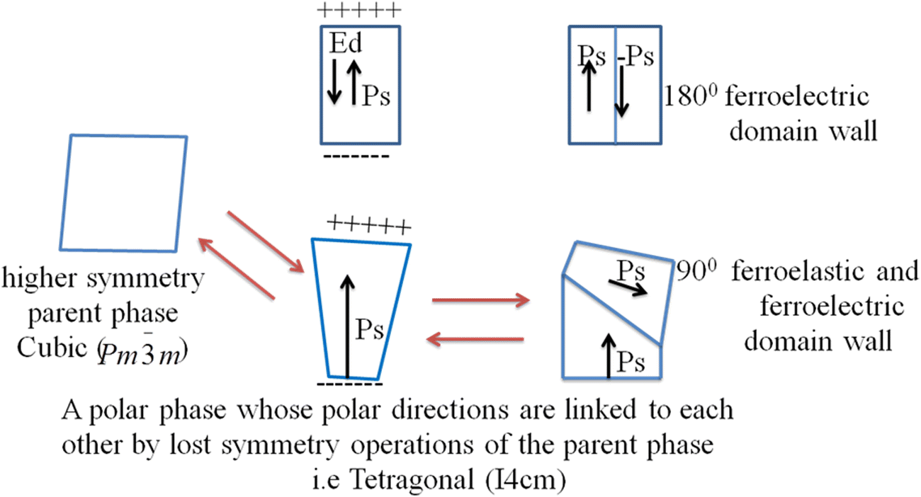 | ||
| Scheme 1 Schematic of two possible ferroelectric domain walls: domain-type 180° and 90° in a tetragonal structure. | ||
2.3 Composition engineering strategy
Important classes of materials are revolutionizing the energy harvesting research field, as already indicated by recent developments.99–101 Among them, a notable class is organic inorganic hybrid perovskites. These new molecular ferroelectric materials are superior to oxide perovskites in this field, as summarized by the Qiong Ye and Ren-Gen Xiong research group.102 Their advantages of low cost, solution processing, homochirality, biocompatibility, environmental friendliness, tunable chemical structure, and good ferroelectricity and piezoelectricity make halide perovskites encouraging for the future of high-performance energy devices.103 A precise molecular design has been suggested to engineer energy harvesting molecular perovskite families.104 This molecular design depends on the interaction of organic–inorganic cage,105 role of chemical substitution in both organic and inorganic cages,76,106–108 role of polar phonon interaction,109,110 composition (or mixing) based on ratio of atoms,111–116 polar order and domain wall,98,117–119 chirality of organic cations,120 spin–orbit coupling,121 hydrogen bonding,122 cation ordering,123–127 doping effect,29 and quantum and dielectric confinement.128 Confinement engineering has also been reported to design 2D lead halide hybrid perovskite ferroelectrics.129 Materials with multifunctional properties are greatly required to develop multifunctional devices that respond upon exposure to various external stimuli. These multiferroics are due to the coexistence of two or more properties in a single material such as magnetism and ferroelectricity, switchable dielectric and thermochromic luminescence properties as well as photovoltaic and optoelectronic properties observed in hybrid halide perovskites.130,131 However, owing to the coexistence of multiple properties in halide perovskites, it is not yet known whether these multiple properties are mutually inclusive or exclusive. Ferromagnetism and ferroelectrics are mutually exclusive because ferroelectrics need empty d orbitals, while ferromagnetism requires full d orbitals. Moreover, the coexistence of ferroelectricity/superconductivity/polarity has not been discovered to date. Thus, the ferroelectric property of halide perovskites is composition dependent, as summarized in Table 1.| Material | E g/eV | d 33/pC N−1 | P s/μC cm−2 | T C/K | Young's modulus/GPa | Symmetry change |
|---|---|---|---|---|---|---|
| HC(NH2)2+ = FA, trimethylbromomethylammonium = TMIM, MDABCO = N-methyl-N′-diazabicyclo[2.2.2]octonium, ChPy = chloropropylammonium, 3-AP = 3-ammoniopyrrolidinium, TMFM = trimethylfluoromethyl ammonium, and TMCM = trimethylchloromethyl ammonium. | ||||||
| (TMFM)x(TMCM)1–xCdCl3132 | — | 1540 | — | 366.8 | — | — |
| MAPbI39,133 | 1.56 | — | 7.2 to ∼8 but 38 is expected | 330 | E[100] = 10.4 | I4cm to Pmm |
| BaTiO3134 | — | 190 | 26 | 393 | — | — |
| Tetragonal to orthorhombic MAPbBr3135 | 2.2 | — | ∼0.35 to ∼0.4 | — | — | Pna21 to I4cm |
| CsPbI3136,137 | 1.73 | — | — | — | 186 | Pnma to Pmn21 |
| MAPbI3−xClx138 | 1.57 to 1.63 | — | — | — | — | — |
| NH4PbI3110 | 1.76 | — | 5.4 | — | ||
| (ChPy)4AgBiBr8139 | — | — | 3.2 | 305 | — | — |
| (MDABCO)RbI3140 | 14 | 22 | 448 | R3 to P432 | ||
| MPSnBr3141 | 2.62 | — | 4.5 | 357 | — |
Pna21 to Pm![[3 with combining macron]](https://www.rsc.org/images/entities/char_0033_0304.gif) m m |
| 3-APRbBr3142 | — | — | — | 440 |
Pmm to Ia |
|
| MDABCONH4X3 (X = Cl−, Br− and I−)107,143 | 119, 248 and 178 | — | 14.7 | — | ||
| MHy2PbBr4139 | — | — | 5.8 | 351 | — | Pmn21 to Pmnm |
| MAPb(I1−xBrx)3144 | — | — | — | — | — | |
| CH3NH3SnI3145 | 1.30 | — | — | — | — | — |
| N(CH3)4SnI3146 | 2.12 | — | 16.13 | — | — | R3m |
| FAPbI3147 | 1.47 | — | — | E[100] = 11.8 | P 3 m 1 ↔ P63mc | |
| MAPbCl3102,148–151 | 2.9 | — | — | — | E[100] = 19.8 | — |
| TMIM-PbI315 | — | — | 0.67 | 312 | — | C 2 ↔ C2/m |
3. Microscopic mechanisms and origins of new property
To develop high-performance energy harvesting halide perovskites devices, understanding both the macroscopic and microscopic properties of these materials is highly required. Parameters such as pressure, texture, colour, volume, density, and temperature are considered macroscopic properties, while quantum states, atomic mass, electron spin, molecular bond lengths, and bond energies of individual particles are considered microscopic properties. The macroscopic properties of halide perovskites have been thoroughly studied,152 whereas their microscopic properties still require detailed investigation. Accordingly, this section mainly focuses on discussing the microscopic properties of halide perovskites. This will give researchers insight into their microscopic properties for the development of new energy harvesting and emitting devices. Notable advantages of halide perovskite materials are their low-cost solution-based synthesis method,153 exceptional quantum yields and structural and compositional tunability.154 However, although halide perovskites are easy to synthesize, they are difficult to handle. This is because of their degradation and unstable property when exposed to oxygen and moisture.152,155,156 Irrespective of these problems, halide perovskites show promise for a wide range of energy harvesting and emitting applications. What is the origin of these wide-range potential energy harvesting, photosensing and nano-sensing applications? To elaborate on this big question, understanding the microscopic origins and mechanisms of multifunctional properties is a vital and cannot be ignored. This is the big issue we want to present for the betterment of the current energy harvesting multifunctional properties of halide perovskites (Scheme 2).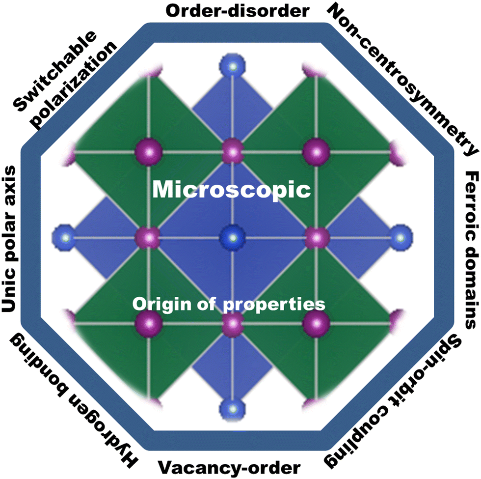 | ||
| Scheme 2 Microscopic origins and mechanisms of multifunctional property of halide perovskites. | ||
Energy harvesting piezoelectric materials will be considered be safe if they are non-toxic, stable, have an acceptable curing temperature and easy poling treatments for practical applications. Thus, efforts have been devoted to searching for materials that are non-toxic, stable, and have a high curing temperature and easy poling treatments.157 Energy harvesting halide perovskites have limited practical applications because of their toxicity, instability, bias-induced material degradation158 and unexpected inconsistency in forward–backward I–V characteristics.159 Also, some reports indicate that halide perovskites possess a low curing temperature and difficulties in poling treatment owing to their switchable spontaneous electric polarization.160 Furthermore, ionic diffusion contribution has been detected, causing increased radiative recombination.159
From the view point of discovering new energy harvesting materials, materials with a large proof mass displacement, high strain and tolerance to high strain are required.161 Thus, materials that are not fragile but have high elasticity property are more attractive for piezoelectric energy harvesting. For instance, polyvinylidene fluoride (PVDF) fulfills this requirement. All these requirements will maximize the energy transduction. Alternatively, thermoelectric energy harvesting requires a low thermal conductivity, K, high Seebeck coefficient, α and high electrical conductivity.161 For this purpose, low phonon materials and scalable fabrication methods are required.162 Not only piezoelectric and thermoelectric effects but also the pyroelectric effect are important for energy harvesting. In pyroelectric energy harvesting, both temperature changes in time and polar point symmetry are required, as is known by researchers. As green energy sources, energy harvesting materials need to have piezoelectric, thermoelectric and pyroelectric properties, based on which energy is collected to fulfill the human energy demand. Furthermore, to enhance the efficiency of harvesting, the quality factor is required. The higher the quality factor, the lower the heat loss and less damping in energy conversion, boosting the efficiency of the energy harvester.
The successful properties of halide perovskites originate from both macroscopic and microscopic properties. Their macroscopic properties arise from the arrangement and interaction of the constituent cages, while their microscopic properties emerge from the behavior and interaction of atoms, molecules and ions. In particular, the macroscopic properties are the properties of a substance or matter that can be identified with naked eye and measured with no change in its chemical identity. The mechanisms of action of the microscopic origin and property–functionalization of a given material are atomic and molecular properties such as bond energies, atomic mass and molecular bond lengths, causing order–disorder, organic–inorganic interactions, spin–orbit coupling, hydrogen bonding, switchable polarization, local noncentrosymmetry, dipole ordering, multiple polarization directions, ferroelectric domain, polarization, structural transition, unique polar axis, etc.102,110,163–167 This indicates that understanding both the macroscopic and microscopic properties of halide perovskites can lead to their multi-functionalization in a wide range of applications. Thus, researchers should deeply investigate both properties for the betterment of this field for suitable applications. For instance, ions such as Bi3+ ions and Pb2+ have two lone pair electrons in their 6s orbital. These electrons do not play any role in chemical bonding, but their order of lone pairs has the ability to determine the microscopic origin of ferroelectricity.168
3.1 Order–disorder property
Order–disorder phenomena occur in crystals in which two or more energetically and structurally nonequivalent sites are occupied by two or more vacancies, ions, atoms, or other particles. In some cases, this order–disorder is linked with an “inversion” or first-order phase change, which encompasses a change in crystal symmetry.169 The order–disorder property is responsible for the soft mode phonon and dielectric constant. Ideally, if the order parameter indicates phase transition behavior, then there is order–disorder property. In this case, the local distortion remains unchanged. This means that the octahedral structure remains stable. To confirm this property, X-ray absorption fine structure (XAFS) studies are required. Recently, there have been reports regarding this order–disorder property in halide perovskite materials.168,170–1753.2 Hydrogen bonding and emerging van der Waals
The presence of hydrogen in halide perovskites has been reported elsewhere.176,177 Also, α- and β-type hydrogen bonding have been detected.178 The α-interaction mode determines the stability of the octahedral network.179,180 This hydrogen bonding has an essential contribution to the optical, structural and electronic properties of halide perovskites.181 In addition, hydrogen bonding facilitates outstanding decoupling of the crystal growth process and nucleation.182 It has also been reported that hydrogen bonding stabilizes the structure of CH3NH3PbBr3.183 In addition to the presence of hydrogen bonding, emerging van der Waals interactions are important in halide perovskite research. These van der Waals interactions are responsible for the presence of ferroelectric properties in certain materials in terms of switching kinetics, polar stabilization and polarization origin.1843.3 Switchable polarization property
In addition to order–disorder and hydrogen bonding, switchable polarization (polar order) is an indicator of the presence of ferroelectric properties. In halide perovskites, the presence of this property has been detected.11,185–187 This reversible polarization is carrier activated and affected by organic molecular dipoles when exposed to light.188 The mechanism of light-induced polarization is light-induced free carriers due to carrier-induced lattice distortion, leading to the formation of polarons, which occurs below the Curie temperature.189,190 The arrangement of anions and cations upon the application of an electric field creates a dipole moment, which acts as the source of polarization. This dipole moment has ordered polar electric dipoles from which ferroelectricity originates upon polarization. This is measured by measuring the surface current of a ferroelectric material. Therefore, this switchable polarization is expected to make halide perovskites suitable for electro-optic devices, actuators, nano-electronics and memory applications. To achieve successful application, priority towards understanding the nature of this switching polarization is required. For simplicity, elastic strain, domain size and domain wall energy are joint features that govern the nature of switching polarization.1913.4 Unique polar axis
The unique polar axis is an axis where spontaneous polarization takes place at the Curie temperature. However, its direction can be reversed with the application of an external electric field. Researchers indicated that only ten point groups have a unique polar axis, which is responsible for the presence of ferroelectrics.192 Thus, halide perovskites are materials that have unique polar axis responsible for their spontaneous electric polarization-induced ferroelectric properties.3.5 Local non-centrosymmetry property
Halide perovskites have non-centrosymmetry property,193–195 and the presence of this unique property makes them applicable in ferroelectrics, circular dichroism, pyroelectrics, nonlinear optics, circularly polarized photoluminescence, etc.196 The idea of non-centrosymmetry is separating the center of negative and positive ions to cause permanent polarization in a given material. This polarization is reversible under an applied external electric field. The microscopic origins of ferroelectric properties upon the application of an external electric field are the nucleation and growth of domains. These domains are known as ferroelectric domains. Ferroelectric materials have distinct areas about 1 μm thick and domains where polarization happens homogeneously.197 Because of these properties, halide perovskites are ferroelectric in nature.3.6 Ferroic domains
Ferroelectric domains are generated when there is a unit cell retaining polarization having identical orientations. An electric field drives domain wall motion, which activates changes in the orientation and size of the domain. Furthermore, this can be employed to compare the topography of a sample with other local material properties, such as piezoelectricity, conductivity and electrical potential to investigate the microscopic origin of these effects.198–201 Especially, piezoresponse force microscopy (PFM) is an AFM tool because of the converse piezoelectric effect, which can locally probe the electromechanical properties of piezoelectric samples. Given that ferroelectricity is often paired with piezoelectricity, PFM can also image ferroic domains.200,201 Numerous researchers have conducted PFM studies on MAPbI3 films.93 However, the results of these reports were paradoxical. Furthermore, switchable ferroelectric domains have been demonstrated, which were also supported by subsequent PFM studies.202,203 Nevertheless, it has also been suggested that there was no proof of ferroelectricity based on PFM.204 In recent times, two reports argued that MAPbI3 does not show ferroelectricity at RT according to macroscopic polarization methods and advanced techniques such as PFM measurements.11,205The latest findings47 revealed that coupling of nanoscale techniques and microscopic offers solid proof for the presence of ferroelastic domains in both CH3NH3PbI3 single crystals and polycrystalline films in the pristine state and under applied stress. Furthermore, experiments explain that the design of CH3NH3PbI3 ferroelastic domains in polycrystalline films and single crystals can be managed with applied stress, recommending that strain engineering may be utilized to tune the properties of these materials.47 Given that the ferroelastic domain boundaries may differ from regular grain boundaries, no proof of concomitant ferroelectricity was experiential and the discovery of ferroelasticity gives an original parameter to consider in the mission for enabling their widespread adoption and enhancing their stability. This indicates that grain boundaries have an impact on the long-term stability of halide perovskite solar cell devices.47 The PTIR technique has been used to continuously characterize the domains at the nanoscale and in situ examine whether they are vulnerable to electrical bias,206,207 attracting much attention for label-free composition mapping,208–211 material identification,212 and conformational analysis213,214 at the nanoscale.
3.7 Rashba and Dresselhaus effects
The interaction between the orbitals in motion and the electron spin round the nucleus is spin–orbit coupling, where this phenomenon is the core of spintronics and magnetism by driving magnetic damping, spin relaxation and magnetic anisotropy.215 This application motivated researchers to devote their efforts to investigating halide perovskites. For this purpose, MAPbI3-based spin-optoelectronic devices have been reported.216 Highly spin polarized magnetization has been reported for MAPbI3.217–219 Exotic spin-splitting phenomena, for instance, Dresselhaus and Rashba effects,220–224 are usually observed in the relativistic electronic structure of nonmagnetic semiconductors.225–227 This phenomena may arise due to spin–orbit coupling (SOC), the presence of relatively heavy elements and the non-centrosymmetry of ferroelectric materials. The “dynamical Rashba effect”, which is present in even universal centrosymmetric structures, has been revealed by molecular dynamics simulations. The combined inorganic–organic degrees of freedom can generate a spatially modulated Rashba effect, which is differentiated using the MA dynamics at the sub-picosecond time scale.121,228–230 This recommends that the local non-centrosymmetry owing to the local ordering of dipoles at the unit cell scale is still a vital question to consider, although universal centrosymmetry may occur at the macroscopic scale. Nevertheless, the theoretical simulation of halide perovskites is enormously difficult given that it engages the treatment of numerous subtle, but vital aspects that are complex to determine precisely.Moreover, considering the relaxed unit cell structures suggested in the literature109 and the supposition of total organic cation ordering, Hu et al.164 calculated the spin–orbit splitting in energy band structures and the principally likely electric polarization. This is of enormous significance because Rashba splitting has been proposed to decrease the electron–hole recombination rate and enlarge the carrier lifetime.228,231,232 Hence, Hu and coworkers164 calculated the spin–orbit energy-band splitting for all 12 ABX3 relaxed structures. However, the obvious tendency among the magnitude of the atomic spin–orbit splitting, ferroelectric polarization, and analogous Rashba parameters was challenging to deduce, owing to the difficult relationship between the organic cation/framework atomic relaxations and electronic structure. The spin conduction bands and valence properties are vital for reducing the anticipated spin-splitting parameters for the entire sequence of halides and the recombination rate can assist the comprehension of the fundamental characteristics of the exceptional functionalities of halide perovskites solar cells. The Rashba effect is explained using the supposed Bychkov–Rashba Hamiltonian, as in eqn (1), which is the outcome of the breaking of inversion symmetry in the crystal in a direction orthogonal to a k-point sampling plane.227,233,234
 | (1) |
3.8 Vacancy-ordered perovskites
Owing to their ion migration, ferroelectric, pyroelectric, piezoelectric and optoelectric properties, halide perovskites become a hot research topic. Besides, their flexibility to integrate into systems, high energy density and vacancy-ordered properties make halide double perovskites applicable in energy storage and energy harvesting devices, as demonstrated by double halide perovskites such as MA2SnX6 for Li ion batteries,100 Cs2NaBiCl6 for batteries, TMCM2SnCl6 for nanogenerators241 and Cs2SnI6 for transistors.242 Moreover, the development of high-power rechargeable batteries requires high mobility of Li+ to overcome the diffusion barrier. Thus, Sn-based double halide perovskites have periodic Sn vacancies narrowing the diffusion barrier in materials such as MA2SnX6 for Li ion batteries.100 Hence, these periodic metal vacancies are highly useful for high efficiency Li-based metal batteries, with further research revolutionizing the area of storage devices.4. Multifunctional properties beyond ferroelectrics
Halide perovskite-based solar cells have been revolutionizing the field of photovoltaics with a power conversion efficiency of 29.13%,243 breaking the maximum limit for silicon solar cells. This is because of their interesting properties such as tunable light absorption, superior charge-transfer properties, tunable band gaps, short diffusion length and facile processing.244–248 Beyond photovoltaics, there are other fascinating applications due to their new promising properties such as ferroelectrics, piezoelectrics, pyroelectrics and coexistence of multiple properties.249 Interestingly, the coexistence of two or more properties makes materials suitable for a wide range of applications such as in photovoltaic, optoelectronic, thermoelectric, magnetism, ferroelectric and magneto-ferroelectric applications simultaneously. For this purpose, the multifunctional properties of halide perovskites of both types, organic inorganic hybrid halide perovskites and all inorganic halide perovskites, will be discovered for a wide range of applications. Moreover, the coexistence of multiple properties still has to be discovered, and thus needs more attention. Because of this, some research has been reported.250–255 As shown in Scheme 3, halide perovskites are multifunctional materials required for various applications. | ||
| Scheme 3 New operating stimuli and operation mechanisms with new electrical property for new electromechanical and electronic applications proposed for the field of halide perovskites. | ||
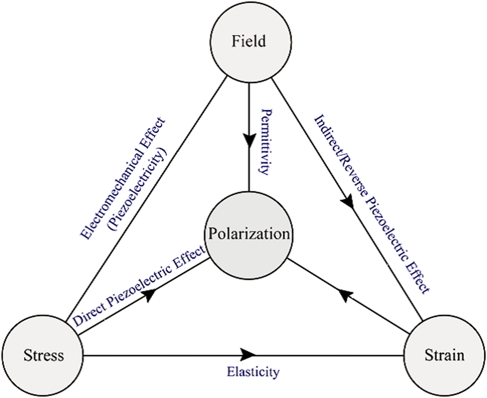
Before directly discussing the details of ferroelectric, pyroelectric, piezoelectric and dielectric properties of halide perovskite materials, it is of great interest and importance to present an overview of these electronic properties first. Accordingly, to maintain the analogy, the term “paraelectric” should properly refer to polar dielectrics, which consist of grains with polar regions oriented randomly in a solid, resulting in no net dipole moment (i.e., no net polarization). This phenomenon is the electrical equivalent of paramagnetism, and generally describes the condition of virgin (unpoled) ferroelectrics below the Curie temperature, TC. Because the grains/domains are polar, they are also piezoelectric. All but one of the 21 non-centrosymmetric crystallographic point groups are piezoelectric (the symmetry elements combine in the cubic group 432 to yield no net piezoelectric effect). Furthermore, ten of the 21 non-centrosymmetric groups include a distinctive polar axis, and consequently suddenly polarized. These are the “pyroelectric” materials, in which a variation in temperature results in a variation in polarization. The reverse process is called the “electrocaloric” effect.256 Several pyroelectric materials have an extra property that the direction of impulsive polarization can be varied by mechanical stress or applied electric field. When it is primarily due to stress, it is “ferroelastic”, whereas when the variation is mainly owing to an electric field, the material is “ferroelectric”.
A piezoelectric or pyroelectric is not necessarily ferroelectric, but all ferroelectric materials are pyroelectric and piezoelectric, as shown in Fig. 2(1). Ferroelectric materials above their TC are generally called “paraelectric”, even if the similarity between ferroelectricity and ferromagnetism falls apart here. Although a ferroelectric would lose its dipoles altogether above TC and become a non-polar dielectric, a ferromagnet would become paramagnetic above TC. This material is centrosymmetric, and thus includes no dipoles at all; however, polarization can be induced by an external field in such a way as to expel or reduce the electrostatic energy from the solid. This incidence is fundamentally the electrical equivalent of diamagnetism except that diamagnetism would also have negative susceptibilities. Moreover, coexisting properties should also be studied in the field of the halide perovskites.257,258
Moreover, the intrinsic electric polarization character of ferroelectric materials can be altered by an applied electric field. Nowadays, ferroelectrics have become highly attractive for several technological devices that utilize their pyro-, piezo-and ferroelectric properties (Fig. 2(2)), with great functionalities possible for ferroelectric non-volatile memories.259 These materials normally undergo a phase transition into a low-temperature ferroelectric (polarized) state at the Curie temperature, TC, from a high-temperature non-polarized paraelectric state,260 which results in spontaneous polarization. This is due to the structural transition and usually small symmetry-breaking distortion occurring at TC. Low-temperature ferroelectric materials always show a non-centrosymmetric structure, and consequently they do not exhibit inversion symmetry, given that this averts the charge separation intrinsic to the electric polarization.261 An additional event in which an electric field provides a variation in dimensions is electrostriction, which is a quadratic effect between mechanical strain and electric field and can be observed in all dielectric materials, while piezoelectricity follows a linear relationship.
Ultimately, ferroelectric materials provide highly valuable properties such as ferroelectric hysteresis, high permittivity, high piezoelectric and pyroelectric coefficients, strong electro-optic effects and anomalous temperature coefficients of resistivity. Among these properties, the formation of a hysteresis loop is a highly imperative property of ferroelectric materials due to its polarization reversal property.262 Furthermore, this behavior originates with the use of an electric field and a cycling process is observed through the positive and negative directions in ferroelectric materials, as presented in Fig. 3.
 | ||
| Fig. 3 Polarization hysteresis loop. Reproduced with permission263 Copyright 2015, Michele Manzo, Doctoral Thesis. | ||
E c depends on the defect concentration, temperature, voltage waveform, surface, electrodes, mechanical pressure and stoichiometry. The polarization originally amplifies from zero to a saturation polarization, Ps, leading to a decline in the electric field, and decreases to remnant polarization, Pr, as revealed in Fig. 3. Furthermore, the electric field needed to decrease the polarization back to a zero value is termed the coercive field, Ec.
4.1 Tunable material composition
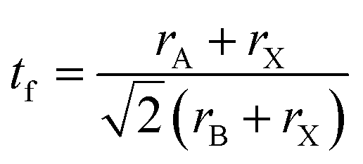
The wide range electronic, structural, magnetic and optical properties of halide perovskites originate from their tunable chemical composition and dimensions (1D, 2D and 3D).195 This tunable property makes halide perovskites possess reasonable multifunctional properties for various applications such as ferroelectricity, photovoltaics, thermoelectrics, optoelectronics, ferromagnetism, photocatalysis, storage devices, self-powered units and wireless electronics. These tunable properties are comparable electron and hole effective mass, point defects, grain boundaries, high optical absorption and electrically clean defect properties.264 Moreover, the great attention towards energy harvesting piezoelectric materials is owing to their flexibility to be incorporated into systems and promising energy density compared with electrostatic and electromagnetic devices.265 Thus, the piezoelectric properties of halide perovskites have attracted greater attention for various energy harvesting applications. The high energy density of piezoelectric materials is owing to their highly crystalline structures, giving dipole moments and nonoverlaping centers of negative and positive charges.265With respect to this general overview, the halide perovskite family is under study this time. This is due to their tunable crystal structure ABX3 and corner-sharing BX6 octahedra with a B site cation in the middle, in addition to their tunable chemical composition, where ‘A’ and ‘B’ are two cations of different sizes with +1 and +2 valence, respectively, and ‘X’ is a halide anion, which forms bonds with both A and B. The stability of the halide perovskite structure is described by the Goldschmidt tolerance factor, t, as defined as in eqn (2), as follows:
 | (2) |
 | ||
| Scheme 4 Representation of stress and field-induced electrical properties of OMH perovskite materials. | ||
Understanding and identifying the unit and important parameters related to the paraelectric, piezoelectric, pyroelectric and ferroelectric properties of currently reported organic inorganic hybrid perovskites is essential in this field.102 Therefore, this unit and important parameters regarding the ferroelectric and piezoelectric properties of organic inorganic hybrid perovskites are reviewed well elsewhere. These parameters are crucial to understand the ferroelectric functional and structural diversity of these materials. This indicates that there are various organic inorganic hybrid perovskites for various applications in the practical thermoelectric applications.
4.2 New ferroelastic properties
Another important electrical property of perovskite materials is their ferroelastic phase transition, which shows a way to distort their crystal lattice, resulting in spontaneous strain in the material, which is similar to the magnetization/spontaneous polarization in ferromagnetic/ferroelectric materials.166 Upon the application of external stress, this spontaneous strain can switch its direction in the crystal lattice.266 Thereby, the formation of twin domains oriented along different crystalline axes lowers the internal strain. For instance, a tetragonal structure shows spontaneous strain orientations along the a1, a2 and c axes.267 Similar to ferroelectricity, ferroelasticity and magnetoelasticity268,269 are usually viewed in perovskites with an ABX3 structure and is a nonlinear property.266,267 Recently, ferroelectricity has been suggested to be a possible mechanism to clarify the high PCE in halide perovskite solar cells; however, realistic experimental proof supporting this premise is lacking. Distinguishing and identifying ferroelectricity as another characteristic, for instance piezoelectricity and ferroelasticity, is normally appreciable given that this occurrence can coexist in many materials.Ferroelastic twin boundaries as typical grain boundaries have been identified in CH3NH3PbI3.270 These ferroelastic twin boundaries neither influence the charge carrier dynamics nor behave as non-radiative recombination centers but easily fade.270Fig. 4a–c show the X-ray diffraction peak (a) and images of an MAPbI3 single crystal using a polarized optical microscope (c), while Fig. 4d–f show optical images of the domain pattern in an MAPbI3 single crystal using polarized light before the application of external stress (d), under tensile stress (e), and after reliving the stress (f).
 | ||
| Fig. 4 Polarized optical microscopy confirming presence of ferroelastic domain pattern in MAPbI3 domains. X-ray diffraction peak (a) and images of the MAPbI3 single crystal using polarized optical microscope (b–c), optical images of domain pattern in MAPbI3 single crystal using polarized light before the application of external stress (d), under tensile stress (e), and after reliving the stress (f). Reproduced with permission.270 Copyright 2020, Nature Publishing Group. | ||
The change in the stripe pattern beneath the external tensile stress confirmed the ferroelastic nature of the MAPbI3 domains. Moreover, the presence of hysteresis behavior for the motion of these ferroelastic domains was confirmed by the domain boundaries that did not completely return back to the original location after release of the applied strain.
| xij = sijklXkl | (3) |
4.3 New piezoelectric properties
Similar to ferroelectrics, it is of great interest to study and understand the piezoelectric properties and applications of halide perovskite materials. Initially, the word piezoelectric is used to explain the attractive property of an technologically important class of materials with diverse functionalities, ranging from ultrasound transducers, fuel injectors and waveguide devices to gyroscopes and accelerometers.276–278 It is of high technological interest to explore the piezoelectric properties of hybrid perovskites for applications such as piezoelectric generators and energy harvesting devices.279 In this section, the origin of the piezoelectric and piezoelectric properties, methods to enhance the piezoelectricity of hybrid perovskites, possibility of constructing dampers and low loss piezoelectric devices, and issues that should not be missed during the study of piezoelectric properties and others important points are discussed in detail.In recent times, CsPb2Br5/PVDF composite-based piezoelectric nanogenerators have been reported with working process.280 The addition of CsPb2Br5 to PVDF enhances the current and output voltage, indicating the generation of a self-poled composite that does not need additional poling.280 Thus, halide perovskites have great advantages in increasing the poling effect when added to materials. Moreover, metal halide perovskites have been reported as applicable piezoelectric materials for the fabrication of nanogenerators, as shown in Fig. 2.281 The result showed a molecular piezoelectric coefficient (d33) of 165 pm V−1 and maximum peak power density of 43 μW cm−2 at 50 kPa. This is the largest power reported for energy harvesting for EDABCO-CuCl4-based piezoelectric materials. The advantage was obtained from increasing polarization through the lattice distortion of CuCl42−. This polarization effect increased the dielectric constant, resulting in a trade-off between d33 and g33.281Fig. 5a shows the Cu2+-3d orbitals as a projected density of state for EDABCO-CuCl4, where a single state dxy and two double-degenerate states, dxz and dyz, are obtained from the splitting triple-degenerate t2 d-levels. Similarly, single states dz2 and dx2−y2 are obtained from the splitting double-degenerate e d-levels. This indicates the presence of Jahn–Teller lattice distortion. Adding a quasi-spherical cation to this lattice distortion causes enhanced mechanical response, giving a large d33.
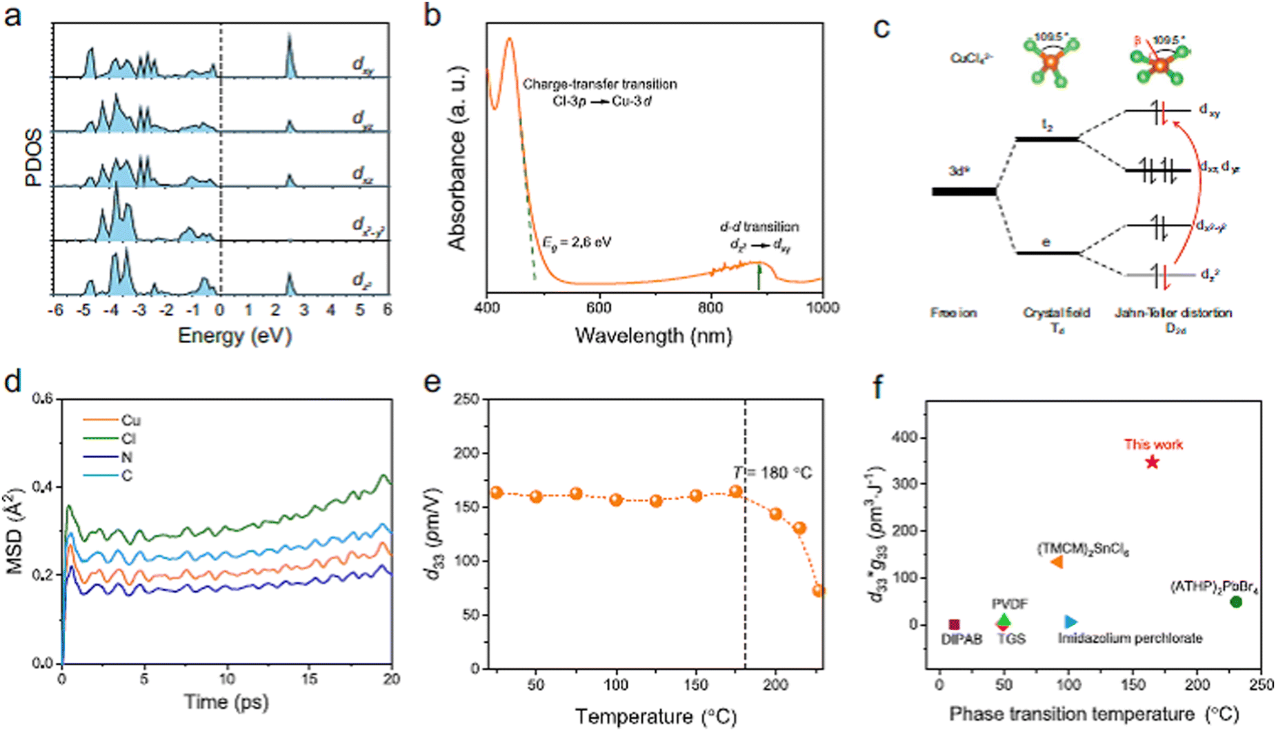 | ||
| Fig. 5 Electronic structure and piezoelectric response of EDABCO-CuCl4. (a) Cu2+−3d orbitals as a projected density of state for EDABCO-CuCl4, (b) two intense bands as referred by the optical absorption spectrum, (c) the splitting of the Cu2+−3d orbital energy level, (d) stable structure of EDABCO-CuCl4, (e) mechanical flexibility for EDABCO-CuCl4, (f) transduction coefficient (g33*d33). Reproduced with permission.281 Copyright 2023, Nature Publishing Group. | ||
Fig. 5b also shows two intense bands in the optical absorption spectrum. Although the ligand-to-metal charge transfer is observed in the visible band at 2.6 eV, the d–d electronic transitions are observed at the near infrared peak within the crystal field of [CuCl4]2−. This is caused by the Jahn–Teller lattice distortion. The splitting of The Cu2+-3d orbital energy level is shown in Fig. 5c, while the stable structure of EDABCO-CuCl4 is indicated in Fig. 5d. Furthermore, 165 pm V−1 value of high d33 of was obtained as a function of temperature, indicating enhanced mechanical flexibility for EDABCO-CuCl4 (Fig. 5e). Fig. 5f shows the transduction coefficient (g33 × d33), where the electrical energy of the energy harvester depends on the trade-off between the piezoelectric voltage coefficient (g33) and piezoelectric charge coefficient (d33).282,283 It should be noted that the trade-off between the piezoelectric voltage coefficient and piezoelectric charge coefficient for molecular metal halides is not fixed thus far, which requires further in-depth study.
| ΔPi = dijσj | (4) |
| ΔPi = eijηj | (5) |
| ΔP3 = e33η3 + e31(η1 + η2), | (6) |
 | (7) |
 | (8) |
To disclose the source of piezoelectricity,289 it is important to split the total polarization originating from contributions of the (1) A-site MA cations and (2) B-site Pb atoms. The Pb atom-induced polarization is measured using (Pb) × D(Pb)/Vu × PPb = Z33,10 where 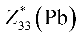 is the Born effective charge of Pb, D(Pb) is the average displacement of Pb along the c axis with respect to the center of its I6 cage and Vu is the volume of the primitive unit cell. Thus, +4.24 is the measured value from the contribution of
  , which is considerably greater than the supposed charge of Pb (+2.0) in a pure ionic image.10 This implies the presence of dynamic charge transfer coupled with a change in the Pb–I bond length and strong covalence of the Pb–I bonds. It is obvious that both molecular dipoles and Pb displacements are responsible for the total polarization, in which Pb atoms contribute nearly all the piezoelectric response, with a negligible contribution from the MA+ molecules.
In perovskites with unusual atomic substitutions in the ABX3 architecture, the competition between the B–X metal–halide bond and A–X hydrogen bond determines their piezoelectric characteristics, drawing attention to the prospective of halide perovskite design for manipulating useful photopiezoelectrics and photoferroelectrics,10 such as applications in sensors, actuators, and energy harvesting.278,280,290,291 Because of the pairing of semiconducting properties with piezoelectrics, micro- and nanowires of piezoelectric semiconductors have been utilized as fundamental building blocks for developing ground-breaking devices,292 for instance, piezo-phototronic devices,293,294 piezoelectric diodes,295 piezoelectric field-effect transistors,296 piezoelectric chemical sensors297 and nanogenerators.298–300
Halide perovskites possesses a cubic crystal structure that gives rise to ferroelectric polarization similar to other classes of perovskites with identical structural characteristics.301,302 Coll et al. demonstrated the polarization switching and light-enhanced piezoelectricity of CH3NH3PbI3 materials.11 Furthermore, output piezoelectric values of 2.7 V and 140 nA cm−2 have been reported,15 hindering practical functionalities due to their modest output performance. Moreover, the highest piezoelectric current density and output voltage of 3.8 μA cm−2 and 8.5 V have been demonstrated by a piezoelectric nanogenerator under periodically vertical compression. Multilayered halide perovskites even have larger large polarization or strong piezoelectricity of ≈1540 pC N−1.303 This output is quite promising compared to other literature reports,14 which can help charge LEDs and capacitors through a bridge rectifier.
 | ||
| Fig. 6 Schematic of the domain engineering for piezoelectricity enhancement strategy. Reproduced with permission.304,305 Copyright 1997, IOP Publishing. Note that larger d15 is a key factor for oxide perovskites but larger d15 is not well defined whether it is a key factor for halide perovskites. | ||
A d33 value of 2.7 pm V−1 for MAPbI3 single crystals has been found,306 which is close to the value for quartz (∼2.0 pm V−1),307 but considerably lower than the values for Pb(Zr,Ti)O3 (∼400 pm V−1)308 and ZnO (∼12 pm V−1).309 Additionally, PFM has been used in polycrystalline thin films to confirm the local d33 value of 6 pm V−1.11 To date, no effective material strategy has been developed to engineer the polar axis of piezoelectric response. In the case of an MAPbI3 film on Au and ITO, the d33 value is ∼0.3 pm V−1, which is almost two orders of magnitude lower than that of PZT.310 Recently, the piezoelectric coefficient was found to be ∼4 pm V−1 for both polarization directions, with no appreciable dependence on the film thickness.310 Alternatively, the films on Au and ITO revealed a consistently low d33 value of about 0.3 pm V−1. This value is about one order of magnitude lower than that obtained on the bulk single-crystal samples. Notably, in 1969, physically powerful piezoelectricity was demonstrated in poly-vinylidene fluoride (PVDF) materials. Since then, PVDF has been used for a variety of functionalities in comparison to PZTs because of its lower cost, accessibility and other piezoelectric parameters. When poled, PVDF is a ferroelectric polymer, showing competent piezoelectric and pyroelectric characteristics. These properties make it suitable in sensor and battery functions.311 Therefore, the use of this material and its derivatives may be an important research direction for the piezoelectric enhancement of halide perovskite materials. There are also numerous other synthetically fabricated piezoelectric materials such as active fiber composites (AFC) and Quick Packs™, which are flattering and more accessible for different functions. However, Lee et al.312,313 performed experiments to contrast PVDFs and PZTs for energy harvesting functionalities and found that PVDF with a certain electrode configuration had the longest fatigue life, and hence is more suitable for energy harvesting.
![[thin space (1/6-em)]](https://www.rsc.org/images/entities/char_2009.gif) ϕ, piezoelectric tanθ, and dielectric tanδ, where θ′ is obtained in the k31 mode (eqn (9)), as follows:304
ϕ, piezoelectric tanθ, and dielectric tanδ, where θ′ is obtained in the k31 mode (eqn (9)), as follows:304 | (9) |
ϕ′ is obtained from the inverse value of QA in the k31 mode, whereas tanδ′ is obtained from a capacitance meter at a frequency or impedance analyzer away from the antiresonance range or resonance.316 Furthermore, parameters from an admittance/impedance spectrum around the antiresonance (B-type) and resonance (A type) range are obtained experimentally including ωa, ωb, QA, QB (from the 3 dB bandwidth method), and the normalized frequency Ωb = ωbl/2v. The electromechanical coupling factor k is calculated using ωa and ωb and the IEEE standard equation in the k31 mode, as follows in eqn (10):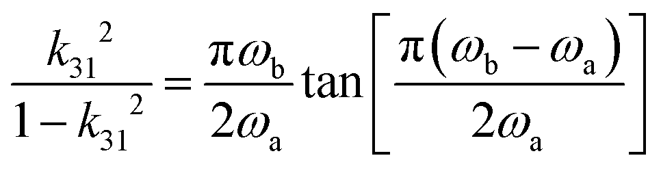 | (10) |
 | (11) |
 | ||
| Scheme 5 Representation of proposed factors affecting piezoelectricity. All factors affecting ferroelectricity affect both piezoelectricity and pyroelectricity. | ||
 | (12) |
 | (13) |
 | (14) |
Alternatively, the piezoelectric coefficient can also be determined for layered heterostructures such as MAPbI3/PTZ layered heterostructures, in which the greater part of the bias voltages was constantly applied in the course of the MAPbI3 layer, in which the fraction of voltage (νMAPbI3 = VMAPbI3/Vbias) varied between 87% and 93% because of the enhancements in film thickness from 20 nm to 60 nm.310 Once the voltage fractions across the two layers (νPZT = VPTZ/Vbias) have been determined, the d33 value of MAPbI3 can be calculated using eqn (15), as follows:
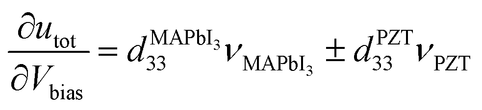 | (15) |
 was extracted for the region that is in-phase with the piezo-response of bare PZT and 4.2 ± 0.2 pm V−1 for the out-of-phase region.310
| Di = dijk = Xjk | (16) |
| xij = dijEk = dtijkEk | (17) |
 | ||
| Fig. 7 Piezoelectricity. Reproduced with permission.319 Copyright 2013, Springer Science + Business Media Dordrecht. | ||
Furthermore, a simpler molecular model used to explain the piezoelectric effect is shown in Fig. 8, which is the production of an electric charge because of the application of force on a material. Moreover, the centers of the positive and negative charges of every molecule happen together prior to subjecting the material to an external stress, resulting in an electrically neutral molecule, as illustrated in Fig. 8a. Conversely, in the presence of external mechanical stress, the internal reticular can be distorted, thus raising the division of the positive and negative centers of the molecule and producing little dipoles, as shown in Fig. 8b. Consequently, the opposite facing poles within the material revoke each other and fixed charges emerge on the surface, as demonstrated in Fig. 8c. This effect in the material which is polarized is said to be the direct piezoelectric effect and produces an electric field engaged to change the mechanical energy engaged in the distortion of the material into electrical energy. Although halide perovskites have not been reported to exhibit the reverse piezoelectric effect, several materials demonstrate the reverse piezoelectric effect.
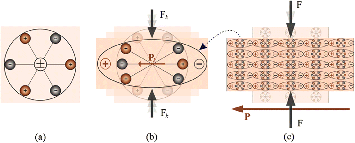 | ||
| Fig. 8 Schematic of simple molecular model of the piezoelectric effect. Reproduced with permission.319 Copyright 2013, Springer Science + Business Media Dordrecht. (a) Unperturbed molecule with no piezoelectric polarization. (b) Perturbed molecule exposed to an external force (Fk) and (c) polarization effect. | ||
4.4 New pyroelectric properties
Similar to ferroelectric and piezoelectric properties, it is crucial to consider pyro-electricity to understand the electronic properties and related applications of halide perovskites. Furthermore, pyro-electricity is an important property to express the crystallographic character of a material without an external field. Accordingly, MAPbI3 has a noncentrosymmetric structure and polar, which will hopefully put a closing stage to the uncertainty about the space-group of tetragonal halide perovskites, which is I4cm rather than I4/mcm. Moreover, understanding whether this symmetry is impressive and special to MAPbI3 or universal to its derivative tetragonal symmetries is interesting. The latest information on the lack of SHG in MAPbI3320 confirmed the rationale of the uncertainties though this query regarding the symmetry, which was verified by the existence of pyroelectricity, as well as showing the obvious proof for SHG as well as giving details of why no SHG was presented in ref. 320.Recently, motivating research outputs have been reported, as shown in Fig. 9A, in which a clear pyroelectric response, Jpyro, in the direction of 〈001〉 is observed.321 Furthermore, the direct proportionality between the conductivity and thermoelectricity of a semiconductor verifies that thermoelectric currents will further dominate at elevated temperatures due to the increase in its conductivity with temperature. Although at RT the pyroelectric response still exists, it is greatly small at a low temperature, where it becomes the controlling element of the thermally stimulated electric response (TSER). Despite the decrease in thermoelectricity, inferior electrical conductivity also should usually increase the effective spontaneous polarization and decrease the leakage currents, which should enlarge the pyroelectric response. Likewise, Fig. 9B shows further proof for the pyroelectric character of MAPbI3 derived from the reliance of the peak-current value on temperature. Moreover, the local maximum near the phase transition temperature (TC) at 330 K reveals an increase in the pyroelectric response as anticipated in the theory discussed elsewhere322 at a ferroelectric to paraelectric phase transition. As a result, the local extreme around TC is a physically powerful sign that tetragonal MAPbI3 is ferroelectric.323 Determining the imaginary (εim) and real (εre) relative permittivity with respect to temperature demonstrates a dielectric irregularity around TC (Fig. 9C), as formerly examined in MAPbI3 films,324 which supports the conclusion that tetragonal MAPbI3 is ferroelectric.325 The fading and regeneration of the pyroelectric response beyond the TC provide additional evidence of the non-polar character of the cubic phase and the polar nature of tetragonal MAPbI3, which agrees with the results for MAPbBr3.326
 | ||
| Fig. 9 Relative permittivity and pyroelectric response measurements. (a) Pyroelectric response, Jpyro, in the direction of 〈001〉, (b) the pyroelectric character of MAPbI3 derived from the peak-current value reliance on temperature. Reproduced with permission.321 Copyright 2011, Macmillan Publishers Limited. | ||
 | (18) |
| Di = ΔPs,i = piΔT | (19) |
Recently, synergistic photoexcited and photovoltaic pyroelectricity has been reported as an efficient method for guiding the charge carrier behavior of electronic and optoelectronic applications.328–330 This synergy of two effects is caused by the light–matter interaction. During light matter interaction, polarization of an electric field causes a stable photovoltaic current, while thermal redistribution results in an instantaneous pyroelectric current. This coupling of unique physical properties and spontaneous polarization makes halide perovskites such as (NPA)2(EA)2Pb3Br10 (NPA = neopentylamine and EA = ethylamine) possible candidates for research on the light-induced pyroelectric effect. These properties of halide perovskites are useful to develop light-induced pyroelectric effect-based self-powered X-ray devices that are better than heterojunction-based self-powered devices. Thus, halide perovskites are not only useful in photovoltaic and electronic devices but also in novel self-powered X-ray optoelectronic devices. These novel self-powered X-ray optoelectronic devices are based on the energy harvesting property of halide perovskites. Moreover, this alignment of coupling photovoltaic and pyroelectric properties gives an enhanced open-circuit voltage and transient short-circuit current, boosting the device performance.331
As shown in Fig. 10, recently, it was possible to develop the device architecture (Fig. 10a), working mechanisms (Fig. 10b) and enhanced self-powered ZnO/perovskite hetero-structured performances via the pyroelectric effect (Fig. 10c–e). During ultraviolet illumination, the polarization-induced pyroelectric effect is generated owing to non-central symmetric crystal structures. This pyroelectric effect is produced owing to the increase in temperature during ultraviolet illumination of the sample. This pyroelectric effect present at the interface facilitates charge transfer and reduces the possibility of charge recombination, enhancing the open-circuit voltage and transient short-circuit current.331Fig. 10c and d show the presence of the pyroelectric effect and photovoltaic effect together at some stage, where there are temperature gradients but the pyroelectric effect disappeared at the stage where the temperature became constant. The power conversion efficiency of halide perovskites is the result of the synergistic effect of both pyroelectric and photoelectric effects, together boosting the efficiency under light illumination. This is a good opportunity for halide perovskites to have wide energy harvesting and photo-sensing applications including nano-sensing. Similarly, this photo-pyroelectric effect has been observed in N-isopropylbenzylaminium trifluoroacetate (N-IBATFA).332 Furthermore, for better understanding the result, specific detectivity, D*, was measured, as shown in Fig. 10e. In all cases, the pyroelectric effect is responsible for both the photoresponsivity and detectivity, where D* = R(2e·Idark/S)0.5.331 It should be noted that R = (Ilight − Idark)/Pill, where Pill = Iill × S. S is the effective area of the photodetector, R is the corresponding photoresponsivity, Pill is the illumination power and Iill is the short circuit current with illumination.
 | ||
| Fig. 10 Schematic demonstration of the structure, mechanisms and pyroelectric effect induced by self-powered ZPH PDs. Reproduced with permission.331 (a) Device architecture, (b) working mechanisms, (c) self-powered ZnO/perovskite hetero-structured performances, (d) photovoltaic effect and (e) specific detectivity, D*. Copyright 2015 Macmillan Publishers Limited. | ||
 | ||
| Scheme 6 Halide perovskite crystal symmetry showing ferroelectricity, piezoelectricity and pyroelectricity effects. | ||
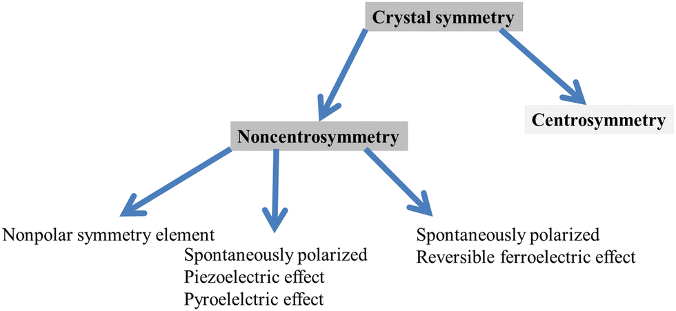
For instance, if a physical characteristic is linked to a symmetry element of a material, this characteristic should not alter its value.271 Rather, it pursues from Neumann's principle that a number of characteristics, for example, pyroelectricity and piezoelectricity, can be presented merely in materials with sure symmetries and that other properties for instance elastic compliance, electrostriction and dielectric permittivity are present in all materials. Furthermore, the symmetry requirements can considerably decrease the number of independent and nonzero elements of a property tensor. Moreover, the piezoelectric and other effects explained via odd-rank tensors are not allowed through the symmetry in crystals that belong to the 432 noncentrosymmetric point group and eleven centrosymmetric groups. Accordingly, crystals that belong to the remaining twenty noncentrosymmetric groups from the total thirty two point groups can show the piezoelectric effect and occasionally called piezoelectric point groups, among which ten of the piezoelectric point groups show and own a unique polar axis without a spontaneous polarization vector, Ps, in the presence of the pyroelectric effect present and an external electric field.
 | ||
| Fig. 11 Process of strain formation. The positive thermal expansion coefficient (A–B), intensity vs. temperature (C–D). Reproduced with permission.56 Copyright 2017, American Association for the Advancement of Science. | ||
As shown in Fig. 12, mixed halide perovskites such as (FAPbI3)0.85(MAPbBr3)0.15 have inhomogeneity, resulting in strain properties.333 Not only these mixed perovskites but also MAPbI3 has inhomogeneity.334 This inhomogeneity is believed to be the source of strain in halide perovskites. The tensile strain was observed to decrease on reversing the heat treatment procedure (Fig. 12a and b). This indicates that the homogeneity of the lattice structure is small at smaller strain. Furthermore, compressive strain was observed in the as-synthesized perovskite film, indicating that the solvent left pinholes after annealing given that it was not distributed smoothly during the annealing process (Fig. 12c and d). This caused trap-assisted recombination, as shown in Fig. 12d. Thus, the power conversion efficiency was observed with or without tensile strain, and strain free and compressive strain are shown in Fig. 12e and f. These strains were caused by the temperature gradients during the preparation of the films.
 | ||
| Fig. 12 The presence of Strain study in (FAPbI3)0.85(MAPbBr3)0.15. (a) Intensity vs. 2Theta for strain free sample, (b) 2Theta vs. sin2 function for strain free sample, (c) intensity vs. 2Theta for compressed strain, (d) 2Theta vs. sin2 function for compressed strain film, (e) Tensile strain vs. strain free, (f) current density vs. voltage for tensile strained and strain free film. Reproduced with permission.333 Copy right 2019, Nature publishing group. | ||
The presence of strain and gradient distribution in the film resulted in structure inhomogeneity, serving as recombination centers, and thereby reducing the charge transfer and device efficiency. This suggests that energy harvesting devices can be fabricated via strain engineering such as memory and sensors devices, particularly electronic devices, for instance, nonvolatile memory,335,336 tunable capacitors,337 solar cells,329 and tunnel junctions.338 Furthermore, there are two approaches to the increase piezoelectric energy harvesting to generate power, i.e., increasing the strain via applied stress and coupling mode. This coupling mode depends on the applied force and material poling directions.
4.5 Thermoelectric properties
Thermoelectric materials are essential for thermoelectric applications. For this purpose, halide perovskites have recently been reported as thermoelectric materials.339–348 An outstanding thermoelectric performance is expected from n-type semiconductors, and thus Cs(Ge,Sn)I3 becomes a possible alternative material.340 Its Seebeck coefficient increases as its band gap increases. This makes it suitable for thermoelectric applications. Moreover, CsSnBr3 is an additional thermoelectric property recently reported with promising results.339 Its ZT value was maximized at ∼0.01 and its promise indicates that its thermoelectric performance can increase via doping engineering.339,349,350 It was observed that photoexcitation is an effective way to enhance the electrical conductivity and Seebeck coefficient through excited states in CH3NH3PbI3.351 Cs3Cu2I5 has also been reported as a candidate thermoelectric material for possible thermoelectric applications.352 The results indicated that this material is a possible n-type candidate material, corresponding to a thermodynamic heat-to-electricity power conversion efficiency of 15% and a thermoelectric figure-of-merit ZT of 2.6.352 The thermoelectric figure-of-merit ZT is given by ZT = σS2T = PT/k, where P(=σS2) is the thermoelectric power factor, k is the thermal conductivity, T is temperature, σ is the electrical conductivity and S is the Seebeck coefficient (a measure of the thermoelectric property). Thermoelectric materials with superior Seebeck coefficient are adaptable and vigorous for waste-heat recovery. Both electrical conductivity and Seebeck coefficient are dependent on the carrier concentration, charge carrier mobility, temperature, relaxation time, average band effective mass, Fermi–Dirac distribution function and density of state. For a material to have multiferroicity, ferroelectricity or piezoelectricity, it has to possess non-centrosymmetry, but for it to be thermoelectric it is not constrained by symmetry.353 It must be known that the merit of thermoelectric conversion requires high electrical conductivity (s) and low thermal conductivity (k). This requirement makes thermoelectric materials difficult to engineer.Even if promising research work has been done in the field of halide perovskites, much work still needs to be performed. It necessary to conduct research to make halide perovskites suitable for thermoelectric applications. Essential parameters such as Hall coefficient, thermal conductivity, electrical resistivity, charge carrier concentration, Seebeck coefficient and mobility should be discovered for a better understanding of the thermoelectric properties and applications of halide perovskites. The application of thermoelectric materials is cooling such as in optoelectronics, small-scale refrigeration, detectors and power generation such as in deep space missions has been reported.354 Halide perovskites should be tested whether they can succeed in these potential thermoelectric applications with a deep understanding.
From a thermodynamic approach, understanding and considering the coupling mechanisms among the electrical, thermal and elastic parameters and their synergistic effects on the performance of halide perovskites will be vital for future development. The outcomes are equations of state, which present relationships among the material parameters computed under different experimental conditions and the coupling mechanism is via the thermodynamic approach. These relationships are necessary for understanding and modeling the response of ferroelectric, ferroelastic, pyroelectric and piezoelectric devices. Moreover, the coupling thermodynamic approach is presented in the following discussion and broadly in the literature.273,355,356 According to the first and second laws of thermodynamics, the reversible change dU in the internal energy U of an elastic dielectric subjected to a small change in entropy dS, strain dx and electric displacement dD is shown in eqn (20).
| dU = TdS + Xijdxij + EidDi | (20) |
| G = U − TS −Xij − EiDi | (21) |
| dG = −SdT − xijdXij − DidEi | (22) |
 | (23) |
 | (24) |
 | (25) |
 | (26) |
Each partial derivative in eqn (24) and (25) recognizes a physical effect,271 as specified in the equations. Because the order wherein the derivatives are used is irrelevant,356 it follows eqn (22), (24) and (25) that, for example,
 | (27) |
Eqn (8) shows the thermodynamic equivalence of the converse and direct piezoelectric effect. Equally, it can be revealed that this is thermodynamically comparable to the pyroelectric effect (∂Di = ∂T)X,E, electrocaloric effect (∂Si = ∂Ei)T,X, piezocaloric effect (∂S = ∂Xij)T,E, and thermal expansion (∂xij = ∂T)X,E. All these thermal, electrical and elastic effects are related to each other and represented by the general scheme shown in Scheme 7.
 | ||
| Scheme 7 Representation of the general relationships among mechanical and electrical domain and dielectric and elastic behaviors observed in ferroelectric materials. Reproduced with permission.357 Copyright 2004, Oxford University Press. | ||
5. Nanometer-scale domain characterization
From the perspective of advanced materials characterization at the nanoscale, developing and establishing nanometer-scale domain characterization in line with materials development is the first step unless materials properties become challenging to understand at the end because of the limit or lack of sensitive techniques with high detection limit and resolution. Moreover, to understand the origin and mechanisms of strain switching, compressive and tensile stress at the nanoscale, absence or presence of an inversion center, noncentrosymmetric and centrosymmetric properties, polarization switching, domain formation mechanisms, and polar order at the surface, interface and wall, nanoscale structural characterization is necessary because of the many controversies regarding the presence or absence of ferroelectricity in MAPbI3.358 Therefore, it is necessary to organize nanoscale and advanced characterization tools for the successful understanding of halide perovskites such as atomic force microscopy (AFM), piezoelectric force microscopy (PFM), photothermal induced resonance (PTIR), photoinduced force microscopy (PiFM), nonlinear optical spectroscopy, and second harmonic generation (SHG) and theoretical or computational methods such as first principles calculations, as discussed in detail in this section and summarized in Scheme 8. | ||
| Scheme 8 Representation of perovskite characterization methods and approaches. | ||
5.1 First-principles calculations
In parallel to the experimental perspectives, considering and understanding the theoretical perspectives and principles have vital contributions in designing and modeling new materials, and predicting their properties based on their functionalities. Progress in realizing ferroelectricity, piezoelectricity and pyroelectricity requires contributions from first-principles. Furthermore, there are very important concepts that first-principles studies can demonstrate, as follows: (1) the importance of hybridization. Contrasting the respected Slater rattling ion model,359 the main element in oxide ferroelectrics is covalence or hybridization between the cation and its oxygen neighbors, which lets the cation to travel off-center. Presently, this idea is extensively applied in experiments, and thus for the improvement of novel piezoelectric materials, it should be borrowed in the halide perovskite field. (2) The idea of polarization rotation, which is accountable for the huge electromechanical coupling seen in relaxor ferroelectrics such as Pb(Mg1/3,Nb2/3)O6 (PMN)-PbTiO3 (PT).360 (3) The association between cation ordering and polar nanoregions in relaxors.361,362 (4) The determination of a morphotropic phase boundary in pure PT at high pressures with vast electromechanical coupling in the transition region.363 (5) The discovery of reentrant ferroelectricity, with ferro-electricity regenerating at extremely high pressures, representing an option for entire novel classes of ferroelectric materials.364 Likewise, there are essential and more advanced concepts that should be addressed in hybrid perovskites using this method, as follows: (a) determining the role of large effective charges in electromechanical coupling, (b) understanding the function of hybridization and covalence in ferroelectric instability, (c) understanding the function of polarization rotation in single-crystal relaxor ferroelectrics, (d) the idea of polar ferroelectric superlattices, (e) primary understanding of macroscopic polarization, (f) planning paths for novel materials, and (g) understanding of the necessity for materials to be multiferroics. Therefore, the movement and ordering of organic cations in halide perovskites are both still controversial theoretically.365,366Therefore, from the current theoretical perspective, the polarization intensity donated from the organic cations becomes predominantly controversial. For instance, Walsh et al. reported the spontaneous formation of ferroelectric domains in MAPbI3 and a huge polarization value of 38 μC cm−2 was demonstrated. Another study showed that the MA cations in tetragonal MAPbI3 have a special position along the c axis, and the polarization intensity was approximated to be 4.42 μC cm−2, which is mostly denoted by the MA dipole.366 The authors also clarified that the large inconsistency with Walsh's study was perhaps because of the absence of relaxation or the possible inclusion of polarization quanta. According to other research groups, the bulk polarization involvement solely from the organic molecular dipole moment is less than 2.5 μC cm−2, and the PbI3 inorganic lattice has the main contribution to the polarization.365 Furthermore, their calculations demonstrated that the anti-ferroelectric tetragonal structure with almost zero net polarization is more stable than its ferroelectric counterpart by 21 meV, indicating that ferroelectric domains cannot form spontaneously at room-temperature. Conversely, the electronic structure was calculated using first-principles to disclose a ferroelectric tetragonal structure with a polarization of about 8 μC cm−2 contributed by the organic cations.206
5.2 Atomic force microscopy
To investigate the microscopic origin of ferroelectric, piezoelectric and pyroelectric properties, AFM can associate the topography of a sample with other local material electrical characteristics, such as conductivity and electrical potential.199,200,367,368 This technique has been instrumental in ushering in the age of nanotechnology owing to its high resolution and sensitivity across a range of interaction forces, allowing AFM to find applications in materials science, physics, chemistry, and biology.369 Initially developed to map the surface topography of materials,370 various modalities were subsequently developed to probe mechanical, magnetic, electrical, and chemical properties.371–3785.3 Photo-induced force microscope
This technique is still in its infancy, although early models can already extract quantitative information from PiFM images.379,380 It is based on photoinduced forces between the sample and a sharp tip. A diagram of the interaction between the tip and the (nano)particle is shown in Fig. 13a, in which the system is lit via an inward light field, E0. The condition in the tip-sample junction can be illustrated by estimating both the sample particle and the tip apex as polarizable spheres and considering only dipolar interactions. | ||
| Fig. 13 Photoinduced interaction and configuration of PiFM. Reproduced with permission.381 Copyright 2015, the American Chemical Society. (a) Representation of the interaction between the photoinduced tip dipole in the focal plane of a tightly focused field and in the target particle. (b) Configuration of the PiFM. | ||
Fig. 13b shows an inverted optical microscope, which applies an AFM detection head in place of a photodetector. The primary signal in PiFM is the time-integrated, photoinduced force, as registered by the AFM head rather than detecting optical radiation. Furthermore, the light source in the PiFM system is a laser, which can either be a continuous wave (cw) or pulsed laser, depending on the type of optical experiment.
5.4 Visualizing nanometer-scale domain patterns
PFM is an instrument used to set up polarization switching by visualizing nanometer-scale domain patterns15,44,93,382 as well as nanoscale piezoelectricity and ferroelectricity. Recently, the properties of 1D piezoelectric nanostructures have been investigated using PFM.383 This is an effective technique for drawing the topography and conducting nondestructive property characterization of piezoelectric and ferroelectric materials at the nanoscale, giving convincing evidence of the switching behavior and domain structures in single-crystal and polycrystalline MAPbI3. Nevertheless, it is recognized as being sensitive to the surface charge and ionic properties384 because it is applied in electrochemical force microscopy.385–387 Similarly, the surface topography leads to strong topographic cross-talk,388,389 which can give rise to the recognition of step edges as ferroelectric domains or ferroelastic domains.390 Thus, the surfaces of these materials are particularly unstable in the ambient environment, seriously leading to the formation of secondary phases such as PbI2, which can further mask their intrinsic characters.391,392 Similarly, it is possible that PFM is an AFM method based on the inverse piezoelectric effect, which locally probes piezoelectric samples and visualize ferroic domains.200,3685.5 Photothermal-induced resonance
This technique computes the transient thermal expansion caused as a result of light absorption by a sample via a contact-mode AFM tip. It is also a composition-sensitive scanning probe technique, which combines the lateral resolution of AFM with the chemical accuracy of absorption spectroscopy.206,393,394 To better illuminate the samples, they are lit from the underneath in an entire internal reflection design to reduce the interaction of light with the AFM tip, as shown in Fig. 14a. Additionally, the absorption of a laser pulse in the sample results in sample expansion, excitation of the AFM cantilever motion, and local heating, which is controlled by shinnying the AFM laser beam from the cantilever onto a four-quadrant photodetector (Fig. 14a). Moreover, the ability to quantify the chemical composition395,396 with a spatial resolution down to 20 nm394 has made this technique very popular for analyzing thin organic397–399 and metal–organic materials.396,400,401 However, because the PTIR signal is also proportional to the sample linear expansion coefficient, inorganic samples are typically challenging to measure. Furthermore, the thermal expansion is very rapid compared to the AFM response. It is sufficient to stimulate a number of the smallest-frequency mechanical modes of the cantilever (Fig. 14c). The recurrence frequency of the laser pulses is sufficient to let the cantilever finish the ring down (Fig. 14b) prior to the appearance of the latest pulse. Prominently, the PTIR signal is related to the energy absorbed,176 and openly as good as with FT-IR spectral libraries,402,403 enabling the identification of materials. | ||
| Fig. 14 Instrumentation: reproduced with permission.404 Copyright 2013, the American Chemical Society. (a) Picture of the PTIR technique, (b) high peak to peak deflection and (c) amplitude of different contact resonance modes. | ||
5.6 Differentiating noncentrosymmetric and centrosymmetric crystals
Nonlinear optical spectroscopy is important to analyze films, which is an efficient and simple tool to differentiate between noncentrosymmetric and centrosymmetric crystals, indicating the polar or nonpolar character of the crystal structure.5.7 Identification of inversion center and non-centrosymmetry
Second-harmonic generation (SHG) is a nonlinear optical technique developed to confirm the absence or presence of an inversion center in crystals.405,406 Given that only non-centrosymmetric materials are SHG-active because of their non-zero hyperpolarizability, β, it is also a sensitive tool for probing the loss of inversion symmetry in a phase transition. Furthermore, the molecular bottleneck for competent SHG functions is determined by the necessity of insignificant absorption in the spectral region of attention and large first-order molecular hyperpolarizability (β).407 Although wide-ranging research has sketched a variety of issues for approximating β,408–411 the main building blocks for the development of this technique is the translation of molecular non-linearity into a limited macroscopic second-order susceptibility (χ(2)), which demands crystallization into a non-centrosymmetric lattice. The total SHG intensity (I2ω) emitted by a sample is calculated using the Kurtz–Perry method,412 as shown in eqn (28) as follows: | (28) |
5.8 Identification of the polar crystallographic orientation
For the investigation of a polar dielectric crystal, identification of the polar crystallographic orientation is required. Following powder X-ray diffraction of pulverized crystals, which confirms that the grown crystals are MAPbI3, it is possible to determine the polar direction of the crystals using specular diffraction from the surface of a single crystal.6. New application trends beyond photovoltaics
Piezoelectric energy harvesting devices are great solutions for a given application that requires high energy density, high voltage, little mechanical damping and high capacitance.413 For this purpose, halide perovskites have been tested as new energy harvesting piezoelectric materials.15 Presently, their wide range of energy harvesting applications beyond photovoltaics has become a hot topic with great attention from the scientific community.414 In this section, we present piezoelectric energy harvesting, electromechanical and electronic energy conversion and storage device applications beyond photovoltaics, light emitting diodes and laser applications, which are useful to the scientific community.Halide perovskite materials are widely researched for various applications such as photovoltaics, lasers, light emitting diodes, and photocatalysis. However, recently, these materials have become essential materials for energy harvesting applications such as self-powered units, wireless electronics, and storage devices, as shown in Table 2.
| Energy harvesting materials | Output voltage/V | Output current density | Current | Specific capacity | d 33 | Ref. |
|---|---|---|---|---|---|---|
| EDABCO = (N-ethyl-1,4-diazoniabicyclo[2.2.2]octonium), PVDF = polyvinylidene fluoride. | ||||||
| 4Cl-MAPbI3 PENG | 5.9 | ∼0.61 μA cm−2 | 104 | |||
| CsPbCl3 | 257 | 3.04 W m−2 | 27.87 μA | 415 | ||
| FASnI3:PVDF | 23 | 35.05 mW cm−2 | 73 pm V−1 | 99 | ||
| FASnBr3 | 94.5945 Vp-p | 18.95 μW cm−2 | 19.1 μAp-p | 5050 pm V−1 | 101 | |
| MA2SnCl6 | 7.33 μW cm−2 | 589.98 mA h g−1 | 100 | |||
| Cs2NaBiCl6 | Stable 300 mA h g−1 | 416 | ||||
| TMCM2SnCl6 | 81 | 0.6 kV cm−1 | 2 μA | 137 pC N−1 | 241 | |
| CH3NH3PbBr3 | 175.5 mA h g−1 | 417 | ||||
| CH3NH3PbI3 | 2.7 | 140 nA cm−2 | 43.6 mA h g−1 | 5.12 pm V−1 | 417 | |
| CH3NH3PbBr3:3Li+ | 200 mA h g−1 | 418 | ||||
| CsPb2Br5 | 200 | 45 mW | 2.8 | 72 pm V−1 | 419 | |
| Poled CH3NH3PbI3 | 2.7 | 140 nA cm−2 | 15 | |||
| Li4Ti5O12 | 175.5 mA h g−1 | 420 | ||||
| BaTiO3 | 6.5 | 70 nA cm−2 | 419 | |||
| EDABCO-CuCl4@PVDF | 63 | 43 μW cm−2 | 2.1 μA cm−2 | 165 pm V−1 | 281 | |
6.1 Electrical properties and corresponding applications
From the perspective of harvesting energy, it is crucial to test halide perovskites for their electronic functionalities beyond photovoltaic, photonic and optical applications. In the realization of these applications, the external stimuli that produce the corresponding application should also be considered. For instance, when a certain type of perovskite photovoltaic device is exposed to external stimuli such as light and thermal energy, the related processes are similar for different applications. In this case, to avoid presenting a generalized concept, we discuss the properties and applications421 of several vital phase mixed-metal oxide-based perovskites, as shown in Table 3. The importance of these materials is in accordance with their intrinsic ferroelectric, piezoelectric, pyroelectric and dielectric properties of significance in relation to electronic applications such as field effect transistors, capacitors, transducers, high-k dielectrics, logic circuitry, actuators, dynamic random access memory, and electromechanical devices.422–424 It is an excellent opportunity and great assignment for the scientific community to check whether halide perovskite materials can be used as alternative materials for the electronic applications described in the Table 2. Above all, it will be of great interest to determine whether halide perovskite materials really possess all the electronics properties stated in the Table 3.| Materials | Properties | Applications |
|---|---|---|
| Note.a Indicates the proposed semiconducting properties and the corresponding applications are ‘not yet reported,’ which need future investigations. | ||
| (Ba,Sr)TiO3 | Pyroelectric | Pyrodetector |
| BaTiO3 | Dielectric | Capacitor, sensor |
| PbTiO3 | Piezoelectric pyroelectric | Acoustic transducer pyrodetector, |
| Pb(Zr,Ti)O3 | Pyroelectric | Pyrodetector |
| Piezoelectric | Surface acoustic wave device, substrate | |
| Dielectric | Nonvolatile memory, | |
| Electro-optic | Waveguide device | |
| (Pb,La)(Zr,Ti)O3 | Electro-optic pyroelectric | Waveguide device, optical memory display pyrodetector |
| (LiNbO3/Ti) | Electro-optic | Waveguide device, second harmonic generation, optical modulator |
| LiNbO3 | Piezoelectric | Pyrodetector, surface acoustic wave device |
| K(Ta,Nb)O3 | Electro-optic pyroelectric | Waveguide device, frequency doubler pyrodetector |
| Pb(Mg1/3Nb2/3)O3 | Dielectric | Memory, capacitor |
| FAPbBr3 | Piezoelectric | Piezoelectric nanogenerator |
| Pyroelectric | Acoustic transducera, pyrodetectora | |
| Electro-opticsa | Waveguide devicea, second harmonic generation? optical modulators? | |
| MAPbI3 | Piezoelectric, pyroelectric, electro-opticsa | Piezoelectric energy harvesting devices, acoustic transducera, pyrodetectora |
| Waveguide devicea, second harmonic generationa, optical modulatorsa | ||
| CsPbX3 | Piezoelectrica | Piezoelectric energy harvesting devicesa, acoustic transducera, pyrodetectora |
| Pyroelectrica | Waveguide devicea, second harmonic generationa, optical modulatorsa | |
| Electro-opticsa | ||
As shown in Fig. 15a, the dielectric constant of CH3NH3PbI3 and Cl-MAPbI3 was studied and found to be dependent on frequency.104 The dielectric constant for CH3NH3PbI3 was ∼43 at 100 kHz. To understand the property of the dielectric constant, various amounts of Cl were added and ∼90.9 was found for the 4Cl-MAPbI3 sample but ∼62 for the 10Cl-MAPbI3 sample. This indicates that there should be an optimum amount of Cl to obtain the optimum dielectric constant value. Moreover, the value of the dissipation factor (D) for both CH3NH3PbI3 and Cl-MAPbI3 is shown in Fig. 15b, which indicates that D increased with an increase in the amount of Cl. Furthermore, Fig. 15c shows the dissipation factor and dielectric constant at 100 kHz as a function of the amount of MACl and MAI. The dense and smooth morphology of the sample film is suggested as the possible cause for the larger dielectric constant obtained for the Cl-incorporated MAPbI3. An experiment was performed to further understand the effect of an increasing amount of Br, where the dielectric constant increased gradually. The 6Br-MAPbI3 sample achieved a value of ∼71.6 at 100 kHz. As shown in Fig. 15d and e, a lower dissipation factor was observed owing to the incorporation of Br, which resulted in the formation of dense perovskite films. This incorporation of Cl and Br induced a strain effect for piezoelectric energy harvesting and effective power generation. Based on this concept, compressive strain was created, generating an output voltage of ∼0.78 V and output current density of ∼0.11 μA cm−2 from CH3NH3PbI3 and output voltage of 2.75 V from the 4Cl-MAPbI3 mixed perovskite. The larger current density observed in Fig. 15g shows that the incorporation of the halide resulted in the formation of denser and smoother surface morphologies. The P–E hysteresis loop is shown in Fig. 15h and 0.56 μC cm−2 was obtained for 4Cl-MAPbI3. The increased polarization and dielectric constant is owing to the interfacial polarization caused by the coexistence of two phases such as MAPbCl3 and MAPbI3.14,427 The high leakage of the current density and larger dielectric constant properties demonstrated by each sample are useful for high energy harvesting applications.
 | ||
| Fig. 15 Dielectric study of the mixed halide-MAPbI3 films: Dielectric constant vs. frequency (a), dissipation factor vs. frequency (b), dielectric constant vs. weight ratio (c) for MAPbI3, and dielectric constant vs. frequency (d), dissipation factor vs. frequency (e), dielectric constant vs. weight ratio (f), for Br-incorporated MAPbI3, as well as leakage current density vs. electric field (g) and polarization vs. electric field (h). Reproduced with permission.103 Copyright 2020, American Chemical Society. | ||
6.2 Structure preference of halide perovskite nanogenerators
From the perspective of device architecture or structure, understanding and developing the suitable hybrid perovskite nanogenerator device architecture to satisfy the triple ‘E’ rule of efficient, economical and environmentally friendly is a current and burning issue for the scientific community. There are reports on perovskite nanogenerators demonstrating that halide perovskites are promising energy harvesters for nanogenerator applications.100,427 In recent times, periodically release operations and vertical compression in the course of the piezoelectric structure have been reported, as shown in Fig. 16.14 Moreover, halide-controlled perovskite-based nanogenerators and capacitors have been reported.104,415 The reasons for the high-density powered nanogenerators are suggested to be their charging polarities,414 soft elastic nature and soft polar optic phonons.99 The operation of a nanogenerator is via two ways, as shown in Fig. 16a, where once the electric dipoles are aligned in a single direction when vertical compression is applied to the nanogenerator, the piezoelectric potential causes electrons to move from the top electrode to the bottom electrode through an external circuit. The other way, as demonstrated in Fig. 16b, is that the piezoelectric potential inside the device directly disappears when the compressive strain is removed and the collected electrons from the bottom electrode flow back to the top electrode and an electric signal is shown in the reverse direction. The aim here is not just to explain the operation but to highlight the important concepts that motivate researchers to investigate how to realize nanogenerators made of halide perovskites that satisfy the triple ‘E’ regulations. | ||
| Fig. 16 Hybrid perovskite piezoelectric nanogenerator structure. (a) Electrons move from the top electrode to the bottom electrode side (b) collected electrons from the bottom electrode flow back to the top electrode. Reproduced with permission.14 Copyright 2016, WILEY-VCH Verlag GmbH & Co. KGaA, Weinheim. | ||
More importantly, the concern of how to produce electrical energy from mechanical vibration is also a challenging lesson. Among these concerns, considering that the beam structure is the most frequent solution to obtain electrical energy from mechanical vibrations has a vital contribution. Accordingly, considering the main factors such as generator structure, generator size, electronic system of the control and storage of energy, and piezoelectric material during the generation of effective electric energy using piezoelectric generators has great importance. The most often tested piezoelectric generator structures are designs in which the basic element, apart from the piezoelectric actuator, is the cantilever beam. One can single out a few possibilities of the connection of piezoelectric materials to the beam, as follows:
1. A beam made of the base material, with no piezoelectric properties, on which there is one (unimorph) or two piezoelectric material layers (bimorph). A generator with two plates of PZT ceramics (bimorph) is presented in Fig. 17a.
 | ||
| Fig. 17 Various alternative cantilever beams as the structure base of a piezoelectric generator. Reproduced with permission.428 Copyright 2013, Pomiary Automatyka Robotyka. | ||
2. Beam with an additional element influencing the increase in stress in the piezoelectric material layers. An example of a generator with one piezoelectric layer and an additional element is presented in Fig. 17b.
3. A beam without piezoelectric material layers with an additional setup containing a piezoelectric material. An example of a generator of this type is presented in Fig. 17c.
4. A beam with an additional element,429 making it possible to install more piezoelectric layers (Fig. 17d).
During beam bending, stresses appear in the piezoelectric material, on which electric charge builds up. An additional mass, M, is installed at the end of the beam to increase the stress in the piezoelectric layers. Considering the fact that generators can power wireless sensors, the generator structures should be small, i.e., about 1 cm3. It should be noted that in generator structures based on cantilever beams and PZT plates, the direction of external force action is perpendicular to the direction of polarization. Hence, the piezoelectric coupling is indicated by the coefficient k31.430 An increase in stress in the piezoelectric element can be acquired by various beam shapes, most often a rectangle but also a triangle,431 as well as by various geometry solutions of beam fixing to the object which is the source of vibration (Fig. 18).
 | ||
| Fig. 18 Cross-sections of the beam in generators. Reproduced with permission.432 Copyright 2010, Proceedings of PowerMEMS. | ||
From the perspective of coupling modes for easy operation in line with the device architecture perspective, at least two frequently utilized coupling modes for piezoelectric power generators should be considered, as recognized by the direction of the electric charge and mechanical force. Fig. 19a illustrates the ‘33’ mode, which indicates the charges accumulated on the electrode surface at right angles to the direction of polarization when compressive mechanical or tensile forces are applied in the axis of polarization. Similarly, Fig. 19b shows the ‘31’ mode, which indicates the charges accumulated on the electrode surface at right angles to the direction of polarization when a force is applied in the direction at right angles to the axis of polarization.433 For most piezoelectric materials, the coupling factor of the 33-mode, k33, is larger than the coupling factor of the 31-mode, k31, but this have has not been reported to date. In the 31-mode, the mechanical stresses are directed along the 1-axis. Stresses can be simply realized by bonding the piezoelectric element to a substructure experiencing bending, while the 33-mode energy conversion can attain a superior output power by increasing the layer of the ceramic (Stock type). For a very low-pressure source and limited size, the 31-mode conversion may be more beneficial for energy conversion.434 Because of the small size of the generator with limited environmental sources for mechanical energy, 31-mode energy conversion is appropriate for piezoelectric microgenerator applications in micro-electromechanical systems (MEMS).
 | ||
| Fig. 19 Important coupling modes for piezoelectric materials. Reproduced with permission.435 Copyright 2004, Institute of Physics Publishing (Smart Materials and Structures). (a) ‘33’ coupling mode and (b): ‘31’ coupling mode. | ||
6.3 Expected piezoelectric energy conversion from perovskite materials
According to the global direction and demand for energy conversion, there is great concern and need to achieve sufficient energy, and also extra or reserve energy. Another global concern is the development of semiconducting materials that can satisfy the global energy demand, in addition to the global concern of what type of device architecture or structure to satisfy the triple ‘E’ rule and operating conditions discussed in the previous sections. Therefore, it is a great issue and concern of how much energy can be globally achieved from energy harvesting semiconducting materials. To date, oxide-based perovskite piezoelectric materials, along with a number of energy conversion materials, are broadly applied as smart structures, which are generally categorized into two types depending on their energy conversion route, as follows:435 (1) sensor type, wherein an electric charge is generated when a mechanical stress is used and (2) actuator type, where the piezoelectric element experiences a variation in dimensions when an electric field is applied, by which electric energy is changed into mechanical energy derived from the indirect piezoelectric effect. The field of potential applications of piezoelectric generators in energy harvesting systems is marked by the range of electric power that they can generate. Based on published laboratory research results for piezoelectric generators, one can state that the generated power does not exceed several mW. The maximum power for selected piezoelectric generators and their dimensions are presented in Table 4.| Structure of piezoelectric generator | Piezoelectric material | Dimension of piezoelectric material [mm] | Dimension of generator [mm] | Frequency of source vibration [Hz] | Generated power [mW] |
|---|---|---|---|---|---|
| Cantilever beam | PZT | 4 × patches: 25.4 × 50.8 × 0.254 | 14.3 × 50.8 × 1.27 | 29.5 | 1.4 |
| Cantilever beam | MFC | 2 × patches: 85 × 28 × 0.3 | 114.3 × 50.8 × 1.27 | 29.7 | 1.7 |
| Connected four cantilever beams | PZT | 4 × patches: 30 × 10 × 0.5 | 200 × 200 × 0.2 | 35.5 | 8.0 |
| M-shaped beam | PZT | 2 × patches: 25 × 25.4 | 220 × 25.4 × 0.254 | 14.5 | 2.6 |
| Cantilever | FAPbBr3 | — | 1 × 3 | — | 32.3 × 10⁻³ |
According to the published research results, three general factors influence the energy conversion efficiency, including the greatest electric power is generated for a generator resonant frequency nearing the driving frequency of the vibration source and the value of electrical power depends on the strain of the piezoelectric material in the generator. Hence, generators with additional elements influencing the increase in strain generate more electrical power than the typical cantilever beam generator. Finally, the electrical power is proportional to the size of the piezoelectric material used in generators.439
The performance of FAPbBr3-PDMS nanogenerators is approximately 0.44%,440–443 as shown in Table 5. External compression cannot generate large strain on a piezoelectric FAPbBr3 nanoparticle because of the presence of the PDMS matrix, which bears the greater part of the compression.444 Nevertheless, the hybrid composite piezoelectric nanogenerator can successfully avert the cracking and breaking of the embedded piezoelectric nanoparticles under mechanical stress. Above all, piezoelectrics are smart for use in large-scale piezoelectric energy harvesting, owing to their low cost, mechanical robustness, and easy device fabrication.14
| Nanogenerator | Output voltage [V] | Output current | Efficiency |
|---|---|---|---|
| Note that the symbol ‘?’ indicates a research question that need further investigation for the future application of halide perovskites. | |||
| NaNbO3/PDMS | 3.20 | 16 nA cm−2 | — |
| LiNbO3/PDMS | 0.46 | 9.11 nA | — |
| BaTiO3/PDMS | 5.50 | 350 nA | — |
| ZnSnO3/PDMS | 9.70 | 0.9 μA cm−2 | — |
| PMN-PT/PDMS | 7.80 | 2.29 μA | — |
| FAPbBr3/PDMS | 8.50 | 3.4 μA cm−2 | 0.44% |
| MAPbX3/PDMS | ? | ? | ? |
| CsPbX3/PDMS | ? | ? | ? |
6.4 Constructing halide perovskite piezoelectric dampers
It is clear that the inspiring devices are constructed from important materials with inspiring semiconducting, electrical, optical and structural properties. Thus, to avoid a general discussion, we use PZT as an example of these important materials with inspiring properties for inspiring applications. One of the fascinating functions of PZT composites is the ability to construct a passive mechanical damper as a motivating concept related to the important question of how to construct inspiring piezoelectric dampers from halide perovskites? For instance, taking the capacitance of the piezoelectric material as C and the vibration frequency as f with the series resistance as R, damping happens very quickly when the series resistor is chosen when the impedance corresponding condition, R = 1/(2πfC), is fulfilled.449 When a composite of piezoceramic powder, carbon black and polymer was fabricated (Fig. 20a), the electrical conductivity of the composite was significantly altered by the addition of small amounts of carbon black (i.e., percolation effect).450 A very interesting question to the halide perovskite community is how do these piezoelectric dampers benefit from these low cost materials and are simple to fabricate? However, halide perovskite materials have not been tested thus far for this purpose, although they were recently reported as materials that fulfill piezoelectric properties. | ||
| Fig. 20 Damping and modes of energy harvesting. Reproduced with permission.450 Copyright 1991, IOP Publishing. (a) Representation of vibration damping. Frequent models of piezoelectric energy harvesting devices: (b) piezoelectric 33-mode and (c) piezoelectric 31-mode. | ||
6.5 Constructing halide perovskite piezoelectric energy harvesters
Wearable electronic devices451 and wireless intelligent sensor networks452 have recently developed quickly in areas such as medical science, energy, roads, bridges and military affairs. However, an essential issue that needs to be considered is the energy delivered by these devices. Chemical batteries show a number of drawbacks, for example, large volume, inability to integrate with MEMS devices and short storage time with respect to the main energy. Also, their installation positions are not suitable for their replacement in numerous sensors. Consequently, piezoelectric energy harvesters that can acquire energy from the vibration environment are now a hot research topic based on the concern of an energy substitute for chemical batteries.453–455 Moreover, the advantages of piezoelectric energy harvesters include easy miniaturization, simple structure, no pollution, no electromagnetic interference and no heat to meet the energy needs of low-power consumption products. As a result, they are becoming vital choices.For the construction halide perovskite piezoelectric energy harvesters, it is crucial to consider influencing parameters such as resonance voltage, structure type and resonance frequency, in addition to the universal factors such as moisture. Researchers should consider the moisture prevention mechanisms from other environmental factors such as the solar cell material prevention mechanisms listed elsewhere.152 Hence, researching halide perovskite materials with low frequency piezoelectric energy harvesting capability is of great interest but not yet tested for this purpose. With respect to structure, piezoelectric energy harvesters with a flexible cantilever beam have become one of the major structural forms because of the concern of getting a fast deformation response. In the case of this structure, numerous correlated studies have been done, whether in the MEMS structure456,457 or macro-structure.458–460 Thus, there are two universal issues for these accessible structures to be realized, i.e., low power and output voltage, making it challenging to be used and stored by the circuit rectifier, as well as the high resonance frequency, which is complicated to harvest energy in the everyday environment. It will be a great assignment for the halide perovskite community to confirm whether these materials can overcome the above-mentioned two main challenges of the existing structures of piezoelectric energy harvesters. Generally, piezoelectric energy harvesting devices are usually utilized in two modes, 33-mode and 31-mode. As displayed in Fig. 20b and c, in the 33-mode, the external stress and voltage are generated in the same direction, whereas in the 31-mode, the applied stress is axial and perpendicular to the direction of the generated voltage, respectively.
6.6 A self-charging power unit and wireless electronic applications
Recently, halide perovskite materials, particularly MA2SnX6100 X = Cl, Br, and I and (CH(NH2)2SnBr3 (FASnBr3)),101 have been used for powering self-charging power and wireless electronics. The MA2SnCl6 perovskite demonstrated a promising power density of 7.33 μW cm−2 for a self-charging power unit. Similarly, FASnBr3 demonstrated a high output power density of 18.95 μW cm−2 for wireless electronics applications.101 This indicates that self-powered Internet of Things devices will be powered by halide perovskites in the near future. However, much effort for the development of this promising application is required. The current work is not well cultivated yet. It should be noted that halide perovskites are not only useful for self-powered units and wireless electronics but also for low-power electronic devices to harvest waste heat because of their outstanding pyroelectric and piezoelectric properties, and switchable polarization.To understand the working mechanisms, the short-circuit I–t curves for self-powered ZPH photodetectors (PDs) was studied under wavelengths of 325 nm and 442 nm, as shown in Fig. 21a.331 The aim was to understand the physical mechanisms of the pyroelectric effect together with photosensing, and hence the pyroelectric effect was detected at 325 nm (Fig. 21a and b). The light-self-induced pyro-electric effect indicated by the short-circuit I–t curve under 325 nm was divided in to I, II, III and IV (Fig. 21b and c). It is easy to understand the physical mechanisms in these three stages. In stage I, free carriers are generated in the form of photocurrent and the distribution of the polarization pyroelectric charges due to an increase in temperature is achieved. In stage II, the temperature becomes constant and illumination is retained, causing the pyroelectric potential to quickly disappear owing to the presence of leakage, where a stable plateau is achieved by the output current (II, Fig. 21b and c). In stage III, the pyro-potential distribution follows the opposite direction to stage ‘I’. This is directly caused by the decrease in temperature, leading to current flows from the FTO to Cu electrode. At this stage, the photocurrent disappears, and similarly illumination is eliminated (III, Fig. 21b and c). In stage IV, the temperature reaches room temperature and becomes steady. The output returns to the dark current and the pyro-potential disappears owing to leakage (IV, Fig. 21b and c).
 | ||
| Fig. 21 Working mechanism of self-powered ZPH PDs. Reproduced with permission.331 (a) I–t curves for self-powered ZPH photodetectors, (b) Light-self-induced pyro-electric effect, (c) the pyro-potential distribution. Copy right 2015 Macmillan Publishers Limited. | ||
6.7 Nano-plasmonic sensing and photoflexoelectric effect
Can nano-engineering halide perovskites bring new potential research records to the field of nano-plasmonic sensing and photoflexoelectricity? Let us know the bottleneck challenge in nano-plasmonic sensing and photoflexoelectric applications and ask halide perovskites to overcome it.Nanostructured materials are highly essential in nanosensing applications owing to their stability, high sensitivity, selectivity, robust response, real-time detection, and portability at the nanoscale level.461 The stimuli for nanosensing are temperature, light, moisture, pH, etc. These nanosensors are electrical, electrochemical and chemical sensors useful for various detection applications.462 Thus, materials with shape-dependent chemical, electrochemical and physical properties and tunable size463 are highly required. Moreover, the sensitivity and selectivity of these sensing devices are highly useful parameters. The sensitivity of nanostructured materials originates from their surface to volume ratio, while their selectivity originates from their surface functionalization and surface chemistry nature. The operational nanosensing mechanisms need great attention in any given nanostructured material for sensing purposes. Nanostructured materials may be present in various forms such as nanowires, nanorods, nanotubes, and nanosheets. Also, nano-plasmonic sensing is an alternative sensing platform, where the geometries, various shapes and structural design are essential plasmonic properties modified for various applications.464 Moreover, nano-plasmonics is the study of electron oscillation in metallic nanoparticles and nanostructures, where surface plasmons have optical properties with the ability to confine light, thereby monitoring light-matter interactions at the nanoscale.465 Plasmon properties, for instance, resonance frequency and localization, are monitored via nano-engineering the size, shape and composition of nanomaterials on which monitoring plasmonic nanostructure properties is possible. The main principle is the electron oscillation process, where coherent electron oscillations called surface plasmon polaritons travel together with an electromagnetic wave along the interface between the dielectrics and the metallic nanostructure.465 For this purpose, halide perovskites are applicable466,467 owing to their tunable shapes, composition-dependent crystalline structure–properties,462,468 and photosensing properties based on the nano-engineering strategy.331 The reason why halide perovskites are required in this discussion is owing to their extraordinary light-harvesting efficiency.469–472 Furthermore, owing to their distinctive optical properties, large specific surface area, reduced stiffness and high electrical conductivity, nanoporous metal nanoparticles are plasmonic materials that may trigger halide perovskites to have potential for a wide range of applications such as photocatalysis, spectroscopy, photovoltaics, energy harvesting, nanosensing and photoflexoelectric-induced electromechanically systems.473 However, there is one big concern in this field, i.e., how to integrate nano-plasmonic sensors with new technologies such as communication and digital technology? In this case, can halide perovskite-based nano-plasmonic sensors can improve the advanced integration suitable for modern technology or not? In addition, will combining halide perovskite-based plasmonic sensors with the Internet of Things (IoT), portable devices and smartphones bring new breakthroughs? This advanced integration into one platform demands in-depth technological innovations to create economical, simple and robust sensor kits. The issue here is whether halide perovskites are useful.
Not only nanosensing but also the photoflexoelectric effect has been observed, indicating the presence of bending-induced polarization in halide perovskites.474 The photoflexoelectric effect is caused by surface piezoelectricity, semiconductor barrier polarization, bulk flexoelectricity, flexonics, or residual/macroscopic piezoelectricity. This property is useful for photo-electromechanical multi-harvester and flexo photovoltaic applications. In the dark and presence of light, the MAPbBr3 perovskite showed bending-induced polarization, as shown in Fig. 22a. The “photoflexoelectric coefficient” of 10000% was observed, which is the highest value. This coefficient was calculated using eqn (29), as follows:
| γ ≡ (μlight − μdark)/μdark | (29) |
 | ||
| Fig. 22 Photoflexoelectricity: reproduced with permission.474 Copyright 2020, Nature Publishing Group. (a) Polarization of MAPbBr3 upon bending in the dark and presence of light and (b) flexoelectric coefficients of various perovskite oxides and halides. | ||
This highest semiconductor photoflexoelectricity was obtained from MAPbBr3 in the presence of light. This record is promising for new potential applications and research platforms in the field of halide perovskites. Flexoelectricity or bending-induced polarization is given by the following relation:475Ps = f(1/R1 + 1/R2), where Ps is the polarization per unit area, f is the flexoelectric coefficient, and R1 and R2 are the radius of the bending material surface upon which a mechanical degree of freedom is produced. This is a direct flexoelectric effect, the converse of which is trans-material voltage-induced bending stress, given by: 2/Rm = fE(K + σ(r2/8)). Rm is the voltage-induced bending, E = U/d = electric field, U is the material voltage, d is the material thickness, K is bending elasticity of the material, σ is material tension and r is the radius. Thus, the photoflexoelectric effect is obtained from light, bending (curvature) and electricity. This flexoelectricity empowers the piezoelectric effect, which brings an abundant opportunity to actuation, energy harvesting and sensing applications.476
Moreover, strain gradient coupled with mechanical stress476 and quantum tunneling477 are responsible for the formation of bending-induced polarization, during which electromechanical coupling happens, and hence is useful to characterize the nano-scale flexoelectricity of nanostructured materials.478 These strain gradients are cause by lattice mismatch, spatial inhomogeneity of polarization and competing interfacial structures.479 This effect is enabled by monitoring the crystal structure symmetry and 4th-rank tensor given that it exists in all point groups, i.e., it is a property of dielectrics, ferroelectric, semiconductors, and others.51 Recently, photo-mechanical coupling has been used for catalytic hydrogen production, confirming the wider application scope of the photoflexoelectric effect.480 Thus, the photoflexoelectric effect is not only a property of halide perovskites but also a general property of semiconductors upon illumination, generating photovoltaic transduction and electromechanical harvesting simultaneously.474
Plasmonic nanoparticles are essential to enhance the performance of nanosensors owing to their surface plasmon such as resonant optical scattering; local field enhancement and peculiar optical properties464 from which free electrons are generated, causing useful interactions between the active layers of a semiconductor and metallic nanostructures.481 Recently, AuN@CsPbBr3NCs@BaSO4, MIP-PEG/CH3NH3PbI3 and CsPbBr3 QDs/RGO nanocomposites have been implemented for nanosensing applications.462 Thus, nano-plasmonic sensing using halide perovskites has not been fully unleashed, where the sensing work progress is shown in Table 6.
| Nano-sensing devices | Sensitivity %/kPa−1 | LOD | Ref. |
|---|---|---|---|
| CsPbBr1.5I1.5/TiO2 | 0.012 μM | 482 | |
| NIPs@CsPbBr3 QDs | 1.45 ng mL−1 | 483 | |
| HC(NH2)2SnI3/SnO2/Pt-NPs nano-composite | 65 ppb | 484 | |
| MAPbI3−x(SCN)x | 3 | 485 | |
| ZnO nanosheets/MAPbI3 | 0.57 | 0.5 | 486 |
| CH3NH3PbI3−xClx-based ozone sensor | 9.69 | 487 | |
| (RNH3)2PbI4 | 1.3 | 488 | |
| CsPbX3 quantum dot with oleic acid ligand | 0.1 nM | 489 | |
| CsPbX3 (Br/I) Quantum dots/picric acid | 0.8 nM | 490 | |
| CsPbBr3 QDs/Cu2+ and Yb3+ ions | 2 × 10⁻⁵ M | 491 | |
| CsPb(Br/Cl)3 nanocrystals | 5 ppm | 492 | |
| CsPbBr3 QDs film | 8.85 ppm | 493 | |
| Cs3Bi2Br9:Eu3+ PeQDs | 10 nM | 494 | |
| CH3NH3PbI3 based NH3 gas sensor | 55 | 10 ppb | 495 |
| CH3NH3PbI3−x(SCN)x for NO2 detection | 5.3 × 10⁻¹ ppm−1 | 200 ppb | 496 |
| MAPbBr3 room-temperature NO2 sensors | 0.1 ppm | 497 | |
| (MA)2Pb(SCN)2I2 for O3 detection | 5 ppb | 498 | |
| CsPbBr3 nanocubes | 54% | 187 ppb | 499 |
| Dual ligands capped CH3NH3PbBr3 QDs | 3.2 μM | 500 | |
| MAPbI3 thin films on SiO2 | 70 ppm | 501 | |
| CH3NH3PbI3−xClx hydrogen sensing | 10 ppm | 502 | |
| CsPbBr3 QDs for H2S detection | 0.18 μM | 503 | |
| Porous CsPbBr3 network | 1 ppm | 504 | |
| MAPbI3 pellet sensor | 200% | 505 | |
| Ethylenediamine lead iodide chloride (EDPIC) perovskite thin film | 65% | 506 | |
| Paper coated with MAPbI3 | 55% | 507 | |
| (APTES)-capped CsPbBr3 QDs | 18.8 ng mL−1 | 508 | |
| AuN@(CsPbBr3NCs@BaSO4)@ melamine | 0.42 nmol L−1 | 509 |
7. Big challenges for halide perovskite functionalization
Halide perovskites are widely known semiconducting materials with multifunctional properties.414 Current studies are mainly focused on studying the energy harvesting multifunctional properties of these materials in nanogenerators, capacitors, self-powered units, dampers and wireless electronics. However, the influence of ferroelectric instabilities, impurity carrier and defects, surface and bulk effects and degradation and deformation on the multifunctional properties of energy harvesting halide perovskites have been addressed to date. In particular, the issues of stability and degradation may hinder their wide application during energy harvesting.152 With this perspective, halide perovskites particularly CH3NH3PbX3- and CH3NH3SnX3-based perovskite energy harvesters are easily affected by temperature, moisture, exposure to air, etc., and hence this may limit their application. The other limitation in energy harvesting devices is their limited power supply, which is expected to be enhanced by the use of halide perovskites. Other challenges facing ferroelectric energy harvesting devices are improving their output power and controlling their vibrations or resonant frequency.510 Alternatively, the intermittent nature of the ambient kinetic energy input primary hinders the performance of piezoelectric energy harvesters, and hence limits the commercialization of self-powered sensors.511 Moreover, dielectric, piezoelectric and elastic losses are distinct type of losses in ferroelectric materials.512 The mechanism of these losses and strategies to overcome these challenges are essential issues that are considered the main challenges in energy harvesting devices. In this section, all these concerns are highlighted to get great attention from the halide perovskite scientific community and make them alert in this field although there may be many other challenges discussed elsewhere for halide perovskite solar cells.513 Magnetoelectric or electric control of magnetization and multiferroic properties are also essential in this field, which must be clarified.78,5147.1 Lattice instability and subtle steadiness between the short-range repulsions
Halide perovskites are normally narrow band gap semiconductor materials with the exception that it reaches 3.1 eV for chloride perovskites. These semiconductors show lattice instability due to their phase transition from cubic to orthorhombic crystal structures. However, it is not clear whether their lattice instability affects their ferroelectric properties. Let us consider an effective Hamiltonian, Heff, for ionic motion in the form of eqn (30), as follows: | (30) |
In the ensuing improvement of the essential model Hamiltonian, a further critical supposition was made, specifically the electronic commitment E(Ri, Rj, …) to viable potential is independent of temperature. The estimate in this manner dismisses every warm excitation of electrons from the valence to the conduction band, and thus equal to the supposition that the important band hole is extensively contrasted with the warm energies. In this cutoff, or, in other words, most of the ferroelectrics talked about to this point, the valence electrons assume a detached role, despite the fact that the commitment E(Ri, Rj, …) to the resultant viable potential, V(Ri, Rj, …) = U(Ri, Rj, …) + E(Ri, Rj, …), may in any case be fundamental for the adjustment of ferroelectricity in numerous materials. The principal term can be communicated in the ordinary route regarding ionic energy and uprooting co-ordinates. The aggregate free vitality currently takes the form of eqn (31), as follows:
 | (31) |
 | (32) |
 so that lattice distortion is absent. However, at the low-temperature extreme we find eqn (33), as follows:
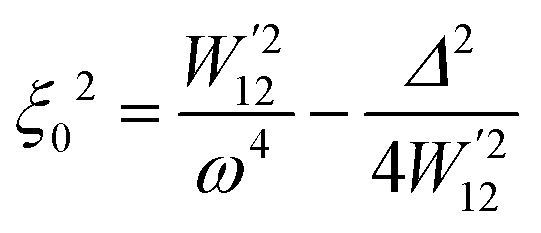 | (33) |
 .
.
Obviously when this condition is fulfilled, the low-temperature stable stage is ferroelectric, while the high-temperature one is paraelectric. The ferroelectric insecurity is incited at temperature TC, which, by putting in eqn (31), can be computed in the form of eqn (34), as follows:
 | (34) |
 approaches unity from beneath. Considering our presumptions concerning the type of ionic free vitality, this shakiness results exclusively from a vibronic coupling to the electronic movement. The more grounded the electron–phonon association parameter, the gentler the cross section (i.e. the smaller ω2), and the smaller the vitality band hole A, the less demanding the stage change can emerge.
Physically, the change emerges as the aftereffect of a reduction in the valence-band vitality by the electron–phonon association. In the event that the subsequent reduction in electronic vitality is bigger than the potential vitality of the grid modes portraying the dynamic vibrations, an unconstrained mutilation results. The presence of warm excitations between groups is not basic to this instrument, and for wide band holes, the ferroelectric unsteadiness in this model originates from the electronic potential term E(Ri, Rj, …) instead of the physically ionic potential U(Ri, Rj, …). Specifically, the commitment E(Ri, Rj, …) can be communicated expressly as far as the electron band and vibronic collaboration parameters, and subsequently the development coefficients of the subsequent aggregate compelling ionic potential V(Ri, Rj, …), prompting the potentials V and v to be isolated into their physically electronic and ionic parts. On account of the middle of the road or little band-hole circumstances, where electronic excitations are imperative, E(Ri, Rj…) progresses towards a temperature subordinate and an enhancement in the fundamental model along the lines set out above ends up basic for a quantitative hypothetical investigation. Although the main cause for ferroelectric instability is not yet fully discovered, the expected cause is due to the subtle steadiness between the short-range repulsions preferring the non-polar paraelectric phase and long-range Coulomb forces preferring the polar ferroelectric phase. Thus, for the ferroelectric phase to occur, the phase transition has to be from the non-polar paraelectric state to the polar phase. Not only the coexistence of properties and the main cause for ferroelectric instability but also the effect of lone pairs present in Pb metal on ferroelectricity, polarity and conductivity of halide perovskite materials still have to be discovered.
7.2 The influence of nanoscale defects
Ferroelectric materials are portrayed by an unconstrained polarization, which can be reoriented with a connected electric field. The switching between polarized domains is intervened by nanoscale defects. Thus, understanding the role of defects in ferroelectric switching is basic for practical applications, for example, non-volatile memories. This is particularly the situation for ferroelectric nanostructures and thin films in which the whole switching volume is proximate to an imperfect surface. Besides, these imperfections inside ferroelectric materials are generally grouped into two non-fundamentally unrelated classes depending on their impact on the free-vitality outline, i.e., random-field defect and random-bond defect. The first break the degeneracy of the polarization states to support at least one introduction and the second one changes the barrier height for advances between worse states. Interestingly, the most noticeable and voluminous defects in planar thin film heterostructures are the two interfaces, which break the precious crystal symmetry, as well as are joined by physical and synthetic recreations, bound charges, space charges and strain. These interfaces and deformities existing in ferroelectric films decide the qualities of ferroelectric exchanging, despite the fact that they have not yet been contemplated in halide perovskites. The impacts of the arbitrary field and irregular bond absconds are showed by changes in the nucleation inclinations of the nearby exchanges under the surface test. In addition, the vital impacts of inhomogeneities, for example, impurities and radiation damage, on the dielectric properties and switching conduct of ferroelectrics are of significant interest given that halide perovskites are delicate to radiation and light-actuated recreations, heterogeneity and order–disorder.155,334 Generally, defects in any crystalline lattice cause twisting of the encompassing volume and change in the neighborhood fields. The sizes of these impacts are harder to assess than the impacts of domain walls given that there are no 'mechanical-similarity' conditions and the degree of the precious crystal distortion relies on the idea of the defect, its site in the crystal, and the host-imperfection association. In an acentric site, an imperfection has a dipole minute related with it, as shown in eqn (35). | (35) |
 reflects the polar idea of the host, and thus
  is equivalent for every comparative imperfection inside a solitary area. In the event that the deformity focus N is adequately weakened that the connection between them can be dismissed, the naturally visible polarization change is shown by eqn (36), as follows:
 | (36) |
For example, when the polarization of a gem is switched by a connected field, the polarization ΔP because of the imperfections could possibly turn around. If it reverses, then the coercive field will rely on both the field required to switch the imperfections and the sign and magnitude of ΔP. Overall, the nearness of imperfections tends to expand the coercive field. In the event that ΔP does not turn around in an outer field, the deformities can markedly affect the exchanging properties relying on the dispersion of ΔP throughout the gem volume. In the unexpected case that every dipole has a similar sense, the hysteresis circles will seem one-sided, as shown in Fig. 23a. In case that the dipole introductions are requested over substantial locales, but the extraordinary districts are antiparallel, similar to a ferroelectric domain, at that point the hysteresis circles will appear as show in Fig. 23b. If the dipoles are totally irregular, as may occur in the event that they were brought into the crystal in a nonpolar phase, at that point the circle would seem typical with an expanded coercive field.
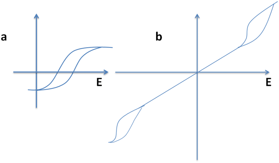 | ||
| Fig. 23 Biased hysteresis loops that may arise owing to the presence of defects in a ferroelectric crystal. (a) One-sided hysteresis circles, (b) antiparallel ferroelectric domain of hysteresis circles. | ||
7.3 Surface and bulk effects
To date, numerous trials have demonstrated that the ferroelectric nature on the surfaces of precious crystals is not quite the same as that in the bulk. Some of these observations have been made on as-developed precious crystals, where the substance idea of the surfaces may not be described in detail, for example the stoichiometry may be not the same as the bulk, or chemical adsorption may have happened.7.4 Material degradation effects
Generally, is well-known that halide perovskites are sensitive to moisture, temperature, light and ambient atmosphere.152 All these environmental factors cause degradation or at least deformation and property modifications of these materials, resulting in incorrect information. Thus, this subsection aims to urge the scientific community to carefully conduct their research considering all these factors. Recently, a perovskite solar cell showed an excellent stability of 2143 h of operation.515 This is promising operational stability for solar cells. However, the key problem is material instability while working on other applications beyond photovoltaics.8. Concluding remarks
Halide perovskites have emerged as promising materials for a wide range of applications such as in solar cells and other potential optoelectronic devices beyond photovoltaics due to their unique optoelectronic properties. Their better light absorption, charge carrier transport, higher to lower band gap range, potential opportunity for a variety of light absorbing families, potential opportunity for modification of the semiconductor formulation, variety of dimensions, structures, etc. have revolutionized a wide range of applications in science and technology. As a result of their uniqueness, single-junction perovskite solar cells demonstrated an appreciable development in PCE, beyond 27%, while perovskite/silicon tandem solar cell achieved an efficiency of above 34%. However, despite the appreciable development, the fundamental understanding of the device photophysics is not yet realized. Moreover, understanding the major applications beyond photovoltaics, the microscopic origin and mechanisms of their multifunctional properties, and increasing energy harvesting, nano-sensing and photoflexoelectric performances requires great consideration. Furthermore, new electronic applications such as piezoelectric nanogenerators, piezoelectric dampers, self-powered units and electromechanical devices are promising research topics in halide perovskite material nano-engineering research and cross-disciplinary energy materials research. Besides, the existence of a switchable spontaneous electric polarization creates piezoelectric and pyroelectric responses for use in many functions such as energy harvesting, photoflexoelectricity and nano-plasmonic sensing devices and thermoelectric applications. Therefore, developing general nano-engineering strategies for designing new energy harvesting, sensing and electromechanical responses is important and should get special attention.In addition, it is vital to understand the piezoelectric properties of halide perovskite materials. In particular, an enhancement in piezoelectric properties, piezoelectric applications and the suitability of their structure for reliable applications and efficient piezoelectric energy conversion are applicable research questions at this time. It is also still vital to know whether the symmetry of these materials is an important issue that should be considered during the study of their electronic properties and related applications. Furthermore, identifying the factors and issues influencing the clear understanding of these electrical parameters should be a future primary task in the field of halide perovskite study. In conclusion, we propose a new research direction for the development of halide perovskite research, focusing on the nano-engineering of polar order, strain, surface, domains and interfaces and thermodynamic concepts. To confirm whether halide perovskite materials possess all these electrical properties, developing advanced characterization spectroscopic techniques is highly relevant. Especially, nanometer-scale domain characterization tools such as AFM, PFM, PTIR, PiFM, nonlinear optical spectroscopy, SHG and first principles calculation impart the great interest for this purpose. In this review, the possible energy harvesting, sensing and electromechanical responses of halide perovskite applications beyond photovoltaic were reviewed and the big challenges for halide perovskite functionalization are highlighted to guide industries and research institutions.
To conclude with insightful ideas that will initiate researchers to conduct further investigations, this review will help researchers have an in-depth understanding on the origin and mechanisms of halide perovskite energy harvesting, photoflexoelectricity and nano-plasmonic sensing abilities as well as the nano-engineering innovative strategies required to design new multi-functional properties. Based on this perspective, there is a big question that needs a great answer. The first question is can halide perovskites achieve new breakthroughs and have the ability to revolutionize energy harvesting systems, photoflexoelectricity and nano-plasmonic sensing like in the photovoltaic field? The second great question is how can researchers rethink the halide perovskite field to bring a new paradigm shift in the way that new breakthroughs can be realized? The third question focuses on how to understand the bottleneck challenges in energy harvesting, nano-plasmonic sensing devices and photoflexoelectricity recalling the applications of halide perovskites? The fourth focuses on what pyroelectric configuration of energy harvesting can save energy loss or perform synergistic waste heat rejection to achieve photothermal heat to electricity conversion? This will address the issue of limited thermal fluctuation energy harvesting systems.
Furthermore, the global energy demand requires efficient device, effective procedures, and technological advances in manufacturing processes, device integration, and materials in piezoelectric energy for which halide perovskites are expected to meet and fit. Otherwise the sector for piezoelectric energy will fail to achieve its sustainable goals. Not only energy harvesting research but also nano-plasmonic sensing research will benefit from halide perovskites to meet its goal and solve the challenges limiting its expected application. The bottleneck challenge in nano-plasmonic sensing applications is detecting small molecules such as CO2, NO2, and O2 at a required concentration. The implementation of halide perovskites in nano-plasmonic sensing can solve this detection issue. Moreover, understanding the electron transport properties and underlying mechanisms during the detection process are the main strategies to nurture the application of halide perovskites for nano-plasmonic sensing. Moreover, integrating nano-plasmonic sensors with new technologies such as communication and digital technology with the application of halide perovskites is new area of research revolution. In this case, can halide perovskite-based nano-plasmonic sensors can improve the advanced integration suitable for modern technology? In addition, will combining halide perovskite-based plasmonic sensors with the Internet of Things (IoT), portable devices and smartphones bring new breakthroughs? This advanced integration into one platform demands in-depth technological innovations to create economical, simple and robust sensor kits. The issue here is that whether halide perovskites are useful.
Finally, photoflexoelectricity is a new potential application that enables both photovoltaic and electromechanical harvesting and transduction simultaneously. The origins for this possibility are the larger deformation, piezoelectric property, light and strain gradients of halide perovskites. The bottleneck challenge in photoflexoelectricity is the question if the enhanced light absorption and strain gradient can power the required flexoelectricity response. Now, can halide perovskites be potential candidates to solve the need for high light absorption and strain gradient to enhance the flexoelectricity response and power photoflexoelectricity? The answer for this issue depends on the semiconducting and flexoelectric synergistic properties of halide perovskites. These vital properties may also depend on the material structure, tilt sensing, piezoelectric, ferroelectric, and improved homogeneity of composites.516–518 All these suggestions should be investigated to successfully proceed in this research paradigm of energy harvesting, nano-plasmonic sensing and photoflexoelectricity. In line with these big challenges, the issues of stability, toxicity and defects are equally important to revolutionize these new perspectives. Finally, not only limited power supply, controlling resonant frequency, and intermittent nature of ambient kinetic energy input but also dielectric, piezoelectric and elastic losses are the bottleneck challenges in energy harvesting devices. Would it be possible for halide perovskites to break all these bottleneck challenges, and hence enable the performance of energy harvesters and empower the market of the self-powered sensors? This great concluding remark is forwarded to the perovskite scientific community, research enterprises and development industries to devote their efforts to solving these big challenges.
Author contributions
Dr Taame Abraha Berhe has designed and organized the conceptualization, data curation, formal analysis, writing – original draft of this review based on the current state of halide perovskites. Etsana Kiros Ashebir has collected new papers from reputable journals resources writing-review and editing, and ordered all references based on their importance in this review. Prof. Wei-Nien Su has confirmed the harmony, validation, software and ethical considerations of this review as well as making this review easy to understand for the general readership. Prof. Bing Joe Hwang has supervised this review for all its funding acquisition, suitability and coverage of all pertinent areas in the field of halide perovskites.Data availability
All data are included within the manuscript.Conflicts of interest
The authors declare no conflict of interest.Acknowledgements
This work was financially supported by the Ministry of Science and Technology (MoST) (106-2923-E 011-005, 105-3113-E-011-001, 105-ET-E-011-004-ET, 104-2923-M-011-002-MY3, 104-2911-1-011-505-MY2, 103-2221-E-011-156-MY3), the Top University Projects (100H45140), the Global Networking Talent 3.0 Plan (NTUST 104DI005) from the Ministry of Education of Taiwan, Taiwan's Deep Decarbonization Pathways toward a Sustainable Society Project (106-0210-02-11-03) from Academia Sinica as well as the facilities of support from Adigrat University, National Taiwan University of Science and Technology (NTUST) and National Synchrotron Radiation Research Centre (NSRRC) are also acknowledged.References
- J. Liu, Y. He, L. Ding, H. Zhang, Q. Li, L. Jia, J. Yu, T. W. Lau, M. Li, Y. Qin, X. Gu, F. Zhang, Q. Li, Y. Yang, S. Zhao, X. Wu, J. Liu, T. Liu, Y. Gao, Y. Wang, X. Dong, H. Chen, P. Li, T. Zhou, M. Yang, X. Ru, F. Peng, S. Yin, M. Qu, D. Zhao, Z. Zhao, M. Li, P. Guo, H. Yan, C. Xiao, P. Xiao, J. Yin, X. Zhang, Z. Li, B. He and X. Xu, Nature, 2024, 635, 596–603 CrossRef CAS PubMed.
- Y. Chen, Z. Yang, M. Wang, Y. Zhang, Y. Bao, L. Shi, G. Cao, L. Qin and X. Li, Nano Energy, 2024, 132, 110366 CrossRef.
- S. Rühle, Sol. Energy, 2016, 130, 139–147 CrossRef.
- A. Richter, M. Hermle and S. W. Glunz, IEEE J. Photovolt., 2013, 3, 1184–1191 Search PubMed.
- L. Jonathan, L. J. Diguna, O. Samy, M. Muqoyyanah, S. Abu Bakar, M. D. Birowosuto and A. El Moutaouakil, Polymers, 2022, 14, 1059 CrossRef CAS PubMed.
- S. Gong, G. Qu, Y. Qiao, Y. Wen, Y. Huang, S. Cai, L. Zhang, K. Jiang, S. Liu, M. Lin, M. C. Beard, Z.-X. Xu and X. Chen, Energy Environ. Sci., 2024, 17, 5080–5090 RSC.
- A. Miyata, A. Mitioglu, P. Plochocka, O. Portugall, J. T.-W. Wang, S. D. Stranks, H. J. Snaith and R. J. Nicholas, Nat. Phys., 2015, 11, 582 Search PubMed.
- C. Wehrenfennig, G. E. Eperon, M. B. Johnston, H. J. Snaith and L. M. Herz, Adv. Mater., 2014, 26, 1584–1589 CrossRef CAS PubMed.
- J. M. Frost, K. T. Butler, F. Brivio, C. H. Hendon, M. van Schilfgaarde and A. Walsh, Nano Lett., 2014, 14, 2584–2590 CrossRef CAS PubMed.
- S. Liu, F. Zheng, I. Grinberg and A. M. Rappe, J. Phys. Chem. Lett., 2016, 7, 1460–1465 CrossRef CAS PubMed.
- M. Coll, A. Gomez, E. Mas-Marza, O. Almora, G. Garcia-Belmonte, M. Campoy-Quiles and J. Bisquert, J. Phys. Chem. Lett., 2015, 6, 1408–1413 CrossRef CAS PubMed.
- D. Seol, G. S. Han, C. Bae, H. Shin, H. S. Jung and Y. Kim, J. Mater. Chem. A, 2015, 3, 20352–20358 RSC.
- Q. F. Dong, J. F. Song, Y. J. Fang, Y. C. Shao, S. Ducharme and J. S. Huang, Adv. Mater., 2016, 28, 2816 CrossRef CAS PubMed.
- R. Ding, H. Liu, X. Zhang, J. Xiao, R. Kishor, H. Sun, B. Zhu, G. Chen, F. Gao, X. Feng, J. Chen, X. Chen, X. Sun and Y. Zheng, Adv. Funct. Mater., 2016, 26, 7708–7716 CrossRef CAS.
- Y.-J. Kim, T.-V. Dang, H.-J. Choi, B.-J. Park, J.-H. Eom, H.-A. Song, D. Seol, Y. Kim, S.-H. Shin, J. Nah and S.-G. Yoon, J. Mater. Chem. A, 2016, 4, 756–763 RSC.
- E. Strelcov, Q. Dong, T. Li, J. Chae, Y. Shao, Y. Deng, A. Gruveman, J. Huang and A. Centrone, Sci. Adv., 2016, 3, e1602165 CrossRef PubMed.
- B. Huang, Z. Liu, C. Wu, Y. Zhang, J. Zhao, X. Wang and J. Li, Natl. Sci. Rev., 2021, 8, nwab094 CrossRef CAS PubMed.
- Y. Zhou, L. You, S. W. Wang, Z. L. Ku, H. J. Fan, D. Schmidt, A. Rusydi, L. Chang, L. Wang, P. Ren, L. F. Chen, G. L. Yuan, L. Chen and J. L. Wang, Nat. Commun., 2016, 7, 11193 CrossRef CAS PubMed.
- J. M. Frost, K. T. Butler, T. Keith and A. Walsh, APL Mater., 2014, 2, 081506 CrossRef.
- S. Liu, F. Zheng, N. Z. Koocher, H. Takenaka, F. Wang and A. M. Rappe, J. Phys. Chem. Lett., 2015, 6, 693 CrossRef CAS PubMed.
- T. M. Brenner, D. A. Egger, L. Kronik, G. Hodes and D. Cahen, Nat. Rev. Mater., 2016, 1, 15007 CrossRef CAS.
- D. Li, H. Wu, H. C. Cheng, G. Wang, Y. Huang and X. Duan, ACS Nano, 2016, 10, 6933–6941 CrossRef CAS PubMed.
- A. Varughese, R. Kaur and P. Singh, IOP Conf. Ser.:Mater. Sci. Eng., 2020, 961, 012011 CAS.
- H. Kim, K.-G. Lim and T.-W. Lee, Energy Environ. Sci., 2016, 9, 12–30 RSC.
- J. H. Heo, D. H. Song, H. J. Han, S. Y. Kim, J. H. Kim, D. Kim, H. W. Shin, T. K. Ahn, C. Wolf, T.-W. Lee and S. H. Im, Adv. Mater., 2015, 27, 3424–3430 CrossRef CAS PubMed.
- R. Inoue, S. Ishikawa, R. Imura, Y. Kitanaka, T. Oguchi, Y. Noguchi and M. Miyayama, Sci. Rep., 2015, 5, 14741 CrossRef CAS PubMed.
- H. Han, D. Kim, S. Chae, J. Park, S. Y. Nam, M. Choi, K. Yong, H. J. Kim, J. Son and H. M. Jang, Nanoscale, 2018, 10, 13261–13269 RSC.
- L. You, F. Zheng, L. Fang, Y. Zhou, L. Z. Tan, Z. Zhang, G. Ma, D. Schmidt5, A. Rusydi, L. Wang, L. Chang, A. M. Rappe and J. Wang, Sci. Adv., 2018, 4, eaat3438 CrossRef PubMed.
- B. Chen, J. Shi, X. Zheng, Y. Zhou, K. Zhu and S. Priya, J. Mater. Chem. A, 2015, 3, 7699–7705 RSC.
- J. Zhang, X. Su, M. Shen, Z. Dai, L. Zhang, X. He, W. Cheng, M. Cao and G. Zou, Sci. Rep., 2013, 3, 2109 CrossRef PubMed.
- P. C. Harikesh, B. Wu, B. Ghosh, R. A. John, S. Lie, K. Thirumal, L. H. Wong, T. C. Sum, S. Mhaisalkar and N. Mathews, Adv. Mater., 2018, 30, 1802080 CrossRef PubMed.
- V. Fridkin, Crystallogr. Rep., 2001, 46, 654–658 CrossRef.
- L. Pintilie, I. Vrejoiu, G. Le Rhun and M. Alexe, J. Appl. Phys., 2007, 101, 064109 CrossRef.
- J. Oh, H. C. Yuan and H. M. Branz, Nat. Nanotechnol., 2012, 7, 743–748 CrossRef CAS PubMed.
- B. O’Regan and M. Gratzel, Nature, 1991, 353, 737–740 CrossRef.
- S. R. Wenham, M. A. Green, M. E. Watt and R. Corkish, Applied Photovoltaics, Earthscan Ltd, London, 2006 Search PubMed.
- D. G. McGehee, Nat. Photonics, 2009, 3, 250–252 CrossRef.
- H. S. Nalwa, Handbook of Organic Electronics and Photonics, American Scientific Publishers, USA, 2008 Search PubMed.
- B. Chen, J. Shi, X. Zheng, Y. Zhou, K. Zhu and S. Priya, J. Mater. Chem. A, 2015, 3, 7699–7705 RSC.
- S. M. Young, F. Zheng and A. M. Rappe, Phys. Rev. Lett., 2012, 109, 236601 CrossRef PubMed.
- A. M. Glass, V. D. Linde and T. J. Negran, Appl. Phys. Lett., 1974, 25, 233 CrossRef CAS.
- S. Y. Yang, J. Seidel, S. J. Byrnes, P. Shafer, C.-H. Yang, M. D. Rossell, P. Yu, Y.-H. Chu, J. F. Scott, J. W. AgerIII, L. W. Martin and R. Ramesh, Nat. Nanotechnol., 2010, 5, 143–147 CrossRef CAS PubMed.
- A. Bhatnagar, A. R. Chaudhuri, Y. H. Kim, D. Hesse and M. Alexe, Nat. Commun., 2013, 4, 2835 Search PubMed.
- H. Y. Ye, W. Q. Liao, C. L. Hu, Y. Zhang, Y. M. You, J. G. Mao, P. F. Li and R. G. Xiong, Adv. Mater., 2016, 28, 2579–2586 Search PubMed.
- H.-Y. Zhang, Z. Wei, P.-F. Li, Y.-Y. Tang, W.-Q. Liao, H.-Y. Ye, H. Cai and R.-G. Xiong, Angew. Chem., Int. Ed., 2018, 57, 526–530 CrossRef CAS PubMed.
- M. Ahmadi, T. Wu and B. Hu, et al. , Adv. Mater., 2017, 29, 1605242 CrossRef PubMed.
- E. Strelcov, Q. Dong, T. Li, J. Chae, Y. Shao, Y. Deng, A. Gruverman, J. Huang and A. Centrone, Sci. Adv., 2017, 3, e1602165 CrossRef PubMed.
- G. Gou and J. M. Rondinelli, Adv. Mater. Interfaces, 2014, 1, 1400042 CrossRef.
- Y. Li, M. Behtash, J. Wong and K. Yang, J. Phys. Chem. C, 2018, 122, 177–184 CrossRef CAS.
- Y. Chen, Y. Lei, Y. Li, Y. Yu, J. Cai, M.-H. Chiu, R. Rao, Y. Gu, C. Wang, W. Choi, H. Hu, C. Wang, Y. Li, J. Song, J. Zhang, B. Qi, M. Lin, Z. Zhang, A. E. Islam, B. Maruyama, S. Dayeh, L.-J. Li, K. Yang, Y.-H. Lo and S. Xu, Nature, 2020, 577, 209–215 CrossRef CAS PubMed.
- R. A. Surmenev and M. A. Surmeneva, Mater. Today, 2023, 67, 256–298 CrossRef.
- B. Yang, D. Bogachuk, J. Suo, L. Wagner, H. Kim, J. Lim, A. Hinsch, G. Boschloo, M. Nazeeruddin and A. Hagfeldt, Chem. Soc. Rev., 2022, 51, 7509–7530 RSC.
- S. Nazir, M. Behtash and K. Yang, Appl. Phys. Lett., 2014, 105, 141602 CrossRef.
- K. Yang, W. Setyawan, S. Wang, M. B. Nardelli and S. Curtarolo, Nat. Mater., 2012, 11, 614–619 CrossRef CAS PubMed.
- M.-J. Choi, J. W. Lee and H. Jang, Adv. Mater., 2023, 36, e2308827 CrossRef PubMed.
- J. Zhao, Y. Deng, H. Wei, X. Zheng, Z. Yu, Y. Shao, J. E. Shield and J. Huang, Sci. Adv., 2017, 3, eaao5616 CrossRef PubMed.
- V. Keppens, Nat. Mater., 2013, 12, 952–953 CrossRef CAS PubMed.
- D. B. Kim, J. Y. Kim, J. Han and Y. S. Cho, Nano Energy, 2024, 125, 109551 CrossRef CAS.
- N. Muralidharan, R. Carter, L. Oakes, A. P. Cohn and C. L. Pint, Sci. Rep., 2016, 6, 27542 CrossRef CAS PubMed.
- S. S. Won, H. Seo, M. Kawahara, S. Glinsek, J. Lee, Y. Kim, C. K. Jeong, A. I. Kingon and S.-H. Kim, Nano Energy, 2019, 55, 182–192 CrossRef CAS.
- D. Liu, D. Luo, A. N. Iqbal, K. W. P. Orr, T. A. S. Doherty, Z.-H. Lu, S. D. Stranks and W. Zhang, Nat. Mater., 2021, 20, 1337–1346 CrossRef CAS PubMed.
- W. Meng, K. Zhang, A. Osvet, J. Zhang, W. Gruber, K. Forberich, B. Meyer, W. Heiss, T. Unruh, N. Li and C. J. Brabec, Joule, 2022, 6, 458–475 CrossRef CAS.
- J. Liu, M. P. Garman, J. Dong, B. van der Zee, L. Qiu, G. Portale, J. C. Hummelen and L. J. A. Koster, ACS Appl. Energy Mater., 2019, 2, 6664–6671 CrossRef CAS.
- X. Yu, Y. Hou, M. Zheng, J. Yan, W. Jia and M. Zhu, J. Am. Ceram. Soc., 2019, 102, 275–284 CrossRef CAS.
- Y. Zhong, Y.-E. Huang, T. Deng, Y.-T. Lin, X.-Y. Huang, Z.-H. Deng and K.-Z. Du, Inorg. Chem., 2021, 60, 17357–17363 CrossRef CAS PubMed.
- E. Arkan, A. Karabiber, M. A. Topçu, Z. Kinas, A. Sarilmaz, S. S. Ozel and F. Ozel, Surf. Interfaces, 2023, 37, 102683 CrossRef CAS.
- M. Martín-González, O. Caballero-Calero and P. Díaz-Chao, Renewable Sustainable Energy Rev., 2013, 24, 288–305 CrossRef.
- X. Yu, L. Zhu, X. Li, J. Zhao, T. Wu, W. Yu and W. Li, Materials, 2023, 16, 1778 CrossRef CAS PubMed.
- W. Yao, L. Shen, P. Liu, C. Liu, J. Xu, Q. Jiang, G. Liu, G. Nie and F. Jiang, Mater. Chem. Front., 2020, 4, 597–604 RSC.
- N. K. Sinha, P. Roy, D. S. Ghosh and A. Khare, Mater. Today: Proc., 2023, 83, 6–13 CAS.
- S. Jiang, M. Liu, D. Zhao, Y. Guo, J. Fu, Y. Lei, Y. Zhang and Z. Zheng, Phys. Chem. Chem. Phys., 2024, 26, 4794–4811 RSC.
- C. He, J. Qiu, Z. Mu and X. Liu, CCS Chem., 2023, 5, 1961–1972 CrossRef CAS.
- Y. Lin, Y. Zhong, Y. Lin, J. Lin, L. Pang, Z. Zhang, Y. Zhao, X.-Y. Huang and K.-Z. Du, Front. Optoelectron., 2024, 17, 6 CrossRef PubMed.
- T. J. Jacobsson, J.-P. Correa-Baena, M. Pazoki, M. Saliba, K. Schenk, M. Gratzel and A. Hagfeldt, Energy Environ. Sci., 2016, 9, 1706–1724 RSC.
- W.-L. Yan, G.-H. Lu and F. Liu, J. Phys. Chem. C, 2016, 120, 17972–17977 CrossRef CAS.
- L. Atourki, E. Vegar, B. Mar, M. Mollar, H. A. Ahsaine, K. Bouabid and A. Ihlal, Appl. Surf. Sci., 2016, 371, 112–117 CrossRef CAS.
- A. Stroppa, D. D. Sante and P. Barone, et al. , Nat. Commun., 2014, 5, 5900 CrossRef CAS PubMed.
- A. Stroppa, P. Jain and P. Barone, et al. , Angew. Chem., 2011, 123, 5969–5972 CrossRef.
- A. Stroppa, P. Barone and P. Jain, et al. , Adv. Mater., 2013, 25, 2284–2290 CrossRef CAS PubMed.
- D. D. Sante, A. Stroppa and P. Jain, et al. , J. Am. Chem. Soc., 2013, 135, 18126–18130 CrossRef PubMed.
- S. Bhatti, C. Ma, X. Liu and S. N. Piramanayagam, IEEE Trans. Magn., 2019, 55, 1–7 Search PubMed.
- S. Pruvost, A. Hajjaji, L. Lebrun, D. Guyomar and Y. Boughaleb, J. Phys. Chem. C, 2010, 114, 20629–20635 CrossRef CAS.
- A. R. Balakrishna and J. E. Huber, Smart Mater. Struct., 2016, 25, 104001 CrossRef.
- W.-J. Xu, S. Kopyl, A. Kholkin and J. Rocha, Coord. Chem. Rev., 2019, 387, 398–414 CrossRef CAS.
- S.-E. Park and T. R. Shrout, J. Appl. Phys., 1997, 82, 1804–1811 CrossRef CAS.
- J. Mannhart and D. G. Schlom, Science, 2010, 327, 1607–1611 CrossRef CAS PubMed.
- H. Y. Hwang, Y. Iwasa, M. Kawasaki, B. Keimer, N. Nagaosa and Y. Tokura, Nat. Mater., 2012, 11, 103–113 CrossRef CAS PubMed.
- J. A. Mundy, C. M. Brooks, M. E. Holtz, J. A. Moyer, H. Das, A. F. Rébola, J. T. Heron, J. D. Clarkson, S. M. Disseler, Z. Liu, A. Farhan, R. Held, R. Hovden, E. Padgett, Q. Mao, H. Paik, R. Misra, L. F. Kourkoutis, E. Arenholz, A. Scholl, J. A. Borchers, W. D. Ratcliff, R. Ramesh, C. J. Fennie, P. Schiffer, D. A. Muller and D. G. Schlom, Nature, 2016, 537, 523–527 CrossRef CAS PubMed.
- S. Dong, J.-M. Liu, S.-W. Cheong and Z. Ren, Adv. Phys., 2015, 64, 519–626 CrossRef CAS.
- M. Stengel, D. Vanderbilt and N. A. Spaldin, Nat. Mater., 2009, 8, 392–397 CrossRef CAS PubMed.
- E. Bousquet, M. Dawber, N. Stucki, C. Lichtensteiger, P. Hermet, S. Gariglio, J. M. Triscone and P. Ghosez, Nature, 2008, 452, 732–736 CrossRef CAS PubMed.
- Y. L. Tang, Y. L. Zhu, X. L. Ma, A. Y. Borisevich, A. N. Morozovska, E. A. Eliseev, W. Y. Wang, Y. J. Wang, Y. B. Xu, Z. D. Zhang and S. J. Pennycook, Science, 2015, 348, 547–551 CrossRef CAS PubMed.
- Y. Kutes, L. Ye, Y. Zhou, S. Pang, B. D. Huey and N. P. Padture, J. Phys. Chem. Lett., 2014, 3335–3339 CrossRef CAS PubMed.
- D. Chen, Z. Chen, Q. He, J. D. Clarkson, C. R. Serrao, A. K. Yadav, M. E. Nowakowski, Z. Fan, L. You, X. Gao, D. Zeng, L. Chen, A. Y. Borisevich, S. Salahuddin, J.-M. Liu and J. Bokor, Nano Lett., 2017, 17, 486–493 CrossRef CAS PubMed.
- G. Arlt, J. Mater. Sci., 1990, 25, 2655–2666 CrossRef CAS.
- R. E. Newnham, Structure–Property Relations, Springer-Verlag, Berlin, 1975 Search PubMed.
- W. R. Cook, J. Am. Ceram. Soc., 1956, 39, 17–19 CrossRef CAS.
- R. Pandey, G. Sb, S. Grover, S. K. Singh, A. Kadam, S. Ogale, U. V. Waghmare, V. R. Rao and D. Kabra, ACS Energy Lett., 2019, 4, 1004–1011 CrossRef CAS.
- S. Ippili, J. H. Kim, V. Jella, S. Behera, V.-H. Vuong, J.-S. Jung, Y. Cho, J. Ahn, I.-D. Kim, Y. H. Chang, H.-S. Kim and S.-G. Yoon, Nano Energy, 2023, 107, 108148 CrossRef CAS.
- M. M. Rana, A. A. Khan, W. Zhu, M. F. A. Fattah, S. Kokilathasan, S. Rassel, R. Bernard, S. Ababou-Girard, P. Turban, S. Xu, C. Wang and D. Ban, Nano Energy, 2022, 101, 107631 CrossRef CAS.
- T. Zhang, K. Xu, J. Li, L. He, D.-W. Fu, Q. Ye and R.-G. Xiong, Natl. Sci. Rev., 2023, 10, nwac240 CrossRef CAS PubMed.
- L. Hy and Z. Hy, J. Am. Chem. Soc., 2020, 142, 15205–15218 CrossRef PubMed.
- V. Jella, S. Ippili and S.-G. Yoon, ACS Appl. Electron. Mater., 2020, 2, 2579–2590 CrossRef CAS.
- J. Breternitz, F. Lehmann and S. A. Barnett, et al. , Angew. Chem., Int. Ed., 2020, 59, 424–428 CrossRef CAS PubMed.
- P. Gao, H.-J. Liu, Y.-L. Huang, Y.-H. Chu, R. Ishikawa, B. Feng, Y. Jiang, N. Shibata, E.-G. Wang and Y. Ikuhara, Nat. Commun., 2016, 7, 11318 CrossRef CAS PubMed.
- L. C. An, K. Li and Z. G. Li, et al. , Small, 2021, 17, e2006021 CrossRef PubMed.
- W. Q. Liao, Y. Y. Tang and P. F. Li, et al. , J. Am. Chem. Soc., 2018, 140, 3975–3980 CrossRef CAS PubMed.
- T. Bokdam, M. Sander, A. Stroppa, S. Picozzi, D. D. Sarma, C. Franchini and G. Kresse, Sci. Rep., 2016, 6, 28618 CrossRef PubMed.
- J.-B. Li, Z.-K. Jiang, R. Wang, J.-Z. Zhao and R. Wang, npj Comput. Mater., 2023, 9, 62 CrossRef CAS.
- N. J. Jeon, J. H. Noh, W. S. Yang, Y. C. Kim, S. Ryu, J. Seo and S. I. Seok, Nature, 2015, 517, 476–480 CrossRef CAS PubMed.
- F. Igbari, R. Wang, Z.-K. Wang, X.-J. Ma, Q. Wang, K.-L. Wang, Y. Zhang, L.-S. Liao and Y. Yang, Nano Lett., 2019, 19, 2066–2073 CrossRef CAS PubMed.
- J. Zhou, Z. Xia, M. S. Molokeev, X. Zhang, D. Peng and Q. Liu, J. Mater. Chem. A, 2017, 5, 15031–15037 RSC.
- K. A. Bush, K. Frohna, R. Prasanna, R. E. Beal, T. Leijtens, S. A. Swifter and M. D. McGehee, ACS Energy Lett., 2018, 3, 428–435 CrossRef CAS.
- M. R. Linaburg, E. T. McClure, J. D. Majher and P. M. Woodward, Chem. Mater., 2017, 29, 3507–3514 CrossRef CAS.
- M. B. Gray, E. T. McClure and P. M. Woodward, J. Mater. Chem. C, 2019, 7, 9686–9689 RSC.
- Y. Liu, et al. , Nat. Mater., 2018, 17, 1013–1019 CrossRef CAS PubMed.
- D. Lee, S. H. Baek, T. H. Kim, J.-G. Yoon, C. M. Folkman, C. B. Eom and T. W. Noh, Phys. Rev., 2011, B84, 125305 CrossRef.
- C. Chen, L. Gao and W. Gao, Nat. Commun., 2019, 10, 1927 CrossRef PubMed.
- P. J. Huang, K. Taniguchi and H. Miyasaka, J. Am. Chem. Soc., 2019, 141, 14520–14523 CrossRef CAS PubMed.
- L. Even, J. Pedesseau, J.-M. Jancu and C. Katan, J. Phys. Chem. Lett., 2013, 4, 2999–3005 CrossRef.
- F. E. Mellouhi, E. T. Bentria, A. Marzouk, S. N. Rashkeev, S. Kais and F. H. Alharbi, npj Comput. Mater., 2016, 2, 16035 CrossRef.
- G. King and P. M. Woodward, J. Mater. Chem., 2010, 20, 5785–5796 RSC.
- G. Pilaniaa and B. P. Uberuaga, J. Appl. Phys., 2015, 117, 114103 CrossRef.
- E. Amat, A. Mosconi, E. Ronca, C. Quarti, P. Umari, M. K. Nazeeruddin, M. Grätzel and F. D. Angelis, Nano Lett., 2014, 14, 3608–3616 CrossRef PubMed.
- J. Kim, H. Kim, M. Chandran, S.-C. Lee, S. H. Im and K.-H. Hong, APL Mater., 2018, 6, 084903 CrossRef.
- J. V. Passarelli, D. J. Fairfield and N. A. Sather, J. Am. Chem. Soc., 2018, 140, 7313–7323 CrossRef CAS PubMed.
- C. Katan, N. Mercier and J. Even, Chem. Rev., 2019, 119, 3140–3192 CrossRef CAS PubMed.
- X. G. Chen, X. J. Song and Z. X. Zhang, et al. , J. Am. Chem. Soc., 2020, 142, 10212–10218 CrossRef CAS PubMed.
- M. G. Mączka, A. Ptak, M. Paraguassu, W. da Silva, T. A. Sieradzki and A. A. Pikul, Chem. Mater., 2017, 29, 2264–2275 CrossRef.
- M. Mączka, M. Ptak, A. Gągor, D. Stefańska and A. Sieradzki, Chem. Mater., 2019, 31, 8563–8575 CrossRef.
- M. P. Mączka, M. Gągor, A. Stefańska and D. A. Sieradzki, Chem. Mater., 2019, 31, 8563–8575 CrossRef.
- W. Q. Liao, D. W. Zhao, Y. Y. Tang, Y. Zhang, P. F. Li, P. P. Shi, X. G. Chen, Y. M. You and R. G. Xiong, Science, 2019, 363, 1206–1210 CrossRef CAS PubMed.
- Y. Rakita, O. B. Elli, E. Meirzadeh, H. Kaslasi, Y. Peleg, G. Hodes, I. Lubomirsky, D. Oron, D. Ehre and D. Cahen, Proc. Natl. Acad. Sci. U. S. A., 2017, 114, E5504–E5512 CrossRef CAS PubMed.
- D. A. Berlincourt, D. R. Curran and H. Jaffe, Physical Acoustics: Principles and Methods, 1964, vol. 1(Part A), pp. 202–204 Search PubMed.
- Z.-R. Gao, X.-F. Sun, Y.-Y. Wu, Y.-Z. Wu, H.-L. Cai and X. S. Wu, J. Phys. Chem. Lett., 2019, 10, 2522–2527 CrossRef CAS PubMed.
- B. Liu, M. Long, M.-Q. Cai, X. Hao and J. Yang, J. Phys. Chem. C, 2018, 122, 17820–17824 CrossRef CAS.
- F. Ke, J. Yan, S. Niu, J. Wen, K. Yin, H. Yang, N. R. Wolf, Y.-K. Tzeng, H. I. Karunadasa, Y. S. Lee, W. L. Mao and Y. Lin, Nat. Commun., 2022, 13, 7067 CrossRef CAS PubMed.
- S. Colella, E. Mosconi, P. Fedeli, A. Listorti, F. Gazza, F. Orlandi, P. Ferro, T. Besagni, A. Rizzo, G. Calestani, G. Gigli, F. De Angelis and R. Mosca, Chem. Mater., 2013, 25, 4613–4618 CrossRef CAS.
- W. Guo, X. Liu and S. Han, et al. , Angew. Chem., Int. Ed., 2020, 59, 13879–13884 CrossRef CAS PubMed.
- W. Y. Zhang, Y. Y. Tang and P. F. Li, et al. , J. Am. Chem. Soc., 2017, 139, 10897–10902 CrossRef CAS PubMed.
- H. Y. Zhang, X. G. Chen and Z. X. Zhang, et al. , Adv. Mater., 2020, 32, 2005213 CrossRef CAS.
- Q. Pan, Z. B. Liu and Y. Y. Tang, et al. , J. Am. Chem. Soc., 2017, 139, 3954–3957 CrossRef CAS PubMed.
- M. G. Ehrenreich, Z. Zeng, S. Burger, M. R. Warren, M. W. Gaultois, J.-C. Tan and G. Kieslich, Chem. Commun., 2019, 55, 3911–3914 RSC.
- J. Xiao, J. Chang, B. Li, F. H. Isikgor, D. Wang, Z. Fan, Z. Lin, J. Ouyang, K. Zeng and J. Chen, J. Mater. Chem. A, 2018, 6, 9665–9676 RSC.
- A. Iefanova, N. Adhikari, A. Dubey, D. Khatiwada and Q. Qiao, AIP Adv., 2016, 6, 085312 CrossRef.
- H. Wei, Y. L. Yang, S. Y. Chen and H. J. Xiang, Nat. Commun., 2021, 12, 1–8 CrossRef.
- C. C. Stoumpos, C. D. Malliakas and M. G. Kanatzidis, Inorg. Chem., 2013, 52, 9019–9038 CrossRef CAS.
- M. Caputo, N. Cefarin, A. Radivo, N. Demitri, L. Gigli, J. R. Plaisier, M. Panighel, G. Di Santo, S. Moretti, A. Giglia, M. Polentarutti, F. De Angelis, E. Mosconi, P. Umari, M. Tormen and A. Goldoni, Sci. Rep., 2019, 9, 15159 CrossRef.
- A. Sagdeo, S. Dutt, O. V. Rambadey and P. R. Sagdeo, Absence of Ferroelectricity in Organic–Inorganic Hybrid Perovskite Methylammonium Lead Chloride Single Crystal, Mapbcl3, Available at SSRN: https://ssrn.com/abstract=4198120 or DOI:10.2139/ssrn.4198120, 2022.
- S. Dutt, O. V. Rambadey, P. R. Sagdeo and A. Sagdeo, Mater. Chem. Phys., 2023, 295, 127169 CrossRef CAS.
- M. Bari, A. A. Bokov and Z.-G. Ye, J. Mater. Chem. C, 2020, 8, 9625–9631 RSC.
- T. A. Berhe, W.-N. Su, C.-H. Chen, C.-J. Pan, J.-H. Cheng, H.-M. Chen, M.-C. Tsai, L.-Y. Chen, A. A. Dubale and B.-J. Hwang, Energy Environ. Sci., 2016, 9, 323–356 RSC.
- J. Fan, B. Jia and M. Gu, Photonics Res., 2014, 2, 111–120 Search PubMed.
- C. He and X. Liu, Light: Sci. Appl., 2023, 12, 15 CrossRef CAS PubMed.
- T. Leijtens, G. E. Eperon, S. Pathak, A. Abate, M. M. Lee and H. J. Snaith, Nat. Commun., 2013, 4, 2885 CrossRef PubMed.
- P. Gao, A. R. Bin-Mohd Yusoff and M. K. Nazeeruddin, Nat. Commun., 2018, 9, 5028 CrossRef PubMed.
- P. Wannasut, P. Jaiban, P. Jaita, M. Promsawat, O. Khamman and A. Watcharapasorn, J. Australas. Ceram. Soc., 2023, 11, 88–97 CrossRef.
- T. Leijtens, E. Hoke, G. Grancini, D. Slotcavage, G. Eperon, J. Ball, M. De Bastiani, A. Bowring, N. Martino, K. Wojciechowski, M. McGehee, H. Snaith and A. Petrozza, Adv. Energy Mater., 2015, 5, 1500962 CrossRef.
- C. Zhang, D. Sun, X. Liu, C.-X. Sheng and Z. V. Vardeny, J. Phys. Chem. Lett., 2017, 8, 1429–1435 CrossRef CAS PubMed.
- G. A. Sewvandi, K. Kodera, H. Ma, S. Nakanishi and Q. Feng, Sci. Rep., 2016, 6, 30680 CrossRef CAS PubMed.
- M. E. Kiziroglou and E. M. Yeatman, in Functional Materials for Sustainable Energy Applications, ed. J. A. Kilner, S. J. Skinner, S. J. C. Irvine and P. P. Edwards, Woodhead Publishing, Imperial College London, UK, 2012, ch. 5, pp. 541–572 Search PubMed.
- H. Wang and A. Jasim, in Eco-Efficient Pavement Construction Materials, ed. F. Pacheco-Torgal, S. Amirkhanian, H. Wang and E. Schlangen, Woodhead Publishing in Civil and Structural Engineering, UK, 2020, ch. 5, pp. 367–382 Search PubMed.
- H. Röhm, T. Leonhard, A. D. Schulz, S. Wagner, M. J. Hoffmann and A. Colsmann, Adv. Mater., 2019, 31, 1806661 CrossRef PubMed.
- S. Hu, H. Gao, Y. Qi, Y. Tao, Y. Li, J. R. Reimers, M. Bokdam, C. Franchini, D. D. Sante, A. Stroppa and W. Ren, J. Phys. Chem. C, 2017, 121, 23045–23054 CrossRef CAS.
- J. Guyonnet, Domain walls in ferroelectric materials, Ferroelectric Domain Walls, Springer Theses Springer International Publishing, Basel, Switzerland, 2014 Search PubMed.
- Y. Z. Hu, L. You and B. Xu, et al. , Nat. Mater., 2021, 20, 612–617 CrossRef CAS PubMed.
- H. Röhm, T. Leonhard, M. J. Hoffmann and A. Colsmann, Energy Environ. Sci., 2017, 10, 950–955 RSC.
- A. Puhan, B. Bhushan, A. K. Nayak and D. Rout, in Fundamentals and Properties of Multifunctional Nanomaterials, ed. S. Thomas, N. Kalarikkal and A. R. Abraham, Elsevier, 2021, ch. 5, pp. 275–293 Search PubMed.
- R. F. Mueller, Order-disorder In: Mineralogy. Encyclopedia of Earth Science, Springer, Boston, 1983, pp. 344–348 Search PubMed.
- K. Fykouras, J. Lahnsteiner, N. Leupold, P. Tinnemans, R. Moos, F. Panzer, G. A. de Wijs, M. Bokdam, H. Grüninger and A. P. M. Kentgens, J. Mater. Chem. A, 2023, 11, 4587–4597 RSC.
- O. Yaffe, Y. Guo, T. Hull, C. Stoumpos, L. Tan, D. Egger, F. Zheng, G. Szpak, O. Semonin, A. Beecher, T. Heinz, L. Kronik, A. Rappe, M. Kanatzidis, J. Owen, M. Pimenta and L. Brus, Phys. Rev. Lett., 2016, 118, 136001 CrossRef PubMed.
- C. Gehrmann and D. A. Egger, Nat. Commun., 2019, 10, 3141 CrossRef PubMed.
- N. J. Weadock, T. C. Sterling, J. A. Vigil, A. Gold-Parker, I. C. Smith, B. Ahammed, M. J. Krogstad, F. Ye, D. Voneshen, P. M. Gehring, A. M. Rappe, H.-G. Steinrück, E. Ertekin, H. I. Karunadasa, D. Reznik and M. F. Toney, Joule, 2023, 7, 1051–1066 CrossRef CAS.
- H. Lia, F. Li, Z. Shen, S.-T. Hand, J. Chen, C. Dongb, C. Chen, Y. Zhou and M. Wang, Nano Today, 2021, 37, 101062 CrossRef.
- C. Ning, Q. Ji, Y. Wu, J. Wang and M.-G. Ju, J. Phys. Chem. Lett., 2023, 14, 8034–8042 CrossRef CAS PubMed.
- A. Garrote-Márquez, L. Lodeiro, R. Suresh, N. Cruz Hernández, R. Grau-Crespo and E. Menéndez-Proupin, J. Phys. Chem. Lett., 2023, 127, 15901–15910 CrossRef PubMed.
- J. Ibaceta-Jaña, M. Chugh, A. S. Novikov, H. Mirhosseini, T. D. Kühne, B. Szyszka, M. R. Wagner and R. Muydinov, J. Phys. Chem. C, 2022, 126, 16215–16226 CrossRef.
- J. H. Lee, J.-H. Lee, E.-H. Kong and H. M. Jang, Sci. Rep., 2016, 6, 21687 CrossRef CAS PubMed.
- P. R. Varadwaj, A. Varadwaj, H. M. Marques and K. Yamashita, Sci. Rep., 2019, 9, 50 CrossRef.
- R. Laref, F. Massuyeau and R. Gautier, Small, 2024, 20, e2306481 CrossRef PubMed.
- G. Saleh, G. Biffi, F. Di Stasio, B. Martín-García, A. L. Abdelhady, L. Manna, R. Krahne and S. Artyukhin, Chem. Mater., 2021, 33, 8524–8533 CrossRef CAS.
- L. Tao, X. Du, J. Hu, S. Wang, C. Lin, Q. Wei, Y. Xia, G. Xing and Y. Chen, Sci. China: Chem., 2022, 65, 1650–1660 CrossRef CAS.
- A. Varadwaj, P. R. Varadwaj, H. M. Marques and K. Yamashita, Mater. Today Chem., 2018, 9, 1–16 CrossRef CAS.
- F. Xue, J.-H. He and X. Zhang, Appl. Phys. Rev., 2021, 8, 021316 CAS.
- A. A. Zhumekenov, M. I. Saidaminov, O. F. Mohammed and O. M. Bakr, Joule, 2021, 5, 2027–2046 CrossRef CAS.
- A. Y. Grishko, M. A. Komkova, E. I. Marchenko, A. V. Chumakova, A. B. Tarasov, E. A. Goodilin and A. A. Eliseev, Nano Res., 2023, 16, 9435–9442 CrossRef CAS.
- B. Chen, X. Zheng, M. Yang, Y. Zhou, S. Kundu, J. Shi, K. Zhu and S. Priya, Nano Energy, 2015, 13, 582–591 CrossRef CAS.
- J. C. Frederick, Graduate theses and dissertations, Iowa State University, 2010.
- E. J. Juarez-Perez, R. S. Sanchez, L. Badia, G. Garcia-Belmonte, Y. S. Kang, I. Mora-Sero and J. Bisquert, J. Phys. Chem. Lett., 2014, 5, 2390–2394 CrossRef CAS PubMed.
- L. Li, F. Wang, X. Wu, H. Yu, S. Zhou and N. Zhao, J. Phys. Chem. C, 2016, 120, 2536–2541 CrossRef CAS.
- R. Xu, S. Liu, I. Grinberg, J. Karthik, A. R. Damodaran, A. M. Rappe and L. W. Martin, Nat. Mater., 2015, 14, 79–86 CrossRef CAS.
- K. M. Iqbal and U. T. Chandra, in Multifunctional Ferroelectric Materials, ed. S. Dipti Ranjan, IntechOpen, Rijeka, 2021, ch. 2 DOI:10.5772/intechopen.97720.
- R. Chakraborty, P. K. Rajput, G. M. Anilkumar, S. Maqbool, R. Das, A. Rahman, P. Mandal and A. Nag, J. Am. Chem. Soc., 2023, 145, 1378–1388 CrossRef CAS PubMed.
- M. Yang, H. Cheng, Y. Xu, M. Li and Y. Ai, Chin. Chem. Lett., 2022, 33, 2143–2146 CrossRef CAS.
- R. Pandey, G. Vats, J. S. Yun, C. Bowen, A. Ho-Baillie, J. Seidel, K. Butler and S. I. Seok, Adv. Mater., 2019, 31, 1807376 CrossRef CAS PubMed.
- C. Coccia, M. Moroni and L. Malavasi, Molecules, 2023, 28, 6166 CrossRef CAS PubMed.
- J. Ravez, C. R. Acad. Sci., Ser. IIc: Chem., 2000, 3, 267–283 CAS.
- V. W. Bergmann, S. A. L. Weber, F. Javier Ramos, M. K. Nazeeruddin, M. Grätzel, D. Li, A. L. Domanski, I. Lieberwirth, S. Ahmad and R. Berger, Nat. Commun., 2014, 5, 5001 CrossRef CAS PubMed.
- R. Berger, A. L. Domanski and S. A.-L. Weber, Eur. Polym. J., 2013, 49, 1907–1915 CrossRef CAS.
- E. Soergel, J. Phys. D: Appl. Phys., 2011, 44, 464003 CrossRef.
- B. J. Rodriguez, S. V. Kalinin, D. Pelegov and A. L. Kholkin, in Encyclopedia of Nanotechnology, ed. B. Bhushan, Springer, Netherlands, 2015, pp. 2117–2125 Search PubMed.
- H.-S. Kim, S. K. Kim, B. J. Kim, K.-S. Shin, M. K. Gupta, H. S. Jung, S.-W. Kim and N.-G. Park, J. Phys. Chem. Lett., 2015, 1729–1735 CrossRef CAS PubMed.
- P. Zhao, J. Xu, C. Ma, W. Ren, L. Wang, L. Bian and A. Chang, Scr. Mater., 2015, 102, 51–54 CrossRef CAS.
- Z. Xiao, Y. Yuan, Y. Shao, Q. Wang, Q. Dong, C. Bi, P. Sharma, A. Gruverman and J. Huang, J. Nat. Mater., 2015, 14, 193–198 CrossRef CAS PubMed.
- Z. Fan, J. Xiao, K. Sun, L. Chen, Y. Hu, J. Ouyang, K. P. Ong, K. Zeng and J. Wang, J. Phys. Chem. Lett., 2015, 6, 1155–1161 CrossRef CAS PubMed.
- A. Dazzi, R. Prazeres, E. Glotin and J. M. Ortega, Opt. Lett., 2005, 30, 2388–2390 CrossRef CAS PubMed.
- A. Centrone, Annu. Rev. Anal. Chem., 2015, 8, 101–126 CrossRef CAS PubMed.
- A. M. Katzenmeyer, J. Canivet, G. Holland, D. Farrusseng and A. Centrone, Angew. Chem., Int. Ed., 2014, 53, 2852–2856 CrossRef CAS PubMed.
- Y. Yuan, J. Chae, Y. Shao, Q. Wang, Z. Xiao, A. Centrone and J. Huang, Adv. Energy Mater., 2015, 5, 1500615 CrossRef.
- A. M. Katzenmeyer, V. Aksyuk and A. Centrone, Anal. Chem., 2013, 85, 1972–1979 CrossRef CAS PubMed.
- F. Tang, P. Bao and Z. Su, Anal. Chem., 2016, 88, 4926–4930 CrossRef CAS PubMed.
- C. Marcott, M. Lo, K. Kjoller, C. Prater and I. Noda, Appl. Spectrosc., 2011, 65, 1145–1150 CrossRef CAS PubMed.
- F. S. Ruggeri, G. Longo, S. Faggiano, E. Lipiec, A. Pastore and G. Dietler, Nat. Commun., 2015, 6, 7831 CrossRef CAS PubMed.
- L. Gong, D. B. Chase, I. Noda, J. Liu, D. C. Martin, C. Ni and J. F. Rabolt, Macromolecules, 2015, 48, 6197–6205 CrossRef CAS.
- A. Manchon and A. Belabbes, in Solid State Physics, ed. R. E. Camley and R. L. Stamps, Academic Press, 2017, vol. 68, pp. 1–89 Search PubMed.
- J. Wang, et al. , Nat. Commun., 2019, 10, 129–133 CrossRef PubMed.
- D. Giovanni, et al. , Nano Lett., 2015, 15, 1553–1558 CrossRef CAS PubMed.
- C. Zhang, et al. , Nat. Phys., 2015, 11, 427–434 Search PubMed.
- P. Odenthal, et al. , Nat. Phys., 2017, 13, 894–899 Search PubMed.
- H. W. Chen, N. Sakai, M. Ikegami and T. Miyasaka, J. Phys. Chem. Lett., 2015, 6, 164–169 CrossRef CAS PubMed.
- J. Wei, Y. Zhao, H. Li, G. Li, J. Pan, D. Xu, Q. Zhao and D. Yu, J. Phys. Chem. Lett., 2014, 5, 3937–3945 CrossRef CAS PubMed.
- A. García-Fernández, I. Marcos-Cives, C. Platas-Iglesias, S. Castro-García, D. Vázquez-García, A. Fernández and M. Sánchez-Andújar, Inorg. Chem., 2018, 57, 7655–7664 CrossRef PubMed.
- T. M. Brenner, D. A. Egger, A. M. Rappe, L. Kronik, G. Hodes and D. Cahen, J. Phys. Chem. Lett., 2015, 6, 4754–4757 CrossRef CAS PubMed.
- Y. Zhai, et al. , Sci. Adv., 2017, 3, e1700704 CrossRef PubMed.
- S. Picozzi, Front. Phys., 2014, 2, 1 CrossRef.
- W. Ren, Z. Qiao, J. Wang, Q. Sun and H. Guo, Phys. Rev. Lett., 2006, 97, 066603 CrossRef PubMed.
- Z. Qiao, W. Ren, J. Wang and H. Guo, J. Phys. Rev. Lett., 2007, 98, 196402 CrossRef PubMed.
- P. Azarhoosh, S. McKechnie, J. M. Frost, A. Walsh and M. V. Schilfgaarde, APL Mater., 2016, 4, 091501 CrossRef.
- M. Kepenekian, R. Robles, C. Katan, D. Sapori, L. Pedesseau and J. Even, ACS Nano, 2015, 9, 11557–11567 Search PubMed.
- T. Etienne, E. Mosconi and F. De Angelis, J. Phys. Chem. Lett., 2016, 7, 1638–1645 CrossRef CAS PubMed.
- J. E. Moser, Nat. Mater., 2016, 16, 4–6 CrossRef PubMed.
- J. Jankowska and O. V. Prezhdo, J. Phys. Chem. Lett., 2017, 8, 812–818 CrossRef CAS PubMed.
- W. Ren, Z. Qiao, J. Wang, Q. Sun and H. Guo, J. Phys. Rev. Lett., 2006, 97, 066603 CrossRef PubMed.
- A. B. Yu and E. I. Rashba, J. Phys. C:Solid State Phys., 1984, 17, 6039 CrossRef.
- A. A. Mostofi, J. R. Yates, G. Pizzi, Y.-S. Lee, I. Souza, D. Vanderbilt and N. Marzari, Comput. Phys. Commun., 2014, 185, 2309–2310 CrossRef CAS.
- Z. H. Sun, X. T. Liu and T. Khan, et al. , Angew. Chem., Int. Ed., 2016, 55, 6545–6550 CrossRef CAS PubMed.
- K. Frohna, T. Deshpande, J. Harter, W. Peng, B. A. Barker, J. B. Neaton, S. G. Louie, O. M. Bakr, D. Hsieh and M. Bernardi, Nat. Commun., 2018, 9, 1829 CrossRef PubMed.
- J. Even, L. Pedesseau, J.-M. Jancu and C. Katan, J. Phys. Chem. Lett., 2013, 4, 2999–3005 CrossRef CAS.
- A. Gómez, Q. Wang, A. R. Goñi, M. Campoy-Quiles and A. Abate, Energy Environ. Sci., 2019, 12, 2537–2547 RSC.
- J. Xiao, J. Chang, B. Li, F. H. Isikgor, D. Wang, Z. Fan, Z. Lin, J. Ouyang, K. Zeng and J. Chen, J. Mater. Chem. A, 2018, 6, 9665–9676 RSC.
- G. Huang, A. A. Khan, M. M. Rana, C. Xu, S. Xu, R. Saritas, S. Zhang, E. Abdel-Rahmand, P. Turban, S. Ababou-Girard, C. Wang and D. Ban, ACS Energy Lett., 2021, 6, 16–23 CrossRef CAS.
- A. Liu, H. Zhu, Y. Reo, M.-G. Kim, H. Y. Chu, J. H. Lim, H.-J. Kim, W. Ning, S. Bai and Y.-Y. Noh, Cell Rep. Phys. Sci., 2022, 3, 100812 CrossRef CAS.
- A. Al-Ashouri, E. Köhnen, B. Li, A. Magomedov, H. Hempel, P. Caprioglio, J. A. Márquez, A. B. Morales Vilches, E. Kasparavicius, J. A. Smith, N. Phung, D. Menzel, M. Grischek, L. Kegelmann, D. Skroblin, C. Gollwitzer, T. Malinauskas, M. Jošt, G. Matič, B. Rech, R. Schlatmann, M. Topič, L. Korte, A. Abate, B. Stannowski, D. Neher, M. Stolterfoht, T. Unold, V. Getautis and S. Albrecht, Science, 2020, 370, 1300–1309 CrossRef CAS PubMed.
- Y. Zhao and K. Zhu, Chem. Soc. Rev., 2016, 45, 655–689 RSC.
- J. S. Manser, J. A. Christians and P. V. Kamat, Chem. Rev., 2016, 116, 12956–13008 CrossRef CAS PubMed.
- B. R. Sutherl and E. H. Sargent, Nat. Photonics, 2016, 10, 295–302 CrossRef.
- Q. Chen, N. D. Marco, Y. Yang, T.-B. Song, C.-C. Chen, H. Zhao, Z. Hong, H. Zhoua and Y. Yang, Nano Today, 2015, 10, 355–396 CrossRef CAS.
- K. Chen, S. S. Nemann, S. Songb and H. T. Ysuz, Chem. Soc. Rev., 2018, 47, 7045–7077 RSC.
- P. Jain, A. Stroppa and D. Nabok, et al. , npj Quantum Mater., 2016, 1, 16012 CrossRef.
- Y.-S. Kim, Z. Jin, M. W. Park, H. C. Jeon and J. Y. Lim, Mater. Today Phys., 2023, 35, 101109 CrossRef CAS.
- F. Ambrosio, F. De Angelis and A. R. Goñi, J. Phys. Chem. Lett., 2022, 13, 7731–7740 CrossRef CAS PubMed.
- K. Gałkowski, PhD thesis, Université Paul Sabatier-Toulouse III, 2017.
- J. N. Wilson, J. M. Frost, S. K. Wallace and A. Walsh, APL Mater., 2019, 7, 010901 CrossRef.
- Z. G. Yu, Sci. Rep., 2016, 6, 28576 CrossRef CAS PubMed.
- E. Ouaaka, M. Aazza, A. Bouymajane and F. Cacciola, Molecules, 2023, 28, 2880 CrossRef CAS PubMed.
- H. Xu, W. Guo and J. Wang, et al. , J. Am. Chem. Soc., 2021, 143, 14379–14385 CrossRef CAS PubMed.
- X. X. Chen, X. Y. Zhang and D. X. Liu, et al. , Chem. Sci., 2021, 12, 8713–8721 RSC.
- Y. Ai, R. Sun and Y. L. Zeng, et al. , Chem. Sci., 2021, 12, 9742–9747 RSC.
- K. A. Mosiewicz, et al. , Nat. Mater., 2013, 12, 1072–1078 CrossRef CAS PubMed.
- S. H. Lee, J. J. Moon and J. L. West, Biomaterials, 2008, 29, 2962–2968 CrossRef CAS PubMed.
- C. A. DeForest, B. D. Polizzotti and K. S. Anseth, Nat. Mater., 2009, 8, 659–664 CrossRef CAS PubMed.
- R. E. Newham, Structure–Property Relations, Springer Verlag, New York, 1975 Search PubMed.
- M. Manzo, Doctoral thesis, KTH – Royal Institute of Technology, 106 91, Stockholm, Sweden, 2015.
- W.-J. Yin, T. Shi and Y. Yan, Adv. Mater., 2014, 26, 4653–4658 CrossRef CAS PubMed.
- H. Li, C. Tian and Z. D. Deng, Appl. Phys. Rev., 2014, 1, 041301 Search PubMed.
- E. H. Salje, Phase transitions in ferroelastic and co-elastic crystals, Cambridge University Press, Cambridge, NY, USA, 1990 Search PubMed.
- A. K. Tagantsev, L. E. Cross and J. Fousek, Domains in Ferroic Crystals and Thin Films, Springer, New York, 2010 Search PubMed.
- Y. Zhou and S.-T. Han, Science, 2020, 367, 627–628 CrossRef CAS PubMed.
- J. Long, M. S. Ivanov, V. A. Khomchenko, E. Mamontova, J.-M. Thibaud, J. Rouquette, M. Beaudhuin, D. Granier, R. A.-S. Ferreira, L. D. Carlos, B. Donnadieu, M. S.-C. Henriques, J. A. Paixão, Y. Guari and J. Larionova, Science, 2020, 367, 671–676 CrossRef CAS PubMed.
- X. Xiao, W. Li, Y. Fang, Y. Liu, Y. Shao, S. Yang, J. Zhao, X. Dai, R. Zia and J. Huang, Nat. Commun., 2020, 11, 2215 CrossRef CAS PubMed.
- J. Nye, Physical Properties of Crystals: Their Representation by Tensors and Matrices, Oxford science publications, Clarendon Press, Oxford, 1985 Search PubMed.
- M. E. Lines and A. M. Glass, Principles and Applications of Ferroelectrics and Related Materials, Oxford Academia, Oxford, Clarendon, 1979 Search PubMed.
- T. Mitsui, I. Tatsuzaki and E. Nakamura, An Introduction to the Physics of Ferroelectrics, Gordon and Breach, London, 1976 Search PubMed.
- S. Ghosh, D. D. Sante and A. Stroppa, et al. , J. Phys. Chem. Lett., 2015, 6, 4553–4559 CrossRef CAS PubMed.
- A. Stroppa, D. D. Sante and P. Barone, et al. , Nat. Commun., 2014, 5, 5900 CrossRef CAS PubMed.
- B. Jaffe, W. Cook and H. Jaffe, Piezoelectric ceramics, Academic Press, New York, 1971 Search PubMed.
- A. Ballato, IEEE Trans. Ultrason. Eng., 1995, 42, 916–926 Search PubMed.
- H. Park, C. Ha and J.-H. Lee, J. Mater. Chem. A, 2020, 8, 24353–24367 RSC.
- J. Ma and L.-W. Wang, Nano Lett., 2015, 15, 248–253 CrossRef CAS PubMed.
- A. Sahoo, T. Paul, N. H. Makani, S. Maiti and R. Banerjee, Sustainable Energy Fuels, 2022, 6, 4484–4497 RSC.
- S. Wang, A. A. Khan, S. Teale, J. Xu, D. H. Parmar, R. Zhao, L. Grater, P. Serles, Y. Zou, T. Filleter, D. S. Seferos, D. Ban and E. H. Sargent, Nat. Commun., 2023, 14, 1852 CrossRef CAS PubMed.
- X. Yu, et al. , J. Mater. Chem. C, 2019, 7, 3479–3485 RSC.
- Y. Bai, H. Jantunen and J. Juuti, Adv. Mater., 2018, 30, 1707271 CrossRef PubMed.
- A. Ballato, IEEE Trans. Ultrason. Eng., 1995, 42, 916–926 Search PubMed.
- L. Bellaiche, Curr. Opin. Solid State Mater. Sci., 2002, 6, 19–25 CrossRef CAS.
- C. Shi, J.-J. Ma, J.-Y. Jiang, M.-M. Hua, Q. Xu, H. Yu, Y. Zhang and H.-Y. Ye, J. Am. Chem. Soc., 2020, 142, 9634–9641 CAS.
- Z. X. Wang, H. Zhang and F. Wang, et al. , J. Am. Chem. Soc., 2020, 142, 12857–12864 CrossRef CAS PubMed.
- F. Li, M. J. Cabral and B. Xu, et al. , Science, 2019, 364, 264–268 CrossRef CAS PubMed.
- D. Damjanovic, Rep. Prog. Phys., 1998, 61, 1267–1324 CrossRef CAS.
- K. T. Butler, J. M. Frost and A. Walsh, Energy Environ. Sci., 2015, 8, 838–848 RSC.
- N. Chelil, M. Sahnoun, Z. Benhalima, R. Larbi and S. M. Eldin, RSC Adv., 2023, 13, 1955–1963 RSC.
- Y. Zhang, Y. Liu and Z. L. Wang, Adv. Mater., 2011, 23, 3004–3013 CrossRef CAS PubMed.
- Y. F. Hu, Y. L. Chang, P. Fei, R. L. Snyder and Z. L. Wang, ACS Nano, 2010, 4, 1234 CrossRef CAS PubMed.
- Y. F. Hu, Y. Zhang, Y. L. Chang, R. L. Snyder and Z. L. Wang, ACS Nano, 2010, 4, 4220 CrossRef CAS PubMed.
- J. H. He, C. L. Hsin, J. Liu, L. J. Chen and Z. L. Wang, Adv. Mater., 2007, 19, 781 CrossRef.
- X. D. Wang, J. Zhou, J. H. Song, J. Liu, N. S. Xu and Z. L. Wang, Nano Lett., 2006, 6, 2768 CrossRef CAS PubMed.
- C. S. Lao, Q. Kuang, Z. L. Wang, M. C. Park and Y. L. Deng, Appl. Phys. Lett., 2007, 90, 262107 CrossRef.
- Z. L. Wang and J. H. Song, Science, 2006, 312, 242 CrossRef CAS PubMed.
- X. D. Wang, J. H. Song, J. Liu and Z. L. Wang, Science, 2007, 316, 102 CrossRef CAS PubMed.
- Y. Qin, X. D. Wang and Z. L. Wang, Nature, 2008, 451, 809 CrossRef CAS PubMed.
- Z. D. Weber, Naturforscher, 1978, 33, 1443 CrossRef.
- A. Poglitsch and D. Weber, J. Chem. Phys., 1987, 87, 6373 CrossRef CAS.
- S. Shahrokhi, W. Gao, Y. Wang, P. R. Anandan, M. Z. Rahaman, S. Singh, D. Wang, C. Cazorla, G. Yuan, J.-M. Liu and T. Wu, Small Methods, 2020, 4, 2000149 CrossRef CAS.
- K. Uchino, Sci. Technol. Adv. Mater., 2015, 16, 046001 CrossRef PubMed.
- X. H. Du, U. Belegundu and K. Uchino, Jpn. J. Appl. Phys., 1997, 36, 5580–5587 CrossRef CAS.
- Q. F. Dong, J. F. Song, Y. J. Fang, Y. C. Shao, S. Ducharme and J. S. Huang, Adv. Mater., 2016, 28, 2816 CrossRef CAS PubMed.
- S. Zhang and F. Yu, J. Am. Ceram. Soc., 2011, 94, 3153 CrossRef CAS.
- G. H. Haertling, J. Am. Ceram. Soc., 1999, 82, 797 CrossRef CAS.
- M. H. Zhao, Z. L. Wang and S. X. Mao, Nano Lett., 2004, 4, 587 CrossRef CAS.
- J. Song, Z. Xiao, B. Chen, S. Prockish, X. Chen, A. Rajapitamahuni, L. Zhang, J. Huang and X. Hong, ACS Appl. Mater. Interfaces, 2018, 10, 19218–19225 CrossRef CAS PubMed.
- Q. Zhang, V. Bharti and G. Kavarnos, Encyclopedia of smart materials, Wiley, New York, 2002, vol. 1–2, pp. 807–825 Search PubMed.
- C. Lee, J. Joo, S. Han and S. K. Koh, Appl. Phys. Lett., 2004, 85, 1841–1843 CrossRef CAS.
- C. Lee, J. Joo, S. Han, J. H. Lee and S. K. Koh, Proc. Int. Conf. on Science and Technology of Synthetic Metals, 2005, vol. 152, pp. 49–52 Search PubMed.
- Y. Zhuang, S. O. Ural, S. Tuncdemir, A. Amin and K. Uchino, Jpn. J. Appl. Phys., 2010, 49, 021503 CrossRef.
- K. Uchino, Y. Zhuang and S. O. Ural, J. Adv. Dielectr., 2011, 1, 17–31 CrossRef CAS.
- K. Uchino, J. H. Zheng, Y. H. Chen, X. H. Du, J. Ryu, Y. Gao, S. Ural and S. Priya, J. Mater. Sci., 2006, 41, 217–228 CrossRef CAS.
- X. Pan, H. Liu, U. Huynh and Z. V. Vardeny, J. Chem. Phys., 2020, 152, 044714 CrossRef CAS PubMed.
- K. Lefki and G. J.-M. Dormans, J. Appl. Phys., 1994, 76, 1764 CrossRef.
- R. S. Dahiya and M. Valle, Tactile Sensing for Robotic Applications, IntechOpen, 444, I-Tech, Vienna, Austria, 2008 Search PubMed.
- G. Sharada, P. Mahale, B. P. Kore, S. Mukherjee, M. S. Pavan, C. De, S. Ghara, A. Sundaresan, A. Pandey, T. N. G. Row and D. D. Sarma, J. Phys. Chem. Lett., 2016, 7, 2412–2419 CrossRef PubMed.
- Y. Rakita, O. B. Elli, E. Meirzadeh, H. Kaslasi, Y. Peleg, G. Hodes, I. Lubomirsky, D. Oron, D. Ehre and D. Cahen, PNAS, Early Ed., 2017, 114, E5504–E5512 CAS.
- B. Simons, Phase Transitions and Collective Phenomena: Lecture Notes, https://www.tcm.phy.cam.ac.uk/~bds10/phase.html, Accessed May 24, 2017, ch. 2, 1997 Search PubMed.
- S. T. Liu, J. D. Zook and D. Long, Ferroelectrics, 1975, 9, 39–43 CrossRef CAS.
- G. A. Sewvandi, et al. , Phys. Rev. Appl., 2016, 6, 024007 CrossRef.
- M. Trainer, Eur. J. Phys., 2000, 21, 459 CrossRef CAS.
- Y. Rakita, et al. , APL Mater., 2016, 4, 051101 CrossRef.
- J. Harada, Y. Kawamura, Y. Takahashi, Y. Uemura, T. Hasegawa, H. Taniguchi and K. Maruyama, J. Am. Chem. Soc., 2019, 141, 9349–9357 CrossRef CAS PubMed.
- Y. Ma, W. Li, Y. Liu, W. Guo, H. Xu, S. Han, L. Tang, Q. Fan, J. Luo and Z. Sun, ACS Cent. Sci., 2023, 9, 2350–2357 CrossRef CAS PubMed.
- T. Choi, S. Lee, Y. J. Choi, V. Kiryukhin and S. W. Cheong, Science, 2009, 324, 63–66 CrossRef CAS PubMed.
- I. Grinberg, D. V. West, M. Torres, G. Gou, D. M. Stein, L. Wu, G. Chen, E. M. Gallo, A. R. Akbashev, P. K. Davies, J. E. Spanier and A. M. Rappe, Nature, 2013, 503, 509–512 CrossRef CAS PubMed.
- Z. Wang, R. Yu, C. Pan, Z. Li, J. Yang, F. Yi and Z. L. Wang, Nat. Commun., 2015, 6, 8401 CrossRef CAS PubMed.
- X. Zeng, Y. Liu, W. Weng, L. Hua, L. Tang, W. Guo, Y. Chen, T. Yang, H. Xu, J. Luo and Z. Sun, Nat. Commun., 2023, 14, 5821 CrossRef CAS PubMed.
- C. Zhu, X. Niu, Y. Fu, N. Li, C. Hu, Y. Chen, X. He, G. Na, P. Liu, H. Zai, Y. Ge, Y. Lu, X. Ke, Y. Bai, S. Yang, P. Chen, Y. Li, M. Sui, L. Zhang, H. Zhou and Q. Chen, Nat. Commun., 2019, 10, 815 CrossRef CAS PubMed.
- T. A. Berhe, J.-H. Cheng, W.-N. Su, C.-J. Pan, M.-C. Tsai, H.-M. Chen, Z. Yang, H. Tan, C.-H. Chen, M.-H. Yeh, A. G. Tamirat, S.-F. Huang, L.-Y. Chen, J.-F. Lee, Y.-F. Liao, E. H. Sargent, H. Daie and B.-J. Hwang, J. Mater. Chem. A, 2017, 5, 21002 RSC.
- L. Liao, et al. , ACS Nano, 2009, 3, 700–706 CrossRef CAS PubMed.
- V. B. Garcia, Nature, 2012, 483, 279–281 CrossRef CAS PubMed.
- A. K. Jamil and T. S. Kalkur, IEEE Trans. Ultrason. Eng., 2007, 54, 222–226 Search PubMed.
- V. Garcia, et al. , Science, 2010, 327, 1106–1110 CrossRef CAS PubMed.
- Y. Zhang, Q. Yao, J. Qian, X. Zhao, D. Li and Q. Mi, Chem. Phys. Lett., 2020, 754, 137637 CrossRef CAS.
- K. Yamamoto, G. Narita, J. Yamasaki and S. Iikubo, J. Phys. Chem. Solids, 2020, 140, 109372 CrossRef CAS.
- Y. Zhou, J. Wang, D. Luo, D. Hu, Y. Min and Q. Xue, Nano Energy, 2022, 94, 106949 CrossRef CAS.
- U.-G. Jong, C.-J. Yu, Y.-H. Kye, S.-N. Hong and H.-G. Kim, Phys. Rev. Mater., 2020, 4, 075403 CrossRef CAS.
- S. Hu, Z. Ren, A. B. Djurišić and A. L. Rogach, ACS Energy Lett., 2021, 6, 3882–3905 CrossRef CAS.
- M. A. Haque, S. Kee, D. R. Villalva, W.-L. Ong and D. Baran, Adv. Sci., 2020, 7, 1903389 CrossRef CAS PubMed.
- L. Yan, L. Zhao, G. Yang, S. Liu, Y. Liu and S. Lin, Front. Energy, 2022, 16, 581–594 CrossRef.
- S. N. Hsu, W. Zhao, Y. Gao, A. M. Segovia, X. Xu, B. W. Boudouris and L. Dou, Nano Lett., 2021, 21, 7839–7844 CrossRef CAS PubMed.
- A. K. Baranwal, S. Hayase, K. Miyazaki, S. Saini and T. Yabuki, MRS Adv., 2019, 4, 1719–1725 CrossRef.
- H. Xie, S. Hao, J. Bao, T. J. Slade, G. J. Snyder, C. Wolverton and M. G. Kanatzidis, J. Am. Chem. Soc., 2020, 142, 9553–9563 CrossRef CAS PubMed.
- R. Chen, L. Chen and Z. Liang, Adv. Funct. Mater., 2023, 33, 2303774 CrossRef CAS.
- T. Liu, X. Zhao, J. Li, Z. Liu, F. Liscio, S. Milita, B. C. Schroeder and O. Fenwick, Nat. Commun., 2019, 10, 5750 CrossRef CAS PubMed.
- P. Wu, Y. Xiong, L. Sun, G. Xie and L. Xu, Org. Electron., 2018, 55, 90–96 CrossRef CAS.
- Y.-K. Jung, I. T. Han, Y. C. Kim and A. Walsh, npj Comput. Mater., 2021, 7, 51 CrossRef CAS.
- K. Pal, S. Anand and U. V. Waghmare, J. Mater. Chem. C, 2015, 3, 12130–12139 RSC.
- J. Snyder, B. B. Iversen, K. Borup, E. Mueller, J. de Boor, L. Chen, X. Shi, F. Gascoin, H. Wang and M. Fedorov, Energy Environ. Sci., 2015, 8, 423–435 RSC.
- M. E. Lines and A. M. Glass, Principles and Applications of Ferroelectrics and Related Materials, Oxford Academia, Oxford: Clarendon, 1979 Search PubMed.
- L. E. Reichl, A Modern Course in Statistical Physics, Wiley, London: Edward Arnold, 1980 Search PubMed.
- R. Newnham, Properties of Materials: Anisotropy, Symmetry, StructureAnisotropy, Symmetry, Structure, Oxford Academia, Oxford, 2004 Search PubMed.
- W. Liu, Y. Liu, J. Wang, C. Wu, C. Liu, L. Xiao, Z. Chen, S. Wang and Q. Gong, Crystals, 2018, 8, 216 CrossRef.
- J. C. Slater, Phys. Rev., 1950, 78, 748–761 CrossRef CAS.
- H. Fu and R. E. Cohen, Nature, 2000, 403, 281–283 CrossRef CAS PubMed.
- B. P. Burton, E. Cockayne and U. V. Waghmare, Phys. Rev. B: Condens. Matter Mater. Phys., 2005, 72, 064113 CrossRef.
- S. Tinte, et al. , Phys. Rev. Lett., 2006, 97, 137601 CrossRef PubMed.
- Z. Wu and R. E. Cohen, Phys. Rev. Lett., 2005, 95, 037601 CrossRef PubMed.
- I. A. Kornev, et al. , Phys. Rev. Lett., 2005, 95, 196804 CrossRef PubMed.
- F. Zheng, H. Takenaka, F. Wang, N. Z. Koocher and A. M. Rappe, J. Phys. Chem. Lett., 2015, 6, 31–37 CrossRef CAS PubMed.
- A. Stroppa, C. Quarti, F. D. Angelis and S. Picozzi, J. Phys. Chem. Lett., 2015, 6, 2223–2231 CrossRef CAS PubMed.
- V. W. Bergmann, S. A.-L. Weber, F. J. Ramos, M. K. Nazeeruddin, M. Grätzel, D. Li, A. L. Domanski, I. Lieberwirth, S. Ahmad and R. Berger, Nat. Commun., 2024, 5, 5001 CrossRef PubMed.
- S. V. Kalinin, B. J. Rodriguez and A. L. Kholkin, in Encyclopedia of Nanotechnology, ed. B. Bhushan, Springer, Dordrecht, 2012, pp. 2117–2125 Search PubMed.
- B. J. Rodriguez, R. Proksch, P. Maksymovych and S. V. Kalinin, Scanning probe microscopy - forces and currents in the nanoscale world, Wiley-VCH Verlag GmbH & Co. KGaA., Weinheim, 2012, pp. 539–614 Search PubMed.
- G. Binnig, C. Quate, F. Calvin and C. Gerber, Phys. Rev. Lett., 1986, 56, 930 CrossRef PubMed.
- E. Meyer, H. J. Hug and R. Bennewitz, Scanning probe microscopy: the lab on a tip, Springer, Berlin, 2004 Search PubMed.
- D. A. Bonnell, Scanning probe microscopy and spectroscopy: theory, techniques, and applications, Wiley-VCH, Weinheim, 2nd edn, 2001 Search PubMed.
- S. V. Kalinin and A. Gruverman, Scanning probe microscopy: electrical and electromechanical phenomena at the nanoscale, Springer, Berlin, 2007 Search PubMed.
- L. Gross, Nat. Chem., 2011, 3, 273 CrossRef CAS PubMed.
- Y. Martin and H. K. Wickramasinghe, Appl. Phys. Lett., 1987, 50, 1455 CrossRef.
- M. Nonnenmacher, M. P. O’Boyle and H. K. Wickramasinghe, Appl. Phys. Lett., 1991, 58, 2921 CrossRef.
- A. Noy, C. D. Frisbie, L. F. Rozsnyaiand, M. S. Wrighton and C. M. Lieber, J. Am. Chem. Soc., 1995, 117, 7943 CrossRef CAS.
- Y. Tian, A. Stroppa and Y. S. Chai, et al. , Phys. Status Solidi RRL, 2015, 9, 62–67 CrossRef CAS.
- P. Saurabh and S. Mukamel, J. Chem. Phys., 2014, 140, 161107 CrossRef PubMed.
- J. Jahng, J. Brocious, D. A. Fishman, F. Huang, X. Li, V. A. Tamma, H. K. Wickramasinghe and E. O. Potma, Phys. Rev. B: Condens. Matter Mater. Phys., 2014, 90, 155417 CrossRef.
- J. Jahng, D. A. Fishman, S. Park, D. B. Nowak, W. A. Morrison, H. K. Wickramasinghe and E. O. Potma, Acc. Chem. Res., 2015, 48, 2671–2679 CrossRef CAS PubMed.
- W.-Q. Liao, Y. Zhang, C.-L. Hu, J.-G. Mao, H.-Y. Ye, P.-F. Li, S. D. Huang and R.-G. Xiong, Nat. Commun., 2015, 6, 7338 CrossRef PubMed.
- J. Li, J. F. Li, Q. Yu, Q. N. Chen and S. Xie, J. Materiom., 2015, 1, 3–21 CrossRef.
- S. V. Kalinin, S. Jesse, A. Tselev, A. P. Baddorf and N. Balke, ACS Nano, 2011, 5, 5683 CrossRef CAS PubMed.
- A. Kumar, F. Ciucci, A. N. Morozovska, S. V. Kalinin and S. Jesse, Nat. Chem., 2011, 3, 707 CrossRef CAS PubMed.
- T. M. Arruda, A. Kumar, S. V. Kalinin and S. Jesse, Nano Lett., 2011, 11, 4161 CrossRef CAS PubMed.
- S. Kalinin, N. Balke, S. Jesse, A. Tselev, A. Kumar, T. M. Arruda, S. L. Guo and R. Proksch, Mater. Today, 2011, 14, 548 CrossRef CAS.
- J. Shin, B. J. Rodriguez, A. P. Baddorf, T. Thundat, E. Karapetian, M. Kachanov, A. Gruverman and S. V. Kalinin, J. Vac. Sci. Technol., B: Microelectron. Nanometer Struct., 2005, 23, 2102 CrossRef CAS.
- S. Jesse, S. Guo, A. Kumar, B. J. Rodriguez, R. Proksch and S. V. Kalinin, Nanotechnology, 2010, 21, 405703 CrossRef CAS PubMed.
- I. M. Hermes, S. A. Bretschneider, V. W. Bergmann, D. Li, A. Klasen, J. Mars, W. Tremel, F. Laquai, H.-J. Butt, M. Mezger, R. Berger, B. J. Rodriguez and S. A. L. Weber, J. Phys. Chem. C, 2016, 120, 5724 CrossRef CAS.
- M. Shirayama, M. Kato, T. Miyadera, T. Sugita, T. Fujiseki, S. Hara, H. Kadowaki, D. Murata, M. Chikamatsu and H. Fujiwara, J. Appl. Phys., 2016, 119, 115501 CrossRef.
- G. Niu, X. Guo and L. Wang, J. Mater. Chem. A, 2015, 3, 8970 RSC.
- A. Centrone, Annu. Rev. Anal. Chem., 2015, 8, 101–126 CrossRef CAS PubMed.
- A. M. Katzenmeyer, G. Holland, K. Kjoller and A. Centrone, Anal. Chem., 2015, 87, 3154–3159 CrossRef CAS PubMed.
- B. Lahiri, G. Holland and A. Centrone, Small, 2013, 9, 439–445 CrossRef CAS PubMed.
- J. Chae, Q. Dong, J. Huang and A. Centrone, Nano Lett., 2015, 15, 8114–8121 CrossRef CAS PubMed.
- F. S. Ruggeri, et al. , Nat. Commun., 2015, 6, 7831 CrossRef CAS PubMed.
- B. Lahiri, G. Holland, V. Aksyuk and A. Centrone, Nano Lett., 2013, 13, 3218–3224 CrossRef CAS PubMed.
- S. Ghosh, et al. , Nat. Mater., 2015, 14, 505–511 CrossRef CAS PubMed.
- A. M. Katzenmeyer, J. Canivet, G. Holland, D. Farrusseng and A. Centrone, Angew. Chem., Int. Ed., 2014, 53, 2852–2856 CrossRef CAS PubMed.
- Y. Yuan, et al. , Adv. Energy Mater., 2015, 5, 1500615 CrossRef.
- C. Marcott, M. Lo, K. Kjoller, C. Prater and I. Noda, Appl. Spectrosc., 2011, 65, 1145–1150 CrossRef CAS PubMed.
- K. Kjoller, J. R. Felts, D. Cook, C. B. Prater and W. P. King, Nanotechnology, 2010, 21, 185705 CrossRef CAS PubMed.
- V. A. Aaron, M. Katzenmeyer and A. Centrone, Anal. Chem., 2013, 85, 1972–1979 CrossRef PubMed.
- S. Ghosh, P. Mahale, B. P. Kore, S. Mukherjee, M. S. Pavan, C. De, S. Ghara, A. Sundaresan, A. Pandey, T. N. Guru Row and D. D. Sarma, J. Phys. Chem. Lett., 2016, 7, 2412 CrossRef PubMed.
- C. C. Stoumpos, L. Frazer, D. J. Clark, Y. S. Kim, S. H. Rhim, A. J. Freeman, J. B. Ketterson, J. I. Jang and M. G. Kanatzidis, J. Am. Chem. Soc., 2015, 137, 6804 CrossRef CAS PubMed.
- D. R. Kanis, M. A. Ratner and T. J. Marks, Chem. Rev., 1994, 94, 195–242 CrossRef CAS.
- J. Zyss and I. Ledoux, Chem. Rev., 1994, 94, 77–105 CrossRef CAS.
- T. J. Marks and M. A. Ratner, Angew. Chem., Int. Ed. Engl., 1995, 34, 155–173 CrossRef CAS.
- S. R. Marder, C. B. Gorman, F. Meyers, J. W. Perry, G. Bourhill, J. L. Bredas and B. M. Pierce, Science, 1994, 265, 632–635 CrossRef CAS PubMed.
- G. Bourhill, J. L. Bredas, L. T. Cheng, S. R. Marder, F. Meyers, J. W. Perry and B. G. Tiemann, J. Am. Chem. Soc., 1994, 116, 2619–2620 CrossRef CAS.
- S. K. Kurtz and T. T. Perry, J. Appl. Phys., 1968, 39, 3798–3813 CrossRef CAS.
- C. Covaci and A. Gontean, Sensors, 2020, 20, 3512 CrossRef CAS PubMed.
- T. A. Berhe, W.-N. Su and B. J. Hwang, Inorganics, 2024, 12, 182 CrossRef CAS.
- X. Yu, Y. Wang, J. Zhang, J. Duan, X. Yang, L. Liu and Q. Tang, J. Mater. Chem. A, 2020, 8, 14299–14307 RSC.
- H. Wu, J. Pi, Q. Liu, Q. Liang, J. Qiu, J. Guo, Z. Long, D. Zhou and Q. Wang, J. Phys. Chem. Lett., 2021, 12, 4125–4129 CrossRef CAS PubMed.
- H.-R. Xia, W.-T. Sun and L.-M. Peng, Chem. Commun., 2015, 51, 13787–13790 RSC.
- N. Vicente and G. Garcia-Belmonte, J. Phys. Chem. Lett., 2017, 8, 1371–1374 CrossRef CAS PubMed.
- T. Gao, J. Liao, J. Wang, Y. Qiu, Q. Yang, M. Zhang, Y. Zhao, L. Qin, H. Xue, Z. Xiong, L. Chen and Q.-M. Wang, J. Mater. Chem. A, 2015, 3, 9965–9971 RSC.
- S. Chen, Y. Xin, Y. Zhou, Y. Ma, H. Zhou and L. Qi, Energy Environ. Sci., 2014, 7, 1924–1930 RSC.
- O. Auciello, J. F. Scott and R. Ramesh, Phys. Today, 1998, 51, 22 CrossRef CAS.
- N. A. Hill, J. Phys. Chem. B, 2000, 104, 6694 CrossRef CAS.
- S. Tao and J.-T. S. Irvine, Nat. Mater., 2003, 2, 320 CrossRef CAS PubMed.
- A. G. Schrott, J. A. Misewich, V. Nagarajan and R. Ramesh, Appl. Phys. Lett., 2003, 82, 4770 CrossRef CAS.
- Y. Mao, H. Zhou and S. S. Wong, Mater. Matters, 2010, 5, 50 CAS.
- S.-Y. Chung, I.-D. Kim and S.-J. L. Kang, Nat. Mater., 2004, 3, 774 CrossRef CAS PubMed.
- V. Jella, S. Ippili, J. H. Eom, S. V. N. Pammi, J. S. Jung, V. D. Tran, V. H. Nguyen, A. Kirakosyan, S. Yun, D. Kim, M. R. Sihn, J. Choi, Y. J. Kim, H. J. Kim and S.-G. A. Yoon, Nano Energy, 2019, 57, 74–93 CrossRef CAS.
- D. Grzybek, Pomiary Automatyka Robotyka nr, 2013, vol. 10, p. 108856487 Search PubMed.
- A. Erturk, J. Renno and D. Inman, J. Intell. Mater. Syst. Struct., 2009, 20, 529–544 CrossRef.
- S. Roundy, J. Intell. Mater. Syst. Struct., 2005, 16, 809–823 CrossRef.
- F. Goldschmidtboeing and P. Woias, J. Micromech. Microeng., 2008, 18, 104013 CrossRef.
- M. Defosseux, M. Allain and S. Basrour, Proc. Pow.MEMS, Louvain, 2010 Search PubMed.
- J. Zelenka, Piezoelectric Resonators and Their Applications, Elsevier, Amsterdam, 1986 Search PubMed.
- M. J. Ramsay and W. W. Clarrk, Proc. SPIE, 2001, 4332, 429–438 CrossRef.
- F. Lu, H. P. Lee and S. P. Lim, Smart Mater. Struct., 2004, 13, 57–63 CrossRef.
- H. J. Song, Y. T. Choi, N. M. Wereley and A. Purekar, J. Intell. Mater. Syst. Struct., 2014, 25, 1825–1837 CrossRef.
- Smart Material, https://www.smart-material.com, November 6–8, 2024.
- J. H. Lim, S. S. Jeong, N. R. Kim, S. K. Cheon, M. H. Kim and T. G. Park, Ceram. Int., 2013, 39, 641–645 CrossRef.
- S. Roundy and P. K. Wright, Smart Mater. Struct., 2004, 13, 1131–1142 CrossRef.
- M. K. Gupta, S.-W. Kim and B. Kumar, ACS Appl. Mater. Interfaces, 2016, 8, 1766 CrossRef CAS PubMed.
- C. Chang, V. H. Tran, J. Wang, Y.-K. Fuh and L. Lin, Nano Lett., 2010, 10, 726 CrossRef CAS PubMed.
- K. Y. Lee, B. Kumar, J.-S. Seo, K.-H. Kim, J. I. Sohn, S. N. Cha, D. Choi, Z. L. Wang and S.-W. Kim, Nano Lett., 2012, 12, 1959 CrossRef CAS PubMed.
- R. Yang, Y. Qin, L. Dai and Z. L. Wang, Nat. Nanotechnol., 2009, 4, 34 CrossRef CAS PubMed.
- K. Y. Lee, D. Kim, J.-H. Lee, T. Y. Kim, M. K. Gupta and S.-W. Kim, Adv. Funct. Mater., 2014, 24, 37 CrossRef CAS.
- J. H. Jung, M. Lee, J.-I. Hong, Y. Ding, C.-Y. Chen, L.-J. Chou and Z. L. Wang, ACS Nano, 2011, 5, 10041 CrossRef CAS PubMed.
- B. K. Yun, Y. K. Park, M. Lee, N. Lee, W. Jo, S. Lee and J. H. Jung, Nanoscale Res. Lett., 2014, 9, 4 CrossRef PubMed.
- Z. H. Lin, Y. Yang, J. M. Wu, Y. Liu, F. Z. Zhang and L. Wang, Phys. Chem. Lett., 2012, 3, 3599 CrossRef CAS PubMed.
- S. Xu, Y.-W. Yeh, G. Poirier, M. C. Mcalpine, R. A. Register and N. Yao, Nano Lett., 2013, 13, 2393 CrossRef CAS PubMed.
- K. Uchino and T. Ishii, J. Ceram. Soc. Jpn., 1988, 96, 863 CrossRef CAS.
- Y. Suzuki, K. Uchino, H. Gouda, M. Sumita, R. E. Newnham and A. R. Ramachandran, J. Ceram. Soc. Jpn., 1991, 99, 1096 Search PubMed.
- M. Chan, D. Esteve and J. Y. Fourniols, et al. , Artif. Intell. Med., 2012, 56, 137–156 CrossRef PubMed.
- V. Lesser, C. Ortiz and M. Tambe, Distributed sensor networks: A multiagent perspective, Springer Science & Business Media, New York, 1st edn, 2012 Search PubMed.
- S. P. Beeby, M. J. Tudor and N. M. White, Meas. Sci. Technol., 2006, R175, 17 Search PubMed.
- S. R. Anton and H. A. Sodano, Smart Mater. Struct., 2007, 16, 2003–2006 CrossRef.
- P. Li, S. Gao and H. Cai, Microsyst. Technol., 2015, 21, 401–414 CrossRef.
- S. Saadon and O. Sidek, Energy Convers. Manage., 2011, 52, 500–504 CrossRef CAS.
- H. Liu, C. Lee and T. Kobayashi, et al. , Smart Mater. Struct., 2012, 21, 035005 CrossRef.
- Q. Zhu, M. Haase and C. H. Wu, Appl. Math. Models, 2009, 33, 2207–2217 CrossRef.
- H. A. Sodano, D. J. Inman and G. Park, J. Intell. Mater. Syst. Struct., 2005, 16, 67–75 CrossRef.
- H. A. Sodano, G. Park and D. J. Inman, Strain, 2004, 40, 49–58 CrossRef.
- M. Javaid, A. Haleem, R. Pratap Singh, S. Rab and R. Suman, Sens. Int., 2021, 2, 100130 CrossRef.
- M. Shellaiah and K. W. Sun, Chemosensors, 2020, 8, 55 CrossRef CAS.
- F. Mariani, I. Gualandi, W. Schuhmann and E. Scavetta, Microchim. Acta, 2022, 189, 459 CrossRef CAS PubMed.
- H.-S. Park, J. Park, J. Y. Kwak, G.-W. Hwang, D.-S. Jeong and K.-S. Lee, Sci. Rep., 2021, 11, 3184 CrossRef CAS PubMed.
- H. Yu, Y. Peng, Y. Yang and Z.-Y. Li, npj Comput. Mater., 2019, 5, 45 CrossRef.
- Z. Zhu, Q. Sun, Z. Zhang, J. Dai, G. Xing, S. Li, X. Huang and W. Huang, J. Mater. Chem. C, 2018, 6, 10121–10137 RSC.
- J. Shamsi, A. S. Urban, M. Imran, L. De Trizio and L. Manna, Chem. Rev., 2019, 119, 3296–3348 CrossRef CAS PubMed.
- Q. Chen, N. D. Marco, Y. Yang, T.-B. Song, C.-C. Chen, H. Zhao, Z. Hong, H. Zhou and Y. Yang, Nano Today, 2015, 10, 355–396 CrossRef CAS.
- S. C. Palacios, A. J. Solano and H. Míguez, ACS Energy Lett., 2016, 1, 323–331 CrossRef PubMed.
- F. Rajab, AIP Adv., 2018, 8, 115303 CrossRef.
- C. Huang, W. Sun, Y. Fan, Y. Wang, Y. Gao, N. Zhang, K. Wang, S. Liu, S. Wang, S. Xiao and Q. Song, ACS Nano, 2018, 12, 3865–3874 CrossRef CAS PubMed.
- S. C.-Palacios, M. E. Calvo and H. Míguez, J. Phys. Chem. C, 2015, 119, 18635–18640 CrossRef PubMed.
- A. N. Koya, X. Zhu, N. Ohannesian, A. A. Yanik, A. Alabastri, R. Proietti Zaccaria, R. Krahne, W.-C. Shih and D. Garoli, ACS Nano, 2021, 15, 6038–6060 CrossRef CAS PubMed.
- L. Shu, S. Ke, L. Fei, W. Huang, Z. Wang, J. Gong, X. Jiang, L. Wang, F. Li, S. Lei, Z. Rao, Y. Zhou, R.-K. Zheng, X. Yao, Y. Wang, M. Stengel and G. Catalan, Nat. Mater., 2020, 19, 605–609 CrossRef CAS PubMed.
- A. G. Petrov, M. Spassova and J. H. Fendler, Thin Solid Films, 1996, 284–285, 845–848 CrossRef CAS.
- D. Yan, J. Wang, J. Xiang, Y. Xing and L.-H. Shao, Sci. Adv., 2023, 9, eadc8845 CrossRef PubMed.
- S. Das, B. Wang, T. R. Paudel, S. M. Park, E. Y. Tsymbal, L.-Q. Chen, D. Lee and T. W. Noh, Nat. Commun., 2019, 10, 537 CrossRef CAS PubMed.
- D. Tian, D.-Y. Jeong, Z. Fu and B. Chu, Actuators, 2023, 12, 114 CrossRef.
- F. Yu, J. Tian, F. Jiang, Y. Liu, C. Li, C. Wang, Z. Wang and K. Ren, Nano Res., 2023, 16, 11914–11924 CrossRef CAS.
- Y. Zhang, J. Huang, M. Zhu, Z. Zhang, K. Nie, Z. Wang, X. Liao, L. Shu, T. Tian, Z. Wang, Y. Lu and L. Fei, Chem. Sci., 2024, 15, 1782–1788 RSC.
- Y. H. Jang, Y. J. Jang, S. Kim, L. N. Quan, K. Chung and D. H. Kim, Chem. Rev., 2016, 116, 14982–15034 CrossRef CAS PubMed.
- X. Chen, D. Li, G. Pan, D. Zhou, W. Xu, J. Zhu, H. Wang, C. Chen and H. Song, Nanoscale, 2018, 10, 10505–10513 RSC.
- L. Tan, M. Guo, J. Tan, Y. Geng, S. Huang, Y. Tang, C. Su, C. C. Lin and Y. Liang, Sens. Actuators, B, 2019, 291, 226–234 CrossRef CAS.
- X. Zhang, Y. Sun, Y. Fan, Z. Liu, Z. Zeng, H. Zhao, X. Wang and J. Xu, J. Mater. Sci.: Mater. Electron., 2019, 30, 20624–20637 CrossRef CAS.
- X. Fu, S. Jiao, N. Dong, G. Lian, T. Zhao, S. Lv, Q. Wang and D. Cui, RSC Adv., 2018, 8, 390–395 RSC.
- R. Saraf, L. Pu and V. Maheshwari, Adv. Mater., 2018, 30, 1705778 CrossRef PubMed.
- G. Kakavelakis, E. Gagaoudakis, K. Petridis, V. Petromichelaki, V. Binas, G. Kiriakidis and E. Kymakis, ACS Sens., 2018, 3, 135–142 CrossRef CAS PubMed.
- Y. Niu, F. Zhang, Z. Bai, Y. Dong, J. Yang, R. Liu, B. Zou, J. Li and H. Zhong, Adv. Opt. Mater., 2014, 3, 112–119 CrossRef.
- Y. Liu, X. Tang, T. Zhu, M. Deng, I. P. Ikechukwu, W. Huang, G. Yin, Y. Bai, D. Qu, X. Huang and F. Qiu, J. Mater. Chem. C, 2018, 6, 4793–4799 RSC.
- X. Chen, C. Sun, Y. Liu, L. Yu, K. Zhang, A. M. Asiri, H. M. Marwani, H. Tan, Y. Ai, X. Wang and S. Wang, Chem. Eng. J., 2020, 379, 122360 CrossRef CAS.
- X. Sheng, Y. Liu, Y. Wang, Y. Li, X. Wang, X. Wang, Z. Dai, J. Bao and X. Xu, Adv. Mater., 2017, 29, 1700150 CrossRef PubMed.
- X. Chen, H. Hu, Z. Xia, W. Gao, W. Gou, Y. Qu and Y. Ma, J. Mater. Chem. C, 2017, 5, 309–313 RSC.
- H. Huang, M. Hao, Y. Song, S. Dang, X. Liu and Q. Dong, Small, 2020, 16, 1904462 CrossRef CAS PubMed.
- N. Ding, D. Zhou, G. Pan, W. Xu, X. Chen, D. Li, X. Zhang, J. Zhu, Y. Ji and H. Song, ACS Sustainable Chem. Eng., 2019, 7, 8397–8404 CrossRef CAS.
- A. Maity, A. K. Raychaudhuri and B. Ghosh, Sci. Rep., 2019, 9, 7777 CrossRef PubMed.
- Y. Zhuang, W. Yuan, L. Qian, S. Chen and G. Shi, Phys. Chem. Chem. Phys., 2017, 19, 12876–12881 RSC.
- R. Zhu, Y. Zhang, H. Zhong, X. Wang, H. Xiao, Y. Chen and X. Li, J. Phys. Chem. Solids, 2019, 129, 270–276 CrossRef CAS.
- B. Zhang, Sh Zhou, L. Tong, Y. Liao, J. Yi, Y. Qi and J. Yao, Phys. Chem. Chem. Phys., 2019, 21, 21223–21235 RSC.
- K. Brintakis, E. Gagaoudakis, A. Kostopoulou, V. Faka, A. Argyrou, V. Binas, G. Kiriakidisab and E. Stratakis, Nanoscale Adv., 2019, 1, 2699–2706 RSC.
- L.-Q. Lu, M.-Y. Ma, T. Tan, X.-K. Tian, Z.-X. Zhou, C. Yang and Y. Li, Sens. Actuators, B, 2018, 270, 291–297 CrossRef CAS.
- M.-A. Stoeckel, M. Gobbi, S. Bonacchi, F. Liscio, L. Ferlauto, E. Orgiu and P. Samorì, Adv. Mater., 2017, 29, 1702469 CrossRef PubMed.
- E. Gagaoudakis, A. Panagiotopoulos, T. Maksudov, M. Moschogiannaki, D. Katerinopoulou, G. Kakavelakis, G. Kiriakidis, V. Binas, E. Kymakis and K. Petridis, JPhys Mater., 2020, 3, 014010 CrossRef CAS.
- C. Chen, Q. Cai, F. Luo, N. Dong, L. Guo, B. Qiu and Z. Lin, Anal. Chem., 2019, 91, 15915–15921 CrossRef CAS PubMed.
- H. Chen, M. Zhang, R. Bo, C. Barugkin, J. Zheng, Q. Ma, S. Huang, A. W.-Y. Ho-Baillie, K. R. Catchpole and A. Tricoli, Small, 2017, 14, 1702571 CrossRef PubMed.
- A. D. Sheikh, V. Vhanalakar, A. Katware, K. Pawar and P. S. Patil, Adv. Mater. Technol., 2019, 4, 1900251 CrossRef CAS.
- N. Gupta, O. Nanda, R. Grover and K. Saxena, Org. Electron., 2018, 58, 202–206 CrossRef CAS.
- A. Maity, A. K. Raychaudhuri and B. Ghosh, Sci. Rep., 2019, 9, 7777 CrossRef PubMed.
- S. Huang, M. Guo, J. Tan, Y. Geng, J. Wu, Y. Tang, C. Su, C. C. Lin and Y. Liang, ACS Appl. Mater. Interfaces, 2018, 10, 39056–39063 CrossRef CAS.
- Q. Li, H. Wang, X. Yue and J. Du, Talanta, 2020, 211, 120705 CrossRef CAS.
- W. Kang, L. Chang and J. Huber, Nano Energy, 2022, 93, 106862 CrossRef CAS.
- Y. Bai, Appl. Phys. Lett., 2024, 124, 110502 CrossRef CAS.
- G. Liu, S. Zhang, W. Jiang and W. Cao, Mater. Sci. Eng., R, 2015, 89, 1–48 CrossRef.
- E. K. Ashebir, B. T. Abay and T. A. Berhe, AIMS Mater. Sci., 2024, 11, 712–759 CAS.
- A. Stroppa, P. Barone and P. Jain, et al. , Adv. Mater., 2013, 25, 2284–2290 CrossRef CAS PubMed.
- M. Almalki, K. Anagnostou, K. Rogdakis, F. T. Eickemeyer, M. Othman, M. M. Stylianakis, D. Tsikritzis, A. Q. Alanazi, N. Tzoganakis, L. Pfeifer, R. Therisod, X. Mo, C. M. Wolff, A. Hessler-Wyser, S. M. Zakeeruddin, H. Zhang, E. Kymakis and M. Grätzel, J. Energy Chem., 2024, 96, 483–490 CrossRef CAS.
- Y. Wei, Y. Yu, Y. Zuo, Z. Li, Z. Gu, H. Chen, Y. Yang and C. Zuo, iScience, 2023, 26, 107852 CrossRef CAS PubMed.
- S. Huang, L. Qi, W. Huang, L. Shu, S. Zhou and X. Jiang, J. Adv. Dielectr., 2018, 08, 1830002 CrossRef CAS.
- Y. Jiang, D. Yan, J. Wang, L. H. Shao and P. Sharma, Proc. Natl. Acad. Sci. U. S. A., 2023, 120, e2311755120 CrossRef CAS.
| This journal is © The Royal Society of Chemistry 2025 |