
Fabrication strategies for metallic nanowire flexible transparent electrodes with high uniformity
Su
Ding
 a,
Junjie
Chen
a,
Ke
Li
*a and
He
Zhang
*bc
a,
Junjie
Chen
a,
Ke
Li
*a and
He
Zhang
*bc
aSchool of Intelligent Manufacturing, Jiangnan University, Wuxi 214122, China. E-mail: like@jiangnan.edu.cn
bDepartment of Mechanical Engineering, The University of Hong Kong, Hong Kong SAR 999077, China. E-mail: hitzhanghe@outlook.com
cAdvanced Biomedical Instrumentation Centre Limited, Hong Kong SAR 999077, China
First published on 25th June 2024
Abstract
Flexible transparent electrodes (FTEs) have become a vital component of many devices such as heaters, solar cells, light-emitting diodes (LEDs), and smart windows. Recently, great endeavors have been undertaken to develop new-generation FTE materials as an alternative to conventional rigid indium tin oxide (ITO). Owing to their outstanding conductivity and flexibility, metallic nanowires have been considered as one of the most potential candidates for FTEs. This review summarizes recent advances in understanding the relationship among the dispersion uniformity of metallic nanowires, the optical and electrical properties of metallic nanowire FTEs, and the stability of devices based on metallic nanowire FTEs. Based on the importance of uniformity in FTE properties, this progress report presents strategies to enhance the uniformity of metallic nanowires for a high-performance FTE. Representative devices based on metallic nanowire FTEs with high stability and reliability are presented.
1 Introduction
The past decade witnessed rapid development of flexible electrodes with transparent characteristics for the realization of deformable optoelectronics.1–4 Unlike conventional electronics that rely on rigid glass, these devices are fabricated onto flexible or even stretchable polymer substrates (e.g. polyethylene terephthalate (PET), poly(ethylene 2,6-naphthalate) (PEN), polyimide (PI), polydimethylsiloxane (PDMS), and polyurethane (PU)) with intrinsic tolerance to strain.5–9 This allows for the use of a combination of a variety of conductive components as flexible transparent electrodes (FTEs) for display electronics,10–13 photovoltaic energy conversion,14–17 electrochromic smart windows,18–21 and many other advanced technologies.Critical to FTEs is the selection of conductive materials and ensuring their uniform distribution on flexible substrates. Metals or metal oxides with high electron conductivity and cost-effectiveness are attracting significant interest. Indium tin oxide (ITO) is the most commonly used conductive material for manufacturing transparent electrodes as it can be uniformly deposited onto transparent substrates using the sputtering method.22–26 However, being a ceramic material, its intrinsic brittleness makes it prone to fracturing during deformation in flexible electronics.27–29 In contrast, a metallic nanowire network offers high electronic properties without compromising deformability at the device level, presenting a promising alternative for emerging flexible optoelectronics.30–32 However, achieving a uniform coating of metallic nanowire ink onto large-area flexible polymer substrates remains challenging. The uniformity of FTEs is crucial for the performance of subsequent devices. For example, in flexible heaters, nonuniform distribution of conductive materials can lead to uneven conductivity, resulting in localized overheating.33 This issue can degrade user safety and accelerate device failure. In another scenario, flexible displays incorporating numerous light-emitting diodes (LEDs) based on nonuniform FTEs may suffer from inconsistent brightness and color due to uneven conductivity, posing challenges for achieving high-quality, accurate visual imaging.34
Many reviews have covered topics such as the synthesis of metallic nanowires,35,36 fabrication techniques, and structure design for FTEs,7,10,37 as well as the applications of metal network FTEs,38–40 providing comprehensive insights into the development of FTEs. However, to the best of our knowledge, there is a lack of reviews focusing specifically on strategies for achieving metallic nanowire FTEs with high uniformity. In this progress report, we highlight some recent strategies for improving the uniformity of metallic nanowire-based FTEs for application in highly reliable flexible devices, as shown in Fig. 1. We begin with a summary of the effects of uniformity on the transmittance, electrical conductivity, and stability of FTEs, which are crucial for the architecture of flexible optoelectronic devices. The discussion expands to cover a range of methodological tools for enhancing uniformity. The uniformity of metallic nanowires strongly depends on the printing process of conductive ink. The printing method is crucial for the dispersion state of the metallic nanowires. In the modification of conductive ink formulation, the introduction of surfactants on the nanowire surface or additives in the solvent can enhance the dispersibility and processability of nanowires. Substrate treatment is essential for the homogeneous wetting of nano-ink. Furthermore, potential influences on advanced flexible devices are evaluated. The examples discussed in the following sections represent diverse strategies for constructing uniform FTEs, suggesting numerous exciting opportunities for optoelectronic research.
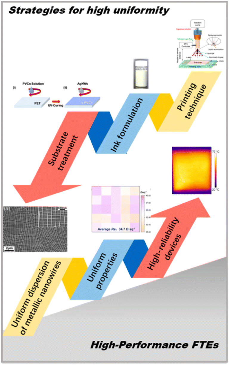 | ||
| Fig. 1 Schematic illustration of the importance of uniformity for high-performance FTEs. | ||
2 The influence of uniformity on the properties for FTEs
With the rapid development of wearable devices and artificial intelligence, flexible electronics have attracted more and more attention due to their potential for precise human–machine integration. However, before these applications can be realized, it is crucial to enhance the performance of FTEs. The most important properties for FTEs are optical and electrical properties; however, there is a trade-off between these two properties.41,42 When the areal mass density increases with more loading of metallic nanowires, the transmittance declines and the conductivity improves with more conductive pathways.43 In this section, we focus on the optical and electrical property improvement by fabricating metallic nanowire FTEs with high uniformity.2.1 Optical property
When light is directed through metallic nanowire FTEs, it undergoes adsorption, reflection, and transmission.44 The optical property of metallic nanowire FTEs refers to the percentage of transmitted light. The transmittance of the metallic nanowire network is related to the wavelength of light, and the transmittance at 550 nm is always used to evaluate the optical property of FTEs. Normally, the transmittance of metallic nanowire FTEs has a linear relationship with the amount of metallic nanowire on the films.44 Therefore, the dispersion of nanowires affects the uniformity of transmittance: areas where nanowires are densely stacked tend to have lower transmittance, while regions with lower nanowire density exhibit higher transmittance. Liu et al.45 prepared uniform copper nanowire (Cu NW) FTEs and examined the transparency in various spots. The as-prepared FTEs exhibited an average transmittance of 91.1% and the transmittance distribution varied from 89.5% to 92.0% even when the Cu NWs dispersion was homogenous. The transmittance was strongly related to the dispersion of nanowires in that the FTEs showed higher transparency with a higher open area.46 Therefore, nonuniformity, agglomeration, or segregation significantly affect the transparency of FTEs. Obvious clusters of metallic nanowires perhaps visible to human eyes is a fatal flaw for optoelectronic devices such as screens, LEDs, etc.2.2 Electrical property
The resistance of the metallic nanowire FTEs commonly includes the resistance in the nanowires themselves and the resistance between the adjacent nanowires, known as contact resistance or junction resistance. It's widely acknowledged that the conductivity of metallic nanowire FTEs is predominantly determined by the junction resistance.47–49 For example, the resistance of a single silver nanowire (Ag NW) was reported to be around 300 Ω, while the junction resistance between two Ag NWs was larger than 1 × 10⁹ Ω in comparison.50 Therefore, numerous methods have been reported to reduce the junction resistance of metallic nanowire networks, including thermal annealing,51,52 acid washing,53 light sintering,54–57 electro-induced welding,58,59 mechanical pressing,60 nanosoldering,29etc. The electrical conductivity of the metallic nanowire FTEs is affected by several factors, including the size,43,61 the areal mass density,62,63 the dispersion uniformity64 of metallic nanowires, etc. Among these factors, we focus on the function of uniformity on the conductivity of metallic nanowire FTEs.The uniformity of the FTEs is represented by a nonuniformity factor (NUF) to evaluate the standard deviation of sheet resistance from the average value as given below,65,66
 | (1) |
![[R with combining macron]](https://www.rsc.org/images/entities/i_char_0052_0304.gif) are the measured and average sheet resistances of all the measurements, respectively. A smaller value of NUF indicates a more uniform distribution of metallic nanowires on the substrate. Wang et al.67 systematically investigated the effects of the thickness of Ag NWs on the FTE properties and the results revealed that with the increase of the amount of Ag NWs, the sheet resistance and NUF of Ag NW FTEs decreased. Thus, it was difficult to achieve metallic nanowire FTEs with excellent conductivity and high uniformity, especially at high transparency. Chen et al.64 fabricated Ag NW FTEs with ultra-low haze and ultra-high uniformity by purifying Ag NWs with less nanoparticle containment. The achieved Ag NW FTEs showed good uniformity with a NUF of 5%. Fig. 2 shows the sheet resistance distribution of the Ag NWs in an area of 8 × 8 cm2. Owing to the small NUF, the Ag NW FTEs exhibited outstanding performance with a high transparency of 99.4% and a sheet resistance of 71.2 Ω sq−1. In comparison, spin-coated Ag NW FTEs affected by gradient Ag NW distribution had a much higher NUF of 101.1%.65
are the measured and average sheet resistances of all the measurements, respectively. A smaller value of NUF indicates a more uniform distribution of metallic nanowires on the substrate. Wang et al.67 systematically investigated the effects of the thickness of Ag NWs on the FTE properties and the results revealed that with the increase of the amount of Ag NWs, the sheet resistance and NUF of Ag NW FTEs decreased. Thus, it was difficult to achieve metallic nanowire FTEs with excellent conductivity and high uniformity, especially at high transparency. Chen et al.64 fabricated Ag NW FTEs with ultra-low haze and ultra-high uniformity by purifying Ag NWs with less nanoparticle containment. The achieved Ag NW FTEs showed good uniformity with a NUF of 5%. Fig. 2 shows the sheet resistance distribution of the Ag NWs in an area of 8 × 8 cm2. Owing to the small NUF, the Ag NW FTEs exhibited outstanding performance with a high transparency of 99.4% and a sheet resistance of 71.2 Ω sq−1. In comparison, spin-coated Ag NW FTEs affected by gradient Ag NW distribution had a much higher NUF of 101.1%.65
 | ||
| Fig. 2 (a) Well dispersed Ag nano-ink and a SEM image of Ag NW networks. (b) UV-vis curves of haze and transmittance vs. wavelength. (c) Optical image of the Ag NW FTE and its sheet resistance distribution. Reproduced with permission.64 Copyright 2017, the Royal Society of Chemistry. | ||
2.3 Stability
Metallic nanowire FTEs are prone to degradation under harsh or air environments due to the active features of metal. The failure mechanisms of Ag NW FTEs include exposure to corrosive gas in the atmosphere, Rayleigh instability induced by external heating or local Joule heating effects, and electromigration under electric field force.68,69 Among these failure modes, the degradation of metallic nanowire FTEs under current is considered to be strongly related to the uniformity of the metallic nanowire networks.Dorina et al.70 reported the failure of non-homogeneous Ag NW FTEs under electrical stress, demonstrating that the temperature distribution and the current density were strongly influenced by the non-homogeneities of Ag NW FTEs. This study indicated that the variations in conductivity resulted in degradation at hot spots due to current fluctuations, particularly in areas where the Ag NWs were thinner than others in the non-homogeneous FTEs. Wang et al.71 introduced chitosan-lactic acid (Chi-LaA) to Ag NW inks for fabricated FTEs with good uniformity and improved stability. After the addition of Chi-LaA, the Ag NWs dispersed homogenously, while the pristine Ag NWs formed obvious clusters, as shown in Fig. 3(a) and (b). As discussed in the above section, the optical and electrical properties were greatly affected by the dispersion of Ag NWs, as seen in the sheet resistance and transmittance of Ag NW FTEs with and without Chi-LaA given in Fig. 3(c) and (d). The Chi-LaA/Ag NW FTE exhibited more homogenous distribution thanks to the uniform Ag NW networks. Furthermore, the Ag NW FTEs with Chi-LaA exhibited improved stability in the ambient environment and improved thermal annealing and current stress compared with pure Ag NW FTEs. For example, the Ag NW FTE with Chi-LaA exhibited a much longer lifetime of 1272 h than that of pristine Ag NW FTEs under a DC current of 250 mA (Fig. 3(e)). The Chi-LaA inhibited the migration of Ag atoms under electrical stress, and the improved uniformity of Ag NWs eliminated the hot spots generated by Joule heating. The pristine Ag NW FTEs lost conductivity completely after only 10 h, while the sheet resistance of Chi-LaA/Ag NW FTEs increased from 16 to 48 Ω sq−1 after 20 h in contrast (Fig. 3(f)).
 | ||
| Fig. 3 The stability of the pristine Ag NW and uniform Chi-LaA/Ag NW FTEs. (a and b) Optical images. (c and d) Sheet resistance and transmittance of FTEs with a size of 6 × 6 cm2. (e) Resistance as a function of time under a current of 250 mA cm−2. (f) Sheet resistance as a function of time at high temperature of 180 °C. Reproduced with permission.71 Copyright 2020, the Royal Society of Chemistry. | ||
3 Engineering strategies for uniformity improvement
Metallic nanowire FTEs are usually fabricated by solution processes to achieve random conductive networks.72 Normally, there are three steps involved in the fabrication of metallic nanowire FTEs: synthesizing the metallic nanowires, printing them on flexible substrates, and post-treating the resulting films to improve their optoelectronic performance.37,38 The uniformity of the metallic nanowire networks strongly relies on the printing process, including the printing method and the states of the inks and substrates. In this part, we will discuss the strategies to fabricate homogeneous metallic nanowire FTEs by selecting appropriate printing techniques, adjusting the formulation of inks and employing substrate treatment methods.3.1 Printing technology selection
Metallic nanowires can be processed using solution methods, which are simpler and cheaper compared to complex physical methods. Various printing methods have been investigated to create random metallic networks, including drop coating, vacuum filtration, spin coating, spraying, and roll-to-roll printing.Drop coating involves directly dropping and drying liquid containing metallic particles on a substrate. The dried particles tend to assemble into a ring-like structure due to the “coffee ring effect”.73,74 As a result, films fabricated by the drop coating method often lack uniformity, which is undesirable in industrial applications.75 Layani et al.76 reported a fabrication process for uniformly patterned Ag FTEs utilizing the coffee ring effect. The dropped Ag nanoparticles formed a 2D array of interconnected rings with a width less than 10 μm. These arrays exhibited excellent performance, with a transparency of 95% and resistance of 0.5 Ω sq−1, which is better than commercial ITO. Zhang et al.77 also constructed conductive patterns with a 2D reticular structure based on the coffee ring effect on a hydrophilic glass substrate. The patterns exhibited high uniformity in which the randomly selected spots showed similar electrical conductivity. Although the drop coating method always leads to uneven dispersion of nanoparticles, uniform conductive patterns were achieved using the coffee ring effect by special design. Compared with drop coating, more uniform films can be formed using the vacuum filtration process.78,79 This method involves pumping the solvents through a filter and leaving the nanowires on the filter. Then, the nanowires are easily transferred to a flexible substrate without material waste.80,81 De et al.82 prepared Ag NW FTEs with the desired transparency by adjusting the thickness of Ag NWs using the vacuum filtration method. Ag NW FTEs with a sheet resistance of 13 Ω sq−1 and transmittance of 85% were successfully achieved. The films also showed high uniformity in which the transmittance varied less than 2% across different spots. Lyons et al.83 prepared thin networks of Au nanorods with high transparency and conductivity. The Au nanorods exhibited extreme uniformity on flexible substrates using the vacuum filtration method. Homogeneous Cu NW films have been prepared by the vacuum filtration method because the Cu NWs were coated with hydrophobic amine compounds, making the Cu NWs easily aggregate on PET or glass substrates using the normal drop coating method.58,84 Chu et al.53 demonstrated sintering-free Cu NW FTEs using a vacuum filtration coating process and pointed out that the vacuum filtration method was superior to other coating methods due to the wide selection of target substrates. In addition, the Cu NWs were firmly attached to the membrane filter during the vacuum filtration process, preventing unnecessary aggregation of the Cu NWs.85 The optical images in Fig. 4(a) illustrate the good uniformity of Cu NW FTEs prepared by vacuum filtration method.
 | ||
| Fig. 4 Printing techniques for uniform metallic nanowire FTEs. (a) Uniform Cu NW FTEs with different areal densities coated using vacuum filtration. Reproduced with permission.85 Copyright 2019, Elsevier. (b) Schematic representation of the one-probe electrical measurement (1-probe mapping) set-up and the 1-probe maps of Ag NW FTEs deposited via spray and spin coating processes. The left silver paste electrode is connected to ground, whereas 1.0 V is applied to the right silver paste electrode. The probe contacted the surface, and voltage was applied to measure the electric potential step by step. Reproduced with permission.86 Copyright 2018, American Chemical Society. (c) Sheet resistance of Ag NW FTEs using spray and spin coating methods as a function of storage duration. Reproduced with permission.87 Copyright 2015, the Royal Society of Chemistry. (d) Picture of the Ag NW FTEs prepared using a roll-to-roll method, and sheet resistance at different positions indicating good uniformity. Reproduced with permission.88 Copyright 2016, Nature Publishing Group. | ||
Although the vacuum filtration method is suitable for achieving homogenous metallic nanowire networks, it is not scalable. Spin coating and spraying are scalable techniques for coating metallic nanowires onto flexible substrates. Spin coating involves the deposition of nanowire suspension onto a flat substrate, followed by rapid rotation at high speeds to spread the nanowires uniformly across the surface through centrifugal force.89 This method is simple, cheap, and allows for precise control over the thickness of the nanowires by adjusting the spin speed and cycles.90 Shi et al.91 fabricated Ag NW FTEs using a two-stage spin coating process and the Ag NW films exhibited high transmittance and no obvious aggregation. Mayousse et al.87 reported that the spin-coated Ag NW FTEs on glass substrate exhibited an anisotropic orientation resulting in an electrode with low optoelectronic performance. In comparison, the spraying technique led to better performance by forming a randomly oriented mesh. As shown in Fig. 4(c), the Ag NW FTEs prepared by spray coating method exhibited higher transmittance with lower sheet resistance compared with those prepared by spin coating. Spraying requires a nozzle to spray the metallic nanowire suspension onto heated substrates to evaporated the solvent.54,55,92 Sannicolo et al.86 studied the impact of printing techniques on the electrical homogeneity of Ag NW FTEs using a 1-probe mapping method (Fig. 4(b)). The equipotential lines of the spin-coated FTE were non-isotropic and centripetally orientated due to the centrifugal force during the printing process. In contrast, the spray-coated FTE displayed parallel equipotential lines corresponding to a homogenous distribution of Ag NWs. Tao et al.93 fabricated highly uniform Ag NW conductors on paper substrates through an optimized spraying process with the proper spraying path and parameters. The NUF was reduced to below 10% and even 5% under certain conditions. Chu et al.52 reported the preparation of large-area (>50 cm2) Cu NW FTEs by the low-cost spraying method, and the Cu NWs partially fused due to the high kinetic energy during the spray deposition process. Thus, the uniform Cu NW FTE exhibited high performance with a transmittance of 90% and sheet resistance of 52.7 Ω sq−1. The spraying method is an efficient printing method to achieve uniform networks and is suitable for scalable production on flat or curved substrates.
The roll-to-roll method is a typical printing process for mass production and always integrates with a post treatment process to form an assembly line.94,95 Kim et al.88 printed a 400 mm wide Ag NW FTEs using a continuous roll-to-roll slot die coating process to make large-area flexible touch screen panels. The resistance of the Ag NW FTEs was measured along the width direction to evaluate the uniformity of Ag NWs, and the results demonstrated that the resistance had a small fluctuation around 50 Ω sq−1 (Fig. 4(d)). The dispersion of Ag NWs is related to the physical properties of the ink (viscosity and tension) and the feeding of the substrate during the roll-to-roll coating process.94,96 Therefore, the uniformity of the metallic nanowires can be optimized by adjusting the properties of the nanowires and substrates, which will be introduced in the following sections.
Beyond the conventional printing techniques, there are specialized structural designs for uniform metallic networks using self-assembly methods.97–99 Duan et al.100 reported a water-bath assisted convective assembly process to fabricate hierarchically aligned Ag NW FTEs. A uniform Ag NWs grid structure was formed simply by several dip-coating cycles under the function of convection flow. Thanks to the ordered structure, the roughness of the as-prepared Ag NW FTEs was lower than that of spin coating films, which is helpful for the application of FTEs in photoelectric devices. Han et al.8 realized large-area Ag NW FTEs with desired patterns through a 2D ice-templating approach. The Ag NW FTE achieved a high transmittance of 91% and low sheet resistance of 20 Ω sq−1. Yang et al.101 fabricated Ag NW FTEs with an ordered network structure using interface assembly and wetting induced climbing transfer process. The ordered Ag NW FTEs exhibited a uniform grid structure (Fig. 5(a)) and the surface roughness, sheet resistance and transparency showed higher uniformity than the random Ag NW networks. Thanks to the highly ordered structure, the Ag NW FTEs showed remarkable performance, with a sheet resistance of 10.6 Ω sq−1 and transmittance of 96%. Cho et al.102 demonstrated a bar-coating assembly technique for the fabrication of cross-aligned Ag NW FTEs with sheet resistance of 21 Ω sq−1 at 95% transparency. The cross-aligned Ag NW FTEs showed a uniform distribution of sheet resistance with a small deviation of 1.2 due to the ordered geometry of the Ag NW networks and uniform nanowire–nanowire junctions, as shown in Fig. 5(b). Likewise, the transmittance distribution of the cross-aligned Ag NW FTEs showed a better uniformity with a standard deviation of 0.3 in comparison to the deviation for random Ag NW FTE of 0.8. Feng et al.103 also presented a cost-effective strategy to prepare aligned Ag NW FTEs with excellent uniformity. The as-fabricated Ag NW FTEs exhibited an ultrahigh transmittance of 99.1% and sheet resistance of 91 Ω sq−1 with a low areal mass density of only 8.3 mg m−2. In comparison, the random Ag NW FTEs exhibited a sheet resistance of 228.3 Ω sq−1 and a transmittance of 94%.104
 | ||
| Fig. 5 Comparison of ordered and random Ag NW FTEs. (a) SEM images, AFM height profile, sheet resistance distribution. Reproduced with permission.101 Copyright 2024, Wiley-VCH. (b) Photograph of large scale (20 × 20 cm2) FTE and the mapping showing the distribution of sheet resistance and transmittance for the cross-aligned and random Ag NW FTEs. Reproduced with permission.102 Copyright 2017, American Chemical Society. | ||
From the above introduction, the vacuum filtration and spraying methods are excellent techniques to fabricate uniform metallic nanowire FTEs on various substrates. The performance of the metallic nanowire FTEs strongly depends on the uniformity of the nanowires. We summarize the selection of printing method for different applicable uses in Table 1.
| Methods | Advantages | Disadvantages | Applications |
|---|---|---|---|
| Drop coating | Simple | Nonuniform | Devices with low uniformity requirements, e.g. flexible conductive track |
| Low cost | |||
| Vacuum filtration | Uniform | Not applicable to large areas | Small size device, e.g., OLEDs, SCs, ECDs |
| Ink-saving | |||
| Strong controllability | |||
| Spin coating | Simple | Ink-wasting | e.g. OLEDs, SCs, ECDs |
| Spraying | Compatible with non-planar transparent substrates | Weak controllability | Almost all areas, especially for non-planar electronics, e.g. curved displays |
| Ink-wasting | |||
| Roll-to-roll | Large-scale production | Expensive equipment | Commercial mass production |
3.2 Improvement of ink formulation
To achieve homogenous metallic nanowire FTEs, the uniformity of the printing inks is crucial. However, the metallic nanowires easily agglomerate or precipitate in solvent during storage. Aggregated metallic nanowires will cause bad uniformity. Some techniques have been employed to prevent the agglomeration of metallic nanowires through surface modification of nanowires or selecting proper additives.The surface properties of the metallic nanowires can be chemically modified via ligand exchange reactions, which can improve the uniform distribution of metallic nanowires in the polymer matrix.106 Choi et al.107 fabricated stretchable heaters made of homogeneous Ag NWs in styrene-butadiene-styrene elastomer. The original polyvinylpyrrolidone (PVP) on the Ag NWs was changed to hexylamine to improve the dispersion of Ag NWs in the polymer. The well-dispersed Ag NWs network increased the conductive paths and exhibited an enhanced conductivity. Lu et al.108 presented a stretchable conductor using surface-modified Ag NWs and thermoplastic PU. The Ag NWs after surface modification were well dispersed in PU polymer and had enhanced electrical property due to the homogenous network.
For Cu NWs, the synthesis process always involves linear alkyl amines as the surfactant, as they are water insoluble and hydrophobic.35 However, the commonly used substrates for FTEs are hydrophilic glass, PET or PEN, etc. As mentioned above, Cu NWs with hydrophobic surfactants easily aggregate on substrates during the printing process. Li et al.51 obtained well dispersed PVP-capped Cu NWs via a ligand exchange method and prepared Cu NW FTEs with excellent properties (30 Ω sq−1 at 86% transmittance) using a spin coating process. Liu et al.45 prepared high-performance Cu NW FTEs using a pickling-chemical sintering approach at room temperature. The Cu NWs were pickled to remove the hydrophobic oleylamine and uniform Cu NWs FTEs were achieved, showing homogeneous photoelectric properties in an area of 5 × 5 cm2. Zhong et al.109 fabricated Cu NW FTEs with high uniformities using surface modified Cu NWs inks in isopropyl alcohol (IPA). The Cu NWs capped with hexadecylamine (HDA) surfactant were poorly dispersed in polar IPA. To improve the dispersion, the surfactant on the Cu NWs was changed to PVP by a ligand exchange process (Fig. 6). The Cu NW FTEs prepared with the ligand exchanged Cu NWs showed good electrical and optical uniformity. The large-area Cu NW FTE exhibited an average sheet resistance of 24.5 Ω sq−1 with a small deviation of 1.9 Ω sq−1 and average transmittance of 83% with a deviation of 1.1%. From the above, we can conclude that the Cu NWs with hydrophobic surfactants are usually modified by a ligand exchange process to improve the dispersion in polar solvent and further enhance the uniformity on substrates, especially when using the drop coating, spin coating or roll-to-roll coating methods.
 | ||
| Fig. 6 Surface modification of Cu NWs for uniform FTEs. (a) Schematic illustration of the ligand exchange process for highly dispersed Cu NW ink. (b) Photograph of large-scale (150 × 200 mm2) Cu NW FTE divided into 16 zones to characterize its sheet resistance (center) and transmittance (right) uniformity. Reproduced with permission.109 Copyright 2016, the Royal Society of Chemistry. | ||
In short, surfactants such as PVP used during the synthesis of metallic nanowires effectively prevent agglomeration and enhance uniformity. Therefore, by modifying the surface of nanowires with appropriate surfactants depending on the solvent used for dispersion, excellent uniformity can be achieved, laying a solid foundation for the fabrication of highly uniform FTEs.
Wang et al.71 introduced Chi-LaA to Ag NW aqueous solution to improve the dispersion of Ag NW ink. Highly uniform and stable Ag NW FTEs were achieved with a NUF of 7%. In comparison, the NUF of Ag NW FTEs prepared with aqueous ink was as high as 49%, demonstrating poor uniformity. From the optical and infrared images in Fig. 7(a), after the addition of Chi-LaA, the Ag NWs exhibited high uniformity in the whole area. The Ag NWs were agglomerated into clusters and exhibited uneven heating property without Chi-LaA. Sun et al.111 reported high-performance Ag NW FTEs with a sheet resistance of 10 Ω sq−1 and a transmittance of 92% using water-processed Ag NWs and poly(sodium 4-styrenesulfonate) (PSSNa) as a polyelectrolyte. Relying on the electrostatic charge repulsion caused by the PSSNa on the Ag NWs, the ink was homogeneous and stable. The as-prepared Ag NW FTEs exhibited higher uniformity compared with those without PSSNa with similar Ag NW coverage, as shown in Fig. 7(b). Various polyelectrolytes were used in this report including neutral PVA, PVP, PEO and negative PAAS, but these positive electrolytes did not offer the improved performance of the Ag NW FTES with PSSNa. Chen et al.113 reported a suitable agent (cellulose nanofibril (CNF)) to promote the uniformity of Ag NW FTEs and revealed that the CNF dramatically enhanced the Ag NW dispersity and optimized the drying process. The conductivity and uniformity were promoted. The zeta potential was much higher with 0.25 wt% CNF, indicating a large electrostatic repulsion among Ag NWs; thus, the dispersion of Ag NWs was greatly promoted. Chen et al.112 proposed a wet film leveling process for promoting the uniformity of Ag NW FTEs, as shown in Fig. 7(c). The leveling agent eliminated the surface tension gradient and led to a flat surface through the reflow process of wet film. When n-pentanol was selected as the leveling agent, the sheet resistance and corresponding variation coefficient of the Ag NW FTEs decrease from 38.3 Ω sq−1/3.83% to 25.7 Ω sq−1/1.88%. Chen et al.110 explored several additives to promote the whole printing process, including the dispersion of Ag NWs and the wetting and drying processes of the films. 2-Amino-2-methyl-1-propanol was used to reduce the aggregation of the Ag NWs by strengthening the repulsive force between Ag NWs. Zonyl FSO-100 adjusted the surface tension to endow excellent wettability of the ink on substrates. Diacetone alcohol was used as a leveling regent to obtain flat films. Using the as-prepared Ag NW ink, a uniform and large-scale FTE (0.5 × 10 m2) was printed by a roll-to-roll process and applied on a touch screen.
 | ||
| Fig. 7 Selecting proper additives in metallic nanowire inks. (a) Fabrication process for Ag NW FTEs with Chi-LaA addition (left); SEM image and infrared thermal images of pristine and Chi-LaA modified Ag NW FTEs. Reproduced with permission.71 Copyright 2020, the Royal Society of Chemistry. (b) SEM images of the Ag NW FTEs prepared from the pristine Ag NW suspension and with PSSNa. Reproduced with permission.111 Copyright 2019, Nature Publishing Group. (c) The schematic and sheet resistance distribution of Ag NW FTEs without and with wet film leveling process; the mean value and standard deviations of sheet resistance of Ag NW FTEs with different additions of leveling agent. Reproduced with permission.112 Copyright 2024, the American Chemical Society. | ||
3.3 Surface treatment of substrates
According to the Young equation,114 when the surface tension of the metallic nanowire ink is higher than that of the substrate, the ink exhibits bad wettability. Then, the metallic nanowires cannot disperse uniformly on the substrates. In general, to achieve good wettability, adjusting the ink formulation or modifying the surface of the substrate are effective methods.115 By tuning the properties of substrate and printing ink, it is possible to achieve metallic networks with different structures by changing the capillary force between the ink and substrates.116 The commonly used substrates for metallic FTEs are glass, PET, PEN, PI, PDMS, PU, etc. Unfortunately, metallic nanowires in organic solvent are not able to disperse uniformly on these substrates without further treatment. Thus, surface treatment or coating with an underlying layer is another strategy to improve the dispersion of metallic nanowires during the coating process.117The hydrophilic property of the PET, PEN or PI substrates can be improved by plasma treatment.118 For example, the contact angle of water on PET decreased from 84.5° to 34.6° after air plasma treatment.119 The decrease of contact angle revealed the improved hydrophily of PET substrates, which benefits the metallic nanowire dispersion during the printing process. Wu et al.120 prepared Ag NW FTEs on pre-treated PET substrate and achieved uniform Ag NW networks by a simple drop casting process. Moon et al.121 produced large scale, high-performance Ag NW/GO FTEs on PET substrates. To improve the dispersion of Ag NWs on PET substrates, the PET surface was treated with O2 plasma to reduce the water contact angle from 62.37° to 15.14°. The as-prepared Ag NW/GO FTE exhibited superior properties, including high conductivity (24.8 Ω sq−1), high transparency (92%), high durability under bending, good chemical stability, and high electrical uniformity. The sheet resistance deviated only 1.07% from the average value of 24.8 Ω sq−1 for a large-area FTE with size of over 50 mm2.
Beyond plasma treatment, hydrophilic polymers or materials have been designed to coat the original substrates as an underlying layer to improve the wetting and adhesion of metallic nanowires on the flexible substrates. Akter et al.122 prepared stretchable Ag NW FTEs on polydopamine modified PDMS substrates. The contact angle for PDMS was 115° and it was difficult to disperse hydrophilic Ag NWs on the highly hydrophobic PDMS. The contact angle declined to 25.7° after polydopamine modification and the Ag NWs were evenly distributed on the treated surface. The creation of a hydrophilic surface is important for the printing of uniform Ag NW films. Kim et al.115 demonstrated a patterned Ag NW FTE prepared using the photolithography method. Before coating the Ag NWs on a PET substrate, a cross-linked poly(vinyl cinnamate) (x-PVCn) film was introduced as the underlayer to improve the uniformity and adhesion. As shown in Fig. 8(a), the Ag NW FTEs on untreated PET exhibited poor uniformity and the sheet resistance varied from 14 Ω sq−1 to more than 100 Ω sq−1. In comparison, the Ag NW FTEs on x-PVCn coated PET showed good homogeneity with a sheet resistance of 29.5 ± 7.2 Ω sq−1. Kwon et al.123 prepared high-performance Ag NW FTEs on a surface treated PEN substrate using poly(2-hydroxyethyl methacrylate) (PHEMA) as an underlayer. The contact angle of PEN was reduced from 84.2° to 46.5° after the surface coating of PHEMA, showing much better hydrophilic property, as shown in Fig. 8(b). Ag NWs with hydrophilic PVP on the surface were distributed more uniformly than on the original hydrophobic PEN. Graphene oxide (GO) has also been used as the underlayer to improve the uniformity of Ag NWs on flexible substrates. Naito et al.124 prepared GO/Ag NW/GO composite FTEs on PET substrate. On the underlayer GO, Ag NWs dispersed uniformly with a small sheet resistance deviation because GO has many hydrophilic hydroxyl and carboxyl functional groups. Li et al.125 prepared high-performance FTEs consisting of Ag NWs and poly(diallyldimethyl-ammonium chloride) (PDDA) with a layer-by-layer assembled structure. In this study, the surface treatment of PET with PDDA played an essential role in the FTE fabrication process. The Ag NWs exhibited obvious aggregation on the O2 plasma-treated PET substrate without PDDA modification. In comparison, the Ag NWs dispersed uniformly on the PDDA modified PET substrate thanks to the strong electrostatic interactions between PDDA and Ag NWs. The Ag NWs and PDDA composite FTEs showed outstanding performance with a sheet resistance of 12.3 Ω sq−1 at 91.7% transmittance, which was much better than those of pure Ag NW FTEs (184 Ω sq−1 at 88% transmittance) due to the uniform Ag NW network with small variations at different locations.
 | ||
| Fig. 8 The substrate treatment or coating for uniform dispersion of metallic nanowires. (a) Optical images and sheet resistance distribution of Ag NW based FTEs on bare PET and the x-PVCn coated PET substrate. Reproduced with permission.115 Copyright 2020, American Chemical Society. (b) Contact angle and optical images of Ag NW FTEs on PEN and PHEMA coated PEN substrates. Reproduced with permission.123 Copyright 2022, American Chemical Society. | ||
In brief, by controlling the surface state of the substrate, different morphologies of metallic nanowire networks can be obtained. Metallic nanowire inks often exhibit poor wettability on common substrates such as glass, PET, and PEN. Therefore, plasma treatment or the application of modifying materials can be used to improve the wettability of nanowires on these substrates, resulting in highly uniform FTEs.
To sum up, the uniformity of the metallic nanowire FTEs has been improved using the mentioned strategies, mainly selecting printing techniques, adjusting the ink formulation, and treating the surface of substrates. There are also some other factors that affect the uniformity of the metallic nanowires, but have not been sufficiently studied in previous papers. For example, the morphology and distribution of the Ag NW network was different at various concentrations. When the Ag NW ink was 4 mg mL−1, the Ag NW FTEs exhibited better uniformity.111 The drying process of the conductive ink can be adjusted by heating processes.126 Jia et al.65 reported a dynamic heating process to achieve Ag NW FTEs with high uniformity. The dynamic heating method overcomes the coffee ring effect by adjusting the drying process of the wet film. The NUF of the Ag NW FTE was as low as 6.7%, which was comparable to those of commercial ITO films. The previous achievements for uniform metallic nanowire FTEs are summarized and compared in Table 2.
| Materials | Printing methods | Transmittance (%) | Sheet resistance (Ω sq−1) | NUF (%) | Ref. no |
|---|---|---|---|---|---|
| Cu NWs | Meyer rod | 91.1 | 34.7 | — | 45 |
| Ag NWs | Spray coating | 80 | 10 | — | 47 |
| Cu NWs | Spray coating | 90 | 52.7 | — | 52 |
| Cu NWs | Spray coating | 78 | 22.1 | — | 55 |
| Ag NWs | Vacuum filtration | 91.7 | 71.2 | 5 | 64 |
| Ag NWs | Spin coating | 95.5 | 35 | 6.7 | 65 |
| Ag NWs | Meyer rod | 90 | 38 | ∼0.53 | 67 |
| Ag NWs | Meyer rod | 91.9 | 21 | 7 | 71 |
| Ag NWs | Drop coating | 95 | 0.5 | — | 76 |
| Ag NWs | Spray coating | ∼20 | — | <10 | 93 |
4 Applications
4.1 Effects of uniformity on transparent heaters (THs)
Transparent heaters (THs) are one of the most common and structurally simple devices based on FTEs.127–129 They have found widespread applications in various fields, such as transportation, construction, and healthcare, where they are used as smart windows,130–132 de-icing devices,133–135 defoggers,136,137 thermal therapy pads,138–140 and more. THs typically consist of a two-layer structure: a transparent substrate layer at the bottom and a conductive layer on top (Fig. 9(a)). Additionally, a transparent encapsulation layer can be optionally coated to the surface to provide protection.140 When a current passes through the conductive layer, heat (Q) is generated according to Joule's Law,144,145 | (2) |
 | ||
| Fig. 9 The effect of FTE uniformity on heating performance. (a) Schematic illustration of the transparent heater.141 Copyright 2020, Wiley-VCH. (b) Uneven temperature distribution caused by a nonuniform electrode. Reproduced with permission.142 Copyright 2013, Wiley-VCH. (c) The change in resistance and maximum temperature on a Ag NW network sample with an initial resistance of 8.9 Ω when applying a voltage ramp. (d) The damage of Ag NWs caused local overheating and the infrared image of the crack beginning from the green hot spots. Reproduced with permission.143 Copyright 2021, the Royal Society of Chemistry. | ||
4.2 Effects of uniformity on solar cells (SCs)
Solar cells are devices that directly convert light energy into electrical energy through the photovoltaic effect or photochemical effect.149–151 The electricity generated by solar cells is clean and harmless, producing no pollution or carbon dioxide emissions. Therefore, they play a positive role in mitigating climate change, improving air quality, and protecting the environment.152–154 Although conventional rigid silicon-based solar cells currently dominate the commercial market, emerging technologies, such as organic SCs (OSCs) and perovskite SCs (PSCs), with the compatibility of flexibility, solution processability, and broad spectral response, have attracted increasing attention.155–158 Typically, the OSCs or PSCs contain five layers: TE (including transparent substrate and conductive layer), electron transport layer, photosensitive layer (e.g., poly(3-hexylthiazol), perovskite), hole transport layer and metallic electrode.159 Clearly, non-uniformity of the TE would directly lead to uneven absorption of light energy, as well as uneven collection and transport of electrons, thereby diminishing the overall PCE. Furthermore, the deterioration of electrical performance caused by Joule heat during SCs' operation reduces the lifespan of the entire device. Although the current density generated in OSCs is relatively low (on the order of about 10 mA cm−2), the current density generated in NWs is very high. For instance, if we assume that a NW TE with conductivity of 12 Ω sq−1 participates in current conduction, then a current density of 17 mA cm−2 in the solar cell would result in an approximate current density of 4 × 10⁷ mA cm−2 in the NWs (i.e., current passing through a single nanowire divided by its cross-sectional area).69 Such high current stress would cause the “avalanche effect” and make the whole SC fail. Additionally, the large surface roughness caused by the uneven distribution of NWs can also lead to the failure of SCs. Moreover, low surface roughness can reduce light scattering and enhance the light utilization efficiency.160 On the other hand, the large surface roughness caused by the nonuniform distribution of NWs can make the device prone to breakdown and short-circuit failures.274.3 Effects of uniformity on electrochromic devices (ECDs)
Electrochromic devices (ECDs), with the ability to reversibly adjust optical properties, have found widespread applications in various fields, such as smart windows for buildings,161,162 displays,163–165 and sensing,166–168 attracting considerable attention from both industry and academia. These devices typically consist of a five-layer structure, with top and bottom layers comprised of transparent electrodes made of transparent substrates and conductive layers, respectively, onto which electrochromic layers and counter electrode layers are deposited to achieve color-changing functionality and ion storage during this process. Sandwiched between them is an electrolyte layer for ion transport.169 Clearly, transparent electrodes are one of the key components for applying electric fields to the electrochromic materials. Firstly, the nonuniformity of transparent electrodes can result in non-uniform distribution of electric fields in the active layer, thereby affecting the optical uniformity of the device.170 In the investigation of zinc-based electrochromic devices, Li and colleagues171 found that placing metallic zinc on only one side of the device leads to an uneven distribution of electric fields on the opposite ITO electrode surface, causing inconsistencies in the coloring process (Fig. 10(a)). Hu et al.173 effectively improved the uniformity of the electric field by introducing a copper mesh within the flexible ITO electrode, achieving a more uniform coloring process (Fig. 10(c)). Secondly, the uneven distribution of conductive materials can result in nonuniform coating of electrochromic materials. Research conducted by Zhang et al.172,174 suggests that the nonuniformity of nanowire-based electrodes led to uneven electrodeposition of polyaniline electrochromic materials, resulting in excessive coloring in specific localized areas (Fig. 10(b)). Thirdly, the uniformity of transparent electrodes also affects the stability of the device: the uneven coloring is essentially an uneven state of oxidation–reduction reactions. Excessive oxidation or reduction in localized areas can lead to a decrease in the device's lifespan. Moreover, as mentioned above, locally elevated temperatures and high roughness resulting from a non-uniform electrode distribution can also lead to device failure. | ||
| Fig. 10 The effect of FTE uniformity on electrochromic performance. (a) Electric field distribution of Zn-based ECD while placing a metallic zinc electrode on only one side. Reproduced with permission.171 Copyright 2020, Wiley-VCH. (b) Nonuniform colored state caused by the uneven deposition of polyaniline electrochromic materials. Reproduced with permission.172 Copyright 2021, Elsevier. (c) Improved uniformity of electric field distribution and electrochromic process by introducing copper mesh onto ITO FTE. Reproduced with permission.173 Copyright 2022, Wiley-VCH. | ||
5 Conclusion
Traditional ITO has been the primary choice for transparent electrodes for decades in rigid electronics and continues to hold its position due to its exceptional properties and reliability across various applications, including touch screens, SCs, LEDs and ECDs. However, with the evolution of electronics, flexible or wearable electronics must be raised up to meet the desires of modern life with convenience and intelligence. Metallic nanowires represent a promising alternative to ITO, particularly for flexible electronics, owing to their impressive optoelectronic performance and inherent flexibility. Extensive research efforts have been dedicated to developing fabrication techniques and structural designs for high-performance metallic nanowire FTEs. Prior to deployment, it is imperative to ensure the uniformity and reproductivity of the metallic nanowire FTEs to meet stringent production quality standards.Given the importance of uniformity for the metallic nanowire FTEs, it is essential to explore strategies for optimizing the uniform dispersion of metallic nanowires on flexible substrates. In this review, we discussed how the dispersion of metallic nanowires influences the optical and electrical properties and stability of the FTEs. Remarkable advancements have been made in developing suitable printing techniques for nano-inks, exchanging surfactants, and selecting proper additives to modify the ink formulation, and diverse techniques to improve the substrate wettability have been reviewed to realize highly uniform metallic nanowire FTEs. Moreover, the performance of flexible devices, including FTs, SCs and ECDs integrated with uniform FTEs, has been introduced. The importance of this review lies in providing a system for understanding the importance of the uniformity of metallic nanowires for the properties and applications of FTEs.
Despite the importance of the uniformity for metallic nanowire FTEs having been recognized and studied, the existing literature on this topic is still relatively limited, and significant challenges remain in achieving uniform metallic nanowire FTEs in high-quality production lines. For example, 1D metallic nanowires tend to precipitate in solution or even form clusters during storage, posing challenges in achieving homogeneous networks using uneven nano-inks. Additionally, ensuring the stability of metallic nanowires in various environments remains an important challenge for flexible FTEs. Although many methods have been reported to protect metallic nanowires, they are still susceptible to inevitable exposure to the air, high temperatures or electrical fields.
Flexible electronics are gaining increasing attention, and FTEs as an essential component have also been researched intensely. Continuing efforts in both fundamental study and application exploration are essential for the development of flexible electronics. Thanks to the current intensive research on metallic nanowire FTEs, we hope the era of flexible devices will soon become part of everyday life for humans.
Data availability
No primary research results, software or code have been included and no new data were generated or analysed as part of this review.Conflicts of interest
There are no conflicts to declare.Acknowledgements
The authors are grateful for financial support from State Key Laboratory of Advanced Welding and Joining (AWJ-23M20).References
- J. Jinwook Kim, S. Kojima, J. Zheng, X. He, A. Sajjad, H. Zhang, H. Su and W. C. H. Choy, Nat. Commun., 2024, 15, 2070 CrossRef PubMed.
- S. Luo, E. Lian, J. He and J. C. deMello, Adv. Mater., 2023, 2300058 Search PubMed.
- B. Sun, R. Xu, X. Han, J. Xu, H. Wang, Y. Xu, Z. Fu, Z. He, X. Sun, J. Wang, P. Cui, J. Chang, J. Xiong and K. Qian, npj Flexible Electron., 2022, 6, 48 CrossRef CAS.
- T. Cheng, X. L. Yang, S. Yang, L. Li, Z. T. Liu, J. Qu, C. F. Meng, X. C. Li, Y. Z. Zhang and W. Y. Lai, Adv. Funct. Mater., 2023, 33, 2210997 CrossRef CAS.
- S. Yu, J. Li, L. Zhao, B. Gong and L. Li, Sol. Energy Mater. Sol. Cells, 2021, 231, 111323 CrossRef CAS.
- M. Li, W. W. Zuo, A. G. Ricciardulli, Y. G. Yang, Y. H. Liu, Q. Wang, K. L. Wang, G. X. Li, M. Saliba, D. Di Girolamo, A. Abate and Z. K. Wang, Adv. Mater., 2020, 32, e2003422 CrossRef PubMed.
- K. Zilberberg and T. Riedl, J. Mater. Chem. A, 2016, 4, 14481–14508 RSC.
- J. Han, J. Yang, W. Gao and H. Bai, Adv. Funct. Mater., 2021, 31, 2010155 CrossRef CAS.
- X. L. Duan, Y. Ding and R. Y. Liu, Mater. Today Energy, 2023, 37, 101409 CrossRef CAS.
- V. H. Nguyen, D. T. Papanastasiou, J. Resende, L. Bardet, T. Sannicolo, C. Jiménez, D. Muñoz-Rojas, N. D. Nguyen and D. Bellet, Small, 2022, 18, 2106006 CrossRef CAS.
- J. Lewis, S. Grego, B. Chalamala, E. Vick and D. Temple, Appl. Phys. Lett., 2004, 85, 3450–3452 CrossRef CAS.
- K. Rana, J. Singh and J.-H. Ahn, J. Mater. Chem. C, 2014, 2, 2646–2656 RSC.
- J. L. Sun, Y. Chang, J. Liao, S. L. Chang, S. G. Dai, Y. Y. Shang, C. X. Shan and L. Dong, Nano Energy, 2022, 99, 107392 CrossRef CAS.
- M. Kauk-Kuusik, K. Timmo, M. Pilvet, K. Muska, M. Danilson, J. Krustok, R. Josepson, V. Mikli and M. Grossberg-Kuusk, J. Mater. Chem. A, 2023, 11, 23640–23652 RSC.
- K. Fukuda and T. S. Kilho Yu, Adv. Energy Mater., 2020, 10, 2000765 CrossRef CAS.
- C. Xie, Y. Liu, W. X. Wei and Y. H. Zhou, Adv. Funct. Mater., 2023, 33, 2210675 CrossRef CAS.
- H. Liu, X. T. Yi, J. Wu, Y. Z. Li, H. Tang, Z. G. Li, Y. Y. Fu and Z. Y. Xie, Mater. Sci. Semicond. Process., 2024, 173, 108113 CrossRef CAS.
- H. Zhang, F. Sun, J. Feng, H. Ling, D. Zhou, G. Cao, S. Wang, F. Su, Y. Tian and Y. Tian, Cell Rep. Phys. Sci., 2022, 3, 101193 CrossRef CAS.
- H. Zhang, F. Sun, G. Cao, D. Zhou, G. Zhang, J. Feng, S. Wang, F. Su, Y. Tian and Y. J. Liu, Int. J. Extreme Manuf., 2023, 5, 015503 CrossRef CAS.
- H. Gong, A. Li, G. X. Fu, M. Y. Zhang, Z. L. Zheng, Q. Q. Zhang, K. L. Zhou, J. B. Liu and H. Wang, J. Mater. Chem. A, 2023, 11, 8939–8949 RSC.
- Y. F. Ding, H. H. Sun, Z. H. Li, C. M. Jia, X. G. Ding, C. Li, J. G. Wang and Z. Li, J. Mater. Chem. A, 2023, 11, 2868–2875 RSC.
- J. Yun, Y. H. Park, T. S. Bae, S. Lee and G. H. Lee, ACS Appl. Mater. Interfaces, 2013, 5, 164–172 CrossRef CAS PubMed.
- A. M. Bazargan, F. Sharif, S. Mazinani and N. Naderi, J. Mater. Sci.: Mater. Electron., 2017, 28, 2962–2969 CrossRef CAS.
- K.-H. Choi, J.-A. Jeong, J.-W. Kang, D.-G. Kim, J. K. Kim, S.-I. Na, D.-Y. Kim, S.-S. Kim and H.-K. Kim, Sol. Energy Mater. Sol. Cells, 2009, 93, 1248–1255 CrossRef CAS.
- Y. Shen, Z. Feng and H. Zhang, Mater. Des., 2020, 193, 108809 CrossRef CAS.
- Y. Yang, B. Xu and J. Hou, Chin. J. Chem., 2021, 39, 2315–2329 CrossRef CAS.
- M.-R. Azani, A. Hassanpour and T. Torres, Adv. Energy Mater., 2020, 10, 2002536 CrossRef CAS.
- H. Zhang, Y. Tian, S. Wang, Y. Huang, J. Wen, C. Hang, Z. Zheng and C. Wang, Chem. Eng. J., 2020, 399, 125075 CrossRef CAS.
- Y. Huang, Y. Tian, C. Hang, Y. Liu, S. Wang, M. Qi, H. Zhang and J. Zhao, ACS Appl. Mater. Interfaces, 2019, 11, 21850–21858 CrossRef CAS PubMed.
- S. H. Pham, A. Ferri, A. D. Costa, M. M. S. Mohan, V. D. Tran, D. C. Nguyen, P. Viville, R. Lazzaroni, R. Desfeux and P. Leclère, Adv. Mater. Interfaces, 2022, 9, 2200019 CrossRef CAS.
- M. Singh and S. Rana, Mater. Today Commun., 2020, 24, 101317 CrossRef CAS.
- H. Zhang, S. Wang, Y. H. Tian, Y. B. Liu, J. Y. Wen, Y. L. Huang, C. J. Hang, Z. Zheng and C. X. Wang, Chem. Eng. J., 2020, 390, 124495 CrossRef CAS.
- S. Wang, Y. Tian, C. Hang and C. Wang, Sci. Rep., 2018, 8, 5260 CrossRef PubMed.
- D. Chen, F. Zhao, K. Tong, G. Saldanha, C. Liu and Q. Pei, Adv. Electron. Mater., 2016, 2, 1600167 CrossRef.
- S. Zhao, F. Han, J. Li, X. Meng, W. Huang, D. Cao, G. Zhang, R. Sun and C. P. Wong, Small, 2018, 14, 1800047 CrossRef PubMed.
- S. Ding and Y. Tian, RSC Adv., 2019, 9, 26961–26980 RSC.
- S. Ye, A. R. Rathmell, Z. Chen, I. E. Stewart and B. J. Wiley, Adv. Mater., 2014, 26, 6670–6687 CrossRef CAS PubMed.
- T. Sannicolo, M. Lagrange, A. Cabos, C. Celle, J. P. Simonato and D. Bellet, Small, 2016, 12, 6052–6075 CrossRef CAS PubMed.
- V. Rai, R. S. Singh, D. J. Blackwood and Z. L. Dong, Adv. Eng. Mater., 2020, 22, 2000082 CrossRef CAS.
- D. Won, J. Bang, S. H. Choi, K. R. Pyun, S. Jeong, Y. Lee and S. H. Ko, Chem. Rev., 2023, 123, 9982–10078 CrossRef CAS PubMed.
- G. Milano, A. Cultrera, K. Bejtka, N. De Leo, L. Callegaro, C. Ricciardi and L. Boarino, ACS Appl. Nano Mater., 2020, 3, 11987–11997 CrossRef CAS.
- M. Lagrange, D. P. Langley, G. Giusti, C. Jiménez, Y. Bréchetef and D. Bellet, Nanoscale, 2015, 7, 17410–17423 RSC.
- R. M. Mutiso, M. C. Sherrott, A. R. Rathmell, B. J. Wiley and K. I. Winey, ACS Nano, 2013, 7, 7654–7663 CrossRef CAS PubMed.
- A. R. Rathmell and B. J. Wiley, Adv. Mater., 2011, 23, 4798–4803 CrossRef CAS PubMed.
- Q. Liu, Y. Wu, Y. Li, Y. Shi, Q. Pan, D. Yang and T. Wang, Chem. Eng. J., 2023, 472, 145030 CrossRef CAS.
- M. Marus, A. Hubarevich, H. Wang, Y. Mukha, A. Smirnov, H. Huang, W. Fan and X. W. Sun, Thin Solid Films, 2017, 626, 140–144 CrossRef CAS.
- E. C. Garnett, W. Cai, J. J. Cha, F. Mahmood, S. T. Connor, M. Greyson Christoforo, Y. Cui, M. D. McGehee and M. L. Brongersma, Nat. Mater., 2012, 11, 241–249 CrossRef CAS PubMed.
- A. T. Bellew, H. G. Manning, C. G. d. Rocha, M. S. Ferreira and J. J. Boland, ACS Nano, 2015, 9, 11422–11429 CrossRef CAS PubMed.
- H. Devaraj, Q. Tian, W. Guo and R. Malhotra, ACS Appl. Mater. Interfaces, 2021, 13, 56645–56654 CrossRef CAS PubMed.
- L. Hu, H. S. Kim, J.-Y. Lee, P. Peumans and Y. Cui, ACS Nano, 2010, 4, 2955–2963 CrossRef CAS PubMed.
- S. Li, Y. Chen, L. Huang and D. Pan, Inorg. Chem., 2014, 53, 4440–4444 CrossRef CAS PubMed.
- H.-C. Chu, Y.-C. Chang, Y. Lin, S.-H. Chang, W.-C. Chang, G.-A. Li and H.-Y. Tuan, ACS Appl. Mater. Interfaces, 2016, 8, 13009–13017 CrossRef CAS PubMed.
- C. R. Chu, C. Lee, J. Koo and H. M. Lee, Nano Res., 2016, 9, 2162–2173 CrossRef CAS.
- S. Ding, J. Jiu, Y. Tian, T. Sugahara, S. Nagao and K. Suganuma, Phys. Chem. Chem. Phys., 2015, 17, 31110–31116 RSC.
- S. Ding, J. Jiu, Y. Gao, Y. Tian, T. Araki, T. Sugahara, S. Nagao, M. Nogi, H. Koga, K. Suganuma and H. Uchida, ACS Appl. Mater. Interfaces, 2016, 8, 6190–6199 CrossRef CAS PubMed.
- S. Jeong, Y. S. Hwang, Y. M. Woo, Y. J. Cho, C. H. Kim, M. G. An, H. S. Seo, C. H. Yang and K.-I. Park, J. Korean Inst. Electr. Electron. Mater. Eng., 2024, 37, 223–229 Search PubMed.
- J. H. Park, J. Seo, C. Kim, D. J. Joe, H. E. Lee, T. H. Im, J. Y. Seok, C. K. Jeong, B. S. Ma, H. K. Park, T. S. Kim and K. J. Lee, Adv. Sci., 2018, 5, 1801146 CrossRef PubMed.
- H. Zhang, S. Wang, C. Hang and Y. Tian, Weld. World, 2021, 65, 1021–1030 CrossRef CAS.
- T.-B. Song, Y. Chen, C.-H. Chung, Y. M. Yang, B. Bob, H.-S. Duan, G. Li, K.-N. Tu, Y. Huang and Y. Yang, ACS Nano, 2014, 8, 2804–2811 CrossRef CAS PubMed.
- T. Tokuno, M. Nogi, M. Karakawa, J. Jiu, T. T. Nge, Y. Aso and K. Suganuma, Nano Res., 2011, 4, 1215–1222 CrossRef CAS.
- S. M. Bergin, Y.-H. Chen, A. R. Rathmell, P. Charbonneau, Z.-Y. Li and B. J. Wiley, Nanoscale, 2012, 4, 1996 RSC.
- H. G. Manning, C. G. da Rocha, C. O. Callaghan, M. S. Ferreira and J. J. Boland, Sci. Rep., 2019, 9, 11550 CrossRef PubMed.
- V. H. Nguyen, J. Resende, D. T. Papanastasiou, N. Fontanal, C. Jiméne, D. Muñoz-Rojas and D. Bellet, Nanoscale, 2019, 11, 12097–12107 RSC.
- C. Chen, Y. Zhao, W. Wei, J. Tao, G. Lei, D. Jia, M. Wan, S. Li, S. Ji and C. Ye, J. Mater. Chem. C, 2017, 5, 2240–2246 RSC.
- Y. Jia, C. Chen, D. Jia, S. Li, S. Ji and C. Ye, ACS Appl. Mater. Interfaces, 2016, 8, 9865–9871 CrossRef CAS PubMed.
- Y. Wang, X. Yang, D. Du, Y. Zhao and X. Zhang, Int. J. Mol. Sci., 2019, 20, 2803 CrossRef CAS PubMed.
- Y. H. Wang, X. Yang, D. X. Du and X. F. Zhang, J. Mater. Sci.: Mater. Electron., 2019, 30, 13238–13246 CrossRef CAS.
- P. Guan, R. Zhu, Y. Zhu, F. Chen, T. Wan, Z. Xu, R. Joshi, Z. Han, L. Hu, T. Wu, Y. Lu and D. Chu, Crit. Rev. Solid State Mater. Sci., 2021, 47, 435–459 CrossRef.
- H. H. Khaligh and I. A. Goldthorpe, Nanoscale Res. Lett., 2013, 8, 235 CrossRef PubMed.
- D. T. Papanastasiou, N. Charvin, J. Resende, V. H. Nguyen, A. Sekkat, D. Muñoz-Rojas, C. Jiménez, L. Flandin and D. Bellet, Nanotechnology, 2021, 32, 445702 CrossRef CAS PubMed.
- K. Wang, Y. Jin, B. Qian, J. Wang and F. Xiao, J. Mater. Chem. C, 2020, 8, 4372–4384 RSC.
- X. Wu, Z. Zhou, Y. Wang and J. Li, Coatings, 2020, 10, 865 CrossRef CAS.
- D. Soltman and V. Subramanian, Langmuir, 2008, 24, 2224–2231 CrossRef CAS PubMed.
- S. Magdassi, M. Grouchko, D. Toker, A. Kamyshny, I. Balberg and O. Millo, Langmuir, 2005, 21, 10264–10267 CrossRef CAS PubMed.
- D. Kim, S. Jeong, B. K. Park and J. Moon, Appl. Phys. Lett., 2006, 89, 264101 CrossRef.
- M. Layani, M. Gruchko, O. Milo, I. Balberg, D. Azulay and S. Magdassi, ACS Nano, 2009, 3, 3537–3542 CrossRef CAS PubMed.
- Z. Zhang, X. Zhang, Z. Xin, M. Deng, Y. Wen and Y. Song, Adv. Mater., 2013, 25, 6714–6718 CrossRef CAS PubMed.
- R. R. Kisannagar, P. Jha, A. Navalkar, S. K. Maji and D. Gupta, ACS Omega, 2020, 5, 10260–10265 CrossRef CAS PubMed.
- A. R. Madaria, A. Kumar, F. N. Ishikawa and C. Zhou, Nano Res., 2010, 3, 564–573 CrossRef CAS.
- S. Yokoyama, Y. Umemoto, K. Motomiya, T. Itoh and H. Takahashi, Colloids Surf., A, 2021, 611, 125809 CrossRef CAS.
- W. Gao and J. Kono, R. Soc. Open Sci., 2019, 6, 181605 CrossRef CAS PubMed.
- S. De, T. M. Higgins, P. E. Lyons, E. M. Doherty, P. N. Nirmalraj, W. J. Blau, J. J. Boland and J. N. Coleman, ACS Nano, 2009, 3, 1767–1774 CrossRef CAS PubMed.
- P. E. Lyons, S. De, J. Elias, M. Schamel, L. Philippe, A. T. Bellew, J. J. Boland and J. N. Coleman, J. Phys. Chem. Lett., 2011, 2, 3058–3062 CrossRef CAS.
- H. Zhang, S. Wang, Y. Tian, J. Wen, C. Hang, Z. Zheng, Y. Huang, S. Ding and C. Wang, Nano Mater. Sci., 2020, 2, 164–171 CrossRef.
- S. Yokoyama, H. Kimura, H. Oikawa, K. Motomiya, B. Jeyadevan and H. Takahashi, Colloids Surf., A, 2019, 583, 123939 CrossRef CAS.
- T. Sannicolo, N. Charvin, L. Flandin, S. Kraus, D. T. Papanastasiou, C. Celle, J.-P. Simonato, D. Muñoz-Rojas, C. Jiménez and D. Bellet, ACS Nano, 2018, 12, 4648–4659 CrossRef CAS PubMed.
- C. Mayousse, C. Celle, A. Fraczkiewicz and J.-P. Simonato, Nanoscale, 2015, 7, 2107–2115 RSC.
- D.-J. Kim, H.-I. Shin, E.-H. Ko, K.-H. Kim, T.-W. Kim and H.-K. Kim, Sci. Rep., 2016, 6, 34322 CrossRef CAS PubMed.
- S. Lee, J. Jang, T. Park, Y. M. Park, J. S. Park, Y.-K. Kim, H.-K. Lee, E.-C. Jeon, D.-K. Lee, B. Ahn and C.-H. Chung, ACS Appl. Mater. Interfaces, 2020, 12, 6169–6175 CrossRef CAS PubMed.
- H. Wang, Y. Wang and X. Chen, Colloids Surf., A, 2019, 565, 154–161 CrossRef CAS.
- L. Shi, Micro Nano Lett., 2022, 18, e12151 Search PubMed.
- R. Deshmukh, M. Calvo, M. Schreck, E. Tervoort, A. S. Sologubenko and M. Niederberger, ACS Appl. Mater. Interfaces, 2018, 10, 20748–20754 CrossRef CAS PubMed.
- J. Tao, S. Li, J. Shi and S. Ji, ACS Appl. Energy Mater., 2023, 6, 2897–2905 CrossRef CAS.
- B.-Y. Wang, E.-S. Lee, D.-S. Lim, H. W. Kang and Y.-J. Oh, RSC Adv., 2017, 7, 7540–7546 RSC.
- S. J. Lee, Y.-H. Kim, J. K. Kim, H. Baik, J. H. Park, J. Lee, J. Nam, J. H. Park, T.-W. Lee, G.-R. Yi and J. H. Cho, Nanoscale, 2014, 6, 11828–11834 RSC.
- K. K. Sears, M. Fievez, M. Gao, H. C. Weerasinghe, C. D. Easton and D. Vak, Sol. RRL, 2017, 1, 1700059 CrossRef.
- T. Tokuno, M. Nogi, J. Jiu, T. Sugahara and K. Suganuma, Langmuir, 2012, 28, 9298–9302 CrossRef CAS PubMed.
- S. Gong, Y. Zhao, L. W. Yap, Q. Shi, Y. Wang, J. A. P. B. Bay, D. T. H. Lai, H. Uddin and W. Cheng, Adv. Electron. Mater., 2016, 2, 1600121 CrossRef.
- J. W. Shin, H.-R. Lim, H.-B. Cho, Y.-T. Kwon and Y.-H. Choa, Nanoscale, 2021, 13, 8442–8451 RSC.
- S. Duan, Q. Niu, J. Wei, J. He, Y. Yina and Y. Zhang, Phys. Chem. Chem. Phys., 2015, 17, 8106–8112 RSC.
- J. Yang, L. Chang, H. Zhao, X. Zhang, Z. Cao and L. Jiang, InfoMat, 2024, e12529 CrossRef CAS.
- S. Cho, S. Kang, A. Pandya, R. Shanker, Z. Khan, Y. Lee, J. Park, S. L. Craig and H. Ko, ACS Nano, 2017, 11, 4346–4357 CrossRef CAS PubMed.
- X. Feng, L. Wang, Y. Y. S. Huang, Y. Luo, J. Ba, H. H. Shi, Y. Pei, S. Zhang, Z. Zhang, X. Jia and B. Lu, ACS Appl. Mater. Interfaces, 2022, 14, 39199–39210 CrossRef CAS PubMed.
- H. Lu, D. Zhang, X. Ren, J. Liu and W. C. H. Choy, ACS Nano, 2014, 8, 10980–10987 CrossRef CAS PubMed.
- H. Joo, D. Jung, S. H. Sunwoo, J. H. Koo and D. H. Kim, Small, 2020, 16, 1906270 CrossRef CAS PubMed.
- S. Choi, S. I. Han, D. Kim, T. Hyeon and D.-H. Kim, Chem. Soc. Rev., 2019, 48, 1566–1595 RSC.
- S. Choi, J. Park, W. Hyun, J. Kim, J. Kim, Y. B. Lee, C. Song, H. J. Hwang, J. H. Kim, T. Hyeon and D.-H. Kim, ACS Nano, 2015, 9, 6626–6633 CrossRef CAS PubMed.
- Y. Lu, J. Jiang, S. Yoon, K.-S. Kim, J.-H. Kim, S. Park, S.-H. Kim and L. Piao, ACS Appl. Mater. Interfaces, 2018, 10, 2093–2104 CrossRef CAS PubMed.
- Z. Zhong, K. Woo, I. Kim, H. Hwang, S. Kwon, Y.-M. Choi, Y. Lee, T.-M. Lee, K. Kim and J. Moon, Nanoscale, 2016, 8, 8995–9003 RSC.
- S. Chen, Y. Guan, Y. Li, X. Yan, H. Ni and L. Li, J. Mater. Chem. C, 2017, 5, 2404–2414 RSC.
- Y. Sun, M. Chang, L. Meng, X. Wan, H. Gao, Y. Zhang, K. Zhao, Z. Sun, C. Li, S. Liu, H. Wang, J. Liang and Y. Chen, Nat. Electron., 2019, 2, 513–520 CrossRef CAS.
- S. Chen, C. Zhao and X. Zhou, Langmuir, 2024, 40, 1761–1773 CrossRef CAS PubMed.
- S. Chen, K. Zhang, K. Yang and W. Xiao, J. Mater. Sci.: Mater. Electron., 2023, 34, 966 CrossRef CAS.
- C. M. Ajmal, M. M. Menamparambath, H. R. Choi and S. Baik, Nanotechnology, 2016, 27, 225603 CrossRef PubMed.
- Y. U. Kim, N. Y. Kwon, S. H. Park, C. W. Kim, H. D. Chau, M. H. Hoang, M. J. Cho and D. H. Choi, ACS Appl. Mater. Interfaces, 2021, 13, 61463–61472 CrossRef CAS PubMed.
- J. Xiong, S. Li, J. H. Ciou, J. Chen, D. Gao, J. Wang and P. S. Lee, Adv. Funct. Mater., 2020, 31, 2006120 CrossRef.
- L. Zhang, L. Zhang, Y. Qiu, Y. Ji, Y. Liu, H. Liu, G. Li and Q. Guo, ACS Appl. Mater. Interfaces, 2016, 8, 27055–27063 CrossRef CAS PubMed.
- H. R. Han and J. J. Kim, Mater. Res. Express, 2019, 6, 055040 CrossRef CAS.
- K. Zhang, J. Li, Y. Fang, B. Luo, Y. Zhang, Y. Li, J. Zhou and B. Hu, Nanoscale, 2018, 10, 12981–12990 RSC.
- C. Wu, J. Jiu, T. Araki, H. Koga, T. Sekitani, H. Wang and K. Suganuma, RSC Adv., 2016, 6, 15838–15845 RSC.
- I. K. Moon, J. I. Kim, H. Lee, K. Hur, W. C. Kim and H. Lee, Sci. Rep., 2013, 3, 1112 CrossRef.
- T. Akter and W. S. Kim, ACS Appl. Mater. Interfaces, 2012, 4, 1855–1859 CrossRef CAS PubMed.
- N. Y. Kwon, S. H. Park, Y. Lee, G. D. Kong, H. D. Chau, H. J. Yoon, H. Y. Woo, M. H. Hoang, M. J. Cho and D. H. Choi, ACS Appl. Mater. Interfaces, 2022, 14, 34909–34917 CrossRef CAS PubMed.
- K. Naito, R. Inuzuka, N. Yoshinaga and W. Mei, Synth. Met., 2018, 237, 50–55 CrossRef CAS.
- Y. Li, P. Cui, L. Wang, H. Lee, K. Lee and H. Lee, ACS Appl. Mater. Interfaces, 2013, 5, 9155–9160 CrossRef CAS PubMed.
- S. Zhang, X. Liu, T. Lin and P. He, J. Mater. Sci.: Mater. Electron., 2019, 30, 18702–18709 CrossRef CAS.
- J. C. Goak, T. Y. Kim, D. U. Kim, K. S. Chang, C. S. Lee and N. Lee, Appl. Surf. Sci., 2020, 510, 145445 CrossRef CAS.
- M. Patel, J. H. Seo, S. Kim, T. T. Nguyen, M. Kumar, J. Yun and J. Kim, J. Power Sources, 2021, 491, 229578 CrossRef CAS.
- P. Wang, M. Jian, M. Wu, C. Zhang, C. Zhou, X. Ling, J. Zhang and L. Yang, Composites, Part A, 2022, 159, 106998 CrossRef CAS.
- M. Pate, J. H. Seo, T. T. Nguyen and J. Kim, Cell Rep. Phys. Sci., 2021, 2, 100591 CrossRef.
- S. H. Wu, G. Cossio, B. Braun, F. C. M. Wu and E. T. Yu, Adv. Opt. Mater., 2023, 11, 2202409 CrossRef CAS.
- C. Chen, H. Yao, S. Guo, Z. Lao, Y. Xu, S. Li and S. Wu, Adv. Funct. Mater., 2022, 33, 2210495 CrossRef.
- Z. Wang, Y. Z. Shen, J. Tao, S. Y. Liu, J. W. Jiang, Y. J. S. Xu, W. L. Liu and H. G. Li, Appl. Therm. Eng., 2023, 223, 120028 CrossRef CAS.
- J. W. Hong, J. H. Jung, S. M. Yong, Y. R. Kim, J. Park, S. J. Lee and J. H. Choi, J. Mater. Res. Technol., 2020, 9, 10854–10862 CrossRef CAS.
- W. Guo, C. Liu, N. Li, M. Xi, Y. M. Che, C. L. Jiang, S. D. Zhang and Z. Y. Wang, Nanoscale Adv., 2022, 4, 2884–2892 RSC.
- Z. C. Li, Z. Zhen, M. S. Chai, X. L. Zhao, Y. J. Zhong and H. W. Zhu, Small, 2020, 16, 1905945 CrossRef CAS PubMed.
- J. Jang, N. S. Parmar, W. K. Choi and J. W. Choi, ACS Appl. Mater. Interfaces, 2020, 12, 38406–38414 CrossRef CAS PubMed.
- T. W. Kang, S. H. Kim, M. Kim, E. Cho and S. J. Lee, Plasma Processes Polym., 2020, 17, 1900188 CrossRef CAS.
- M. Cai, H. Yang, L. Y. Shen, S. Nie, Z. W. Mao, C. Y. Gao, Y. Zhu and J. Z. Song, Research, 2022, 2022, 9787296 CAS.
- S. H. Zhu, C. W. Lou, S. H. Zhang, N. Wang, J. W. Li, Y. J. Feng, R. D. He, C. G. Xu and J. H. Lin, Surf. Interfaces, 2022, 29, 101689 CrossRef CAS.
- D. T. Papanastasiou, A. Schultheiss, D. Muñoz-Rojas, C. Celle, A. Carella, J.-P. Simonato and D. Bellet, Adv. Funct. Mater., 2020, 30, 1910225 CrossRef CAS.
- T. Kim, Y. W. Kim, H. S. Lee, H. Kim, W. S. Yang and K. S. Suh, Adv. Funct. Mater., 2012, 23, 1250–1255 CrossRef.
- N. Charvin, J. Resende, D. T. Papanastasiou, D. Munoz-Rojas, C. Jimenez, A. Nourdine, D. Bellet and L. Flandin, Nanoscale Adv., 2021, 3, 675–681 RSC.
- B. Zhou, Z. Li, Y. Li, X. Liu, J. Ma, Y. Feng, D. Zhang, C. He, C. Liu and C. Shen, Compos. Sci. Technol., 2021, 201, 108531 CrossRef CAS.
- L. M. Zhang, K. Jia, J. Wang, J. Y. Zhao, J. D. Tang and J. Hu, Mater. Horiz., 2022, 9, 1911–1920 RSC.
- H. Lee, W. Oh, C. Sung, H. S. Moon and J. S. Bae, Thin Solid Films, 2022, 753, 139262 CrossRef CAS.
- H. H. Khaligh, L. Xu, A. Khosropour, A. Madeira, M. Romano, C. Pradére, M. Tréguer-Delapierre, L. Servant, M. A. Pope and I. A. Goldthorpe, Nanotechnology, 2017, 28, 425703 CrossRef CAS PubMed.
- T.-V. Duc, V.-C. Nguyen and H.-C. Kim, Nanotechnology, 2024, 35, 285705 CrossRef PubMed.
- M. V. Dambhare, B. Butey and S. V. Moharil, J. Phys.: Conf. Ser., 2021, 1913, 012053 CrossRef CAS.
- Z. Hu, J. Wang, X. Ma, J. Gao, C. Xu, K. Yang, Z. Wang, J. Zhang and F. Zhang, Nano Energy, 2020, 78, 105376 CrossRef CAS.
- L. Duan and A. Uddin, Adv. Sci., 2020, 7, 1903259 CrossRef CAS PubMed.
- M. Yamaguchi, T. Masuda, K. Araki, D. Sato, K.-H. Lee, N. Kojima, T. Takamoto, K. Okumura, A. Satou, K. Yamada, T. Nakado, Y. Zushi, Y. Ohshita and M. Yamazaki, Prog. Photovoltaics, 2020, 29, 684–693 Search PubMed.
- S. Wu, Z. Li, J. Zhang, X. Wu, X. Deng, Y. Liu, J. Zhou, C. Zhi, X. Yu, W. C. H. Choy, Z. Zhu and A. K. Jen, Adv. Mater., 2021, 33, e2105539 CrossRef PubMed.
- M. Hosseinnezhad, K. Gharanjig, M. K. Yazdi, P. Zarrintaj, S. Moradian, M. R. Saeb and F. J. Stadler, J. Alloys Compd., 2020, 828, 154329–154344 CrossRef CAS.
- Y. Sun, T. Liu, Y. Kan, K. Gao, B. Tang and Y. Li, Small Sci., 2021, 1, 2100001 CrossRef CAS.
- Y. Hu, T. Niu, Y. Liu, Y. Zhou, Y. Xia, C. Ran, Z. Wu, L. Song, P. Müller-Buschbaum, Y. Chen and W. Huang, ACS Energy Lett., 2021, 6, 2917–2943 CrossRef CAS.
- Y. Tan, B. Xiao, P. Xu, Y. Luo, Q. Jiang and J. Yang, ACS Appl. Mater. Interfaces, 2021, 13, 20034–20042 CrossRef CAS PubMed.
- K. Nassiri Nazif, A. Daus, J. Hong, N. Lee, S. Vaziri, A. Kumar, F. Nitta, M. E. Chen, S. Kananian, R. Islam, K. H. Kim, J. H. Park, A. S. Y. Poon, M. L. Brongersma, E. Pop and K. C. Saraswat, Nat. Commun., 2021, 12, 7034 CrossRef CAS PubMed.
- Y. M. Xu, Z. H. Lin, J. C. Zhang, Y. Hao, J. Y. Ouyang, S. Z. Liu and J. J. Chang, Appl. Phys. Rev., 2022, 9, 021307 CAS.
- J. Krc, M. Zeman, O. Kluth, F. Smole and M. Topic, Thin Solid Films, 2003, 426, 296–304 CrossRef CAS.
- P. R. Somani and S. Radhakrishnan, Mater. Chem. Phys., 2003, 77, 117–133 CrossRef CAS.
- M. Wang, X. Xing, I. F. Perepichka, Y. H. Shi, D. Y. Zhou, P. H. Wu and H. Meng, Adv. Energy Mater., 2019, 9, 1900433 CrossRef.
- C. Gu, A. B. Jia, Y. M. Zhang and S. X. A. Zhang, Chem. Rev., 2022, 122, 14679–14721 CrossRef CAS PubMed.
- Y. W. Li, P. Y. Sun, J. Chen, X. L. Zha, X. Q. Tang, Z. W. Chen, Y. A. Zhang, S. Cong, F. X. Geng and Z. G. Zhao, Adv. Mater., 2023, 35, 2300116 CrossRef CAS PubMed.
- B. Wang, F. F. Zhao, W. Zhang, C. Y. Li, K. Hu, B. N. Carnio, L. H. Liu, W. Yu, A. Y. Elezzabi and H. Z. Li, Small Sci., 2023, 3, 2300046 CrossRef CAS.
- C. Li, M. S. Zhen, K. Wang, L. Liu, W. P. Zhang, Y. K. Wang, X. Q. Fan, W. Y. Hou and J. J. Xiong, ACS Appl. Mater. Interfaces, 2023, 15, 40772–40780 CrossRef CAS PubMed.
- S. Ranjbar, A. H. Salavati, N. A. Astani, N. Naseri, N. Davar and M. R. Ejtehadi, ACS Sens., 2023, 8, 4281–4292 CrossRef CAS PubMed.
- X. X. Wang, W. Yuan, Z. L. Sun, F. Liu and D. Y. Wang, Food Chem., 2023, 403, 134240 CrossRef CAS PubMed.
- H. Fu, L. Zhang, Y. Dong, C. Zhang and W. Li, Mater. Chem. Front., 2023, 7, 2337–2358 RSC.
- C. Preston, Y. Dobashi, N. T. Nguyen, M. S. Sarwar, D. N. Jun, C. Plesse, X. Sallenave, F. Vidal, P. H. Aubert and J. D. W. Madden, ACS Appl. Mater. Interfaces, 2023, 15, 28288–28299 CrossRef CAS PubMed.
- H. Li, W. Zhang and A. Y. Elezzabi, Adv. Mater., 2020, 32, e2003574 CrossRef PubMed.
- H. Zhang, Y. Tian, S. Wang, J. Feng, C. Hang, C. Wang, J. Ma, X. Hu, Z. Zheng and H. Dong, Chem. Eng. J., 2021, 426, 131438 CrossRef CAS.
- Z. S. Hu, X. Q. Tang, X. L. Chen, C. C. Huang, W. Y. Xu, S. H. Nie, Z. G. Zhao, X. Z. Wu, W. M. Su and Z. Cui, Adv. Mater. Technol., 2023, 8, 2201037 CrossRef CAS.
- H. Zhang, J. Feng, F. Sun, D. Zhou, G. Cao, Z. Wu, S. Wang, F. Su, Y. Tian and Y. Tian, Mater. Adv., 2023, 4, 995–1004 RSC.
| This journal is © The Royal Society of Chemistry 2024 |