Perovskite photodetectors with both visible-infrared dual-mode response and super-narrowband characteristics towards photo-communication encryption application†
Ye
Wu
,
Xiaoming
Li
*,
Yi
Wei
,
Yu
Gu
and
Haibo
Zeng
 *
*
MIIT Key Laboratory of Advanced Display Materials and Devices, Institute of Optoelectronics & Nanomaterials, College of Materials Science and Engineering, Nanjing University of Science and Technology, Nanjing 210094, China. E-mail: zeng.haibo@njust.edu.cn; xml_mse@126.com
First published on 20th November 2017
Abstract
Photo-communication has attracted great attention because of the rapid development of wireless information transmission technology. However, it is still a great challenge in cryptography communications, where it is greatly weakened by the openness of the light channels. Here, visible-infrared dual-mode narrowband perovskite photodetectors were fabricated and a new photo-communication encryption technique was proposed. For the first time, highly narrowband and two-photon absorption (TPA) resultant photoresponses within a single photodetector are demonstrated. The full width at half maximum (FWHM) of the photoresponse is as narrow as 13.6 nm in the visible range, which is superior to state-of-the-art narrowband photodetectors. Furthermore, these two merits of narrowband and TPA characteristics are utilized to encrypt the photo-communication based on the above photodetectors. When sending information and noise signals with 532 and 442 nm laser light simultaneously, the perovskite photodetectors only receive the main information, while the commercial Si photodetector responds to both lights, losing the main information completely. The final data are determined by the secret key through the TPA process as preset. Such narrowband and TPA detection abilities endow the perovskite photodetectors with great potential in future security communication and also provide new opportunities and platforms for encryption techniques.
Introduction
Photodetectors are the critical and fundamental elements in many applications, including imaging systems, spectroscopy, sensing, and communications.1–4 With the striking development of wireless information transport technology, photo-communication techniques have attracted great attention due to their ultrahigh transmission rate, low error rate, and low cost.2 However, there is a risk of being intercepted owing to the open type channels, especially in defense applications. Usually, like microwave-communication, to achieve the encryption of information, a complicated algorithm is necessary. To date, encryption techniques have been limited to a computerized algorithm due to similar modes of operation of photodetectors. But, no matter how difficult the encryption technique is, it can be cracked by others. Therefore, encryption techniques based on special photodetectors are in urgent need for those special application fields, which are of great scientific and practical interest and there is also plenty of room for research.5–8Though various kinds of high performance photodetectors have been reported frequently, most of them exhibit absorption spectra-like responsivity.4,9–11 In other words, common photodetectors can only detect one wavelength region. For example, we can detect a very wide waveband with only a Si photodiode while for the energy of the waveband region lower than the bandgap, no responsivity is achieved due to the non-absorption behavior.12 Then, an assumption was made that if a photodetector can work in two separate wavelength regions, one below the bandgap while the other is above the bandgap, new opportunities for encryption techniques only based on photodetectors may be possible. We can send information signals and secret keys at separate wavelengths. To achieve such functions, quantum well films with many layers and precise control are necessary nowadays.13 Another strategy is integrating two kinds of photodetectors together while this method still exhibits a continuous detectable waveband.14 To the best of our knowledge, dual-mode photodetectors prepared using a facile fabrication method, which can respond to two separate wavelength regions, are seldom reported. Recently, halide perovskites (ABX3) have achieved great success in the optoelectronic field, which also exhibit excellent two-photon absorption (TPA) properties.15–18 These characteristics make it possible to fabricate dual-mode photodetectors with responses in both visible and near-infrared wavebands. Besides, the inorganic ones are claimed to possess better stability.19
In this work, for the first time, we demonstrate the dual-mode photoresponses of inorganic halide perovskites in both visible and near-infrared wavebands. Additionally, the photodetectors can work with narrowband responses in both wavelength regions. An encryption technique for security properties has been introduced where information and noise signals are sent with different laser light sources simultaneously and only the workable information can be received by the photodetectors. The detection waveband can be tuned by changing the composition of halide atoms from violet to red, covering the whole visible region. Then, when sending information and noise signals with different laser light simultaneously, the as-fabricated photodetectors only receive the main information while the commercial Si photodetector responds to both lights, covering the main information completely. After the transmission of the information signal, a secret key was also sent with near-infrared light, leading to some data conversion. We believe that such narrowband and TPA detection abilities will endow the photodetectors with great potential in future security communication and also provide new opportunities and platforms for encryption techniques.
Results and discussion
Mechanism illustration of narrowband photodetectors
To achieve better encryption characteristic, photodetectors with a spectrally selective photoresponse will be of more benefit.5 Narrowband photodetectors are the best choice, which are usually realized with three strategies, including using active materials with a narrow absorption band,20 using bandpass filters,21 and enhancing the absorption in a particular wavelength range via the plasmonic effect,22 respectively. The use of these methods is limited due to high cost, complicated optical design, and non-suppressed absorption in other wavelength regions and the FWHM of the detection waveband is still wide (>50 nm).23Recently, highly narrowband and wavelength tunable photodetectors without filters were reported based on solution processed hybrid halide perovskites, but only single crystal devices exhibit a FWHM smaller than 20 nm.5,6,24 Besides, most of the external quantum efficiency (EQE) values are low and organometallic halide perovskites are claimed to be unstable. Devices with a narrower detection waveband, higher EQE and better stability are necessary for practical applications. Fortunately, the organometallic perovskite analogues, inorganic perovskites, are reported to possess similar chemical and physical properties but higher stability,16,19,25–29 which make them promising candidates for narrowband photodetectors but no related work has been reported until now.
Fig. 1a shows the mechanism illustration of highly narrowband photodetectors based on all inorganic halide perovskites. The different absorption coefficients for distinct wavelengths (with the same intensity) result in diverse penetration depths. Then, obviously, when the thickness of the active film is larger than the maximum depth of the light plus the carrier drifting length, electrodes cannot collect these carriers, exhibiting low responsivity to the corresponding light region (Fig. 1a). Generally, short wavelength light possesses a small depth and when the film is thick enough, carriers would rather combine than drift to electrodes under a bias. Meanwhile, in the wavelength region with energy lower than the bandgap, there is usually no absorption (Fig. 1a). Therefore, photoresponse only occurs in the middle wavelength region and there should be a critical thickness, which only contributes to the photoresponse near the bandgap.
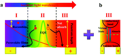 | ||
| Fig. 1 Mechanism illustration of (a) highly narrowband photodetectors and (b) TPA photodetectors based on all inorganic halide perovskites. | ||
Interestingly, perovskites have been frequently reported to possess a high TPA cross-section and related photoluminescence (PL),30–32 indicating their photoresponse possibility in another waveband, near-infrared.15,33,34 If the carriers excited through the TPA process can be collected by electrodes (Fig. 1b), secret keys can be sent with related light while other photodetectors show no response in this region, especially those with a narrowband detection ability. Additionally, the TPA process only takes place efficiently in a specific wavelength region. The excitation efficiency for shorter wavelength light is relatively low while three-photon absorption would occur for longer wavelength light, which also possesses lower efficiency. Therefore, the photoresponse through the TPA process will also exhibit a narrowband phenomenon.
Basic performance of narrowband photodetectors
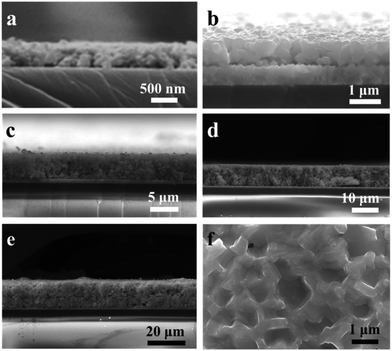
The schematic demonstration of the device configuration and the microscopy image of interdigital electrodes are shown in Fig. S4.† Here, perovskite CsPbBr3 was chosen as an example and a centrifugation strategy was applied for the perovskite film fabrication.35 To find out the critical film thickness for highly narrowband photodetectors, devices with different film thicknesses from 0.5 to 16 microns were fabricated and treated according to our previous reports (Fig. 2).17 The cross-sectional SEM images indicate that the as-fabricated films show a uniform thickness (Fig. 2f). The EQE values of the devices with different film thicknesses as a function of wavelength were measured as shown in Fig. 3. With the increase of film thickness, the EQE decreases monotonously while a peak emerges, and finally, only one sharp peak was left in the EQE spectrum (Fig. 3). The curve structure is almost like that of the PL spectrum. It implies that 16 μm is the appropriate thickness for narrowband photodetectors. The decreased EQE can be assigned to the carrier recombination resulting from the long diffusion distance. However, one should note that this value (Fig. 3, ∼15%) is higher than those reported in most of the previous studies with complicated fabrication procedures.5,6 The difference in these EQE spectra is the small redshift of the peak wavelength, which can be assigned to the following two reasons. Firstly, as shown in Fig. 1, higher energy photons have a shorter penetration depth. When the film thickness is increased, higher energy photons cannot pass through the film, resulting in ultra-low response. As a result, photons with energy close to the band edge (lower energy) will contribute more to the response, which looks like redshift behavior. Such a phenomenon has also been reported in a previous study.5 Secondly, the size increase also contributes to the small redshift. The thinnest film was fabricated without any treatment. However, when preparing films with a large thickness, several deposition steps were conducted and solution treatment was carried out before every deposition of the next layer. As reported in our previous report, the solution treatment will result in a size increase.17 This is also confirmed from the SEM images in Fig. 2a (about 100 nm) and Fig. 2f (about 500 nm) and the absorption spectra of the thinnest and the thickest films (Fig. S5†).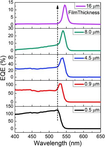 | ||
| Fig. 3 EQE of the devices with different film thicknesses as a function of wavelength under a bias of 9 V. | ||
The perovskite film shows a monoclinic phase structure (PDF#18-0346) with high crystallinity (Fig. S6†), which can also undergo anion exchange reactions as shown in Fig. S6a.†36 Similar to NCs,19,37 the color of the films varied from white to black, exhibiting PL ranging from violet to red (Fig. S6a and b†). From CsPbCl3 to CsPb(Br/I)3, the diffraction peaks shift to small angles due to the increased crystal lattice but all the films keep their crystal structure the same as CsPbBr3 (Fig. S6c†). The SEM and EDS results of the as-prepared CsPb(Br/I)3 film can be seen in Fig. S6.† As a result, highly narrowband photodetectors with a spectrally selective detection ability from violet to red are achieved based on the above mechanism (Fig. S6d†).
Two-photon-excitation photodetective behaviours
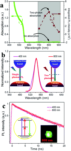
Normally, semiconductors show continuum absorption in the wavelength region above the bandgap (Fig. 4a), therefore, it is meaningless to send a secret key with light in that region for security because most of the photodetectors can perform identically. However, no absorption takes place beyond that region and the above photodetectors can only respond to a narrowband. The photoresponse from the special absorption process is necessary to achieve the functions mentioned above. Under the excitation of femtosecond laser light with the photo energy larger than the bandgap, bright green luminescence was observed for the narrowband photodetectors (Fig. 4c inset). Fig. 4a shows the PL intensity at different excitation wavelengths from 700 to 900 nm; under the excitation of 800 nm laser light, the CsPbBr3 film shows the highest PL intensity.The PL spectra excited at optical wavelengths of 400 and 800 nm, which correspond to one- and two-photon excitation processes, respectively, are shown in Fig. 5b. It is found that the emission peaks from single- and two-photon excitation processes show a negligible shift. The TPA process was also confirmed by the quadratic relationship between the integrated PL intensity and the excitation density shown in Fig. S1.† To gain more insight into the photocarriers, the dynamics based on one- and two-photon excitation are probed. The PL decay curves in Fig. 4c indicate that the decay traces for all of the two excitation mechanisms are almost the same. Then it can be concluded that the photocarriers excited by either one-photon or two-photon absorption through virtual states will relax to the same lowest excited state as illustrated in Fig. 5c inset. Therefore, it is possible to use the TPA processed photocarriers for detection.
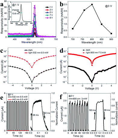
The narrowband and TPA photodetector performances are shown in Fig. 5. For a narrowband photodetector, the responsivity increases monotonically with the increase of bias, reaching a responsivity of more than 50 mA W−1, which is higher than most of the previous reports (Fig. 5a).38,39 With the increase of bias, the EQE increased monotonically and the highly narrowband behavior was maintained even under a high bias of 9 V (Fig. S2†), indicating the appropriate carrier drifting length and thickness of perovskites. It is worth noting that the FWHM is as narrow as 13.6 nm under a bias of 1 V, which is the narrowest value compared to state-of-the-art narrowband photodetectors (Fig. 5a inset).5,6,38–41 Such a highly narrow FWHM ensures the intensively selective detection of the main information so that the influence of other irradiation and background is suppressed completely.
To investigate the TPA photodetector performances, responsivity at different excitation wavelengths is determined and shown in Fig. 5b. Similar to the PL intensity, the device under the excitation at 800 nm exhibits the highest responsivity. Due to the relatively low absorption coefficient, the TPA related responsivity is smaller than that of narrowband photodetectors, but is enough for data transmission. In addition, as discussed above, due to the limitation of the excitation wavelength for the TPA process, the photodetectors also exhibit a narrowband behavior though the FWHM is relatively larger than that of the above visible light narrowband photodetectors. However, the value is smaller than those of most of the conventional narrowband devices.
Both the photocurrents for two kinds of functions under the illumination of 532 and 800 nm laser (TPA process) light are more than two orders of magnitude higher than the dark currents (Fig. 5c and d), which increase drastically under illumination with the increase of applied bias, demonstrating a nonlinear I–V behavior and a Schottky contact between the perovskite film and gold electrode. The photocurrent density can reach up to 1.5 × 10⁻³ A cm−2 even under weak illumination (0.5 mW), manifesting the merits of the films with high crystallinity, compactness, and conductivity. The current density is comparable to those reported in several similar studies and proved to be one of the best results.40,42 To gain insights into the photoswitching characteristics for communication, I–t curves with and without illumination under a bias of 3 V were obtained for both the functions (Fig. 5e and f). The laser light was controlled by using a shutter with a preset program. Upon the opening of the shutter, the current rises sharply and it decays to low values when the shutter is closed. The extracted rise times are 26 and 193 ms and the decay times are 62 and 99 ms for the two functions, respectively. The spectrally selective detection was also confirmed by the negligible response to 442 nm laser light (Fig. 5e).
Security communication based on dual-mode narrowband photodetectors
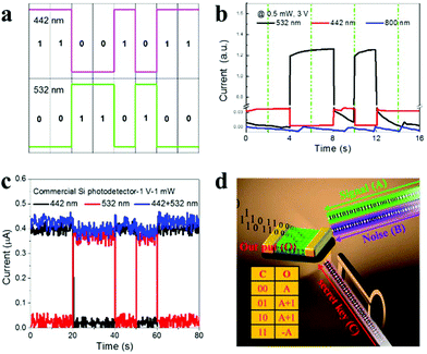
According to the above results, we have assembled visible and near-infrared dual-mode narrowband photodetection characteristics within a single device successfully and no related results have been reported until now to the best of our knowledge. Consequently, we proposed that we can send information signals and secret keys with the corresponding light while a noise signal is also sent out simultaneously.5,6,42 For example, two totally opposite signals are sent via 532 (signal A, main information) and 442 (signal B, noise signals) nm laser lights with the same intensity (Fig. 6a). Theoretically, for the as-fabricated special photodetectors, only the main information (A) can be detected while for other commercial photodetectors, both information and noise signals are detected. Such chaotic data for the current commercial photodetectors are useless. Additionally, owing to the near-infrared wavelength detection ability of the photodetectors as demonstrated above, we can send secret keys with this wavelength region for more reliable security communication.Fig. 6b shows the response behaviors of the photodetector to different wavelengths, 442, 532, and 800 nm (here 800 nm is the common light from a Xenon lamp), respectively. It should be noted that in Fig. 5d, the 800 nm light is from a femtosecond laser, which is strong enough to cause the TPA process and a large photoresponse can be seen. However, the 800 nm light from a Xenon lamp is too weak to cause the TPA process. In other words, no absorption takes place at this wavelength for our perovskite semiconductor and then no response can be observed. In Fig. 6b, 800 nm light acts as a noise signal to confirm the selective detection. Obviously, the photodetector only responds to 532 nm light and the waveform is the same as the light source shown in Fig. 6a, implying the complete acquisition of the main information. Meanwhile, no responses are observed to common 442 and 800 nm laser light. The curves of two light sources sending signals simultaneously are shown in Fig. S8.† The illumination of noise signals (442 nm and 800 nm) does not influence the I–V curves and photocurrents are more than two orders of magnitude higher than the dark currents. Apparently, the as-fabricated photodetector will not be affected by other irradiation and the environmental background. In contrast, when a commercial Si PIN photodetector was taken as the control, both the lights induce current variation (Fig. 6c). To be specific, when the Si photodetector receives the light separately, the waveform is identical to the light source in Fig. 6a and the photocurrent is similar. However, when the two light sources send signals simultaneously, the photocurrent is almost unchanged. In this case, the Si photodetector cannot distinguish the received information totally. Namely, by using such perovskite narrowband photodetectors, this is an efficient method for encryption communication. We choose a 442 nm laser source instead of a much smaller wavelength laser source due to the following reason. Photons pumped by the 442 nm laser have a smaller energy and longer penetration depth. That is, the narrowband detector will not respond to 400 nm light, for example, if it does not respond to 442 nm light. It is more convincing to choose a 442 nm laser as a noise source for selective detection for the narrowband detector.
In our manuscript, double encryptions are carried out, in which signals and secret keys are sent separately. It is clear that the narrowband photodetector could receive information accurately and is free from the influence of common 442 and 800 nm light, which is superior in encryption compared with commercial Si detectors. For further encryption, the final output information (O) will be determined according to the secret key (signal C) sent with near-infrared laser light as illustrated in Fig. 6d. For example, we can deal with the information signal (A) according to the following manner. If C is ‘00’ (0 means no light and 1 means under illumination), the output signal O can be A itself, if C is ‘01’ or ‘10’, O can be A + 1, and if C is ‘11’, O can be −A (inverse the data, 0 to 1 and 1 to 0). Notably, all the data processing procedures are based on the binary system. Specifically, if the information is as illustrated in Fig. 6a and we convert it to decimal data, the output signal is 52 if C is ‘00’. When C is ‘01’ or ‘10’, the output signal is 53 and when C is ‘11’, the output signal is 203. The above data processing method is just for example, we can put forward any algorithm for encryption as required. It is worth noting that the merits of such an encryption technique are not the numerical calculation, but the interesting photodetector characteristics that can encrypt with a facile strategy.
Device and performance stabilities are well-known issues for halide perovskite based applications especially for perovskites. When the device was stored under ambient conditions, no deterioration was observed after 50 days even when no protection strategies were applied (Fig. S3, S7b and S9†), indicating its high environmental stability and potential applications in the future. Besides, the ultra-long term (more than 10 hours) switching behavior was measured under continuous light illumination as shown in Fig. S9b.† Interestingly, the photocurrent increased gradually, which might be attributed to the polarization resulting from ion migration.15,43 The detailed influence of this effect on devices and its elimination will be studied in the future.
Conclusion
In summary, in this work, we report the first demonstration of the highly narrowband and TPA related detection abilities within one device fabricated with all inorganic halide perovskites through solution methods. The narrowest FWHM of 13.6 nm, spectrally tunable photodetection by anion exchange, and efficient carrier collection for TPA processes are achieved. By combining these two photoresponse behaviors in the visible and near-infrared wavelength regions together within one device, we introduce an encryption technique for security communication, that is sending information and noise signals with different laser light simultaneously and the photodetectors only receive the workable information. In contrast, the commercial photodetectors respond to both lights, losing the main information completely. A secret key was also sent after the transmission of the information signal, making some data conversion as preset. Such narrowband and TPA detection abilities endow the photodetectors with great potential in future security communication and also provide new opportunities and platforms for encryption techniques.Experimental section
Fabrication of the perovskite photodetectors
The interdigitated electrodes were purchased from Nanjing MKNANO Tech. Co., Ltd and used directly with a finger width of 20 μm. The thick and compact CsPbBr3 films were deposited with a centrifugal casting method according to our previous reports.16,17 Specifically, Au/Cr/SiO2/Si integrated electrodes were soaked in CsPbBr3 NC/toluene dispersion and centrifuged for 3 min, which were dried and annealed at 70 °C for 10 min. Then, the films were treated with a mixed solution of toluene (4 μL) and ethanol (10 μL) three times, and after which a 250 °C treatment in air was carried out for 0.5 h. The film thickness was controlled by solution concentration and repeated depositions. Namely, for thinner films (0.5 and 0.9 μm), diluted solutions were used. For films thicker than 4.5 μm, after the first deposition of the CsPbBr3 layer, another or several depositions were conducted. One should note that before the deposition of the latter perovskite layer, the above solution film treatment is necessary to ensure compact films. The anion exchange reactions were conducted according to ref. 44.Measurements of the perovskite photodetectors
The single-photon related EQE and responsivity were characterized with a Zolix DSR-101-UV system equipped with a Si photodetector as the reference while a Ti:sapphire femtosecond laser (Spitfire Ace, Spectra-Physics, 1 kHz, 120 fs) was applied for two-photon related performances. The on/off cycling performances and response speed were measured with a trigger equipped with an oscilloscope. All the current results were obtained with a Keithley 6487.Material characterization
The absorption spectra were obtained with a Shimadzu 3600 UV/Vis spectrophotometer. Photoluminescence spectra were obtained using a Princeton SP2000. XRD patterns and SEM images were recorded on a Bruker D8 Advance and a FEI Quanta 250F field emission electron microscope, respectively. The PL lifetime was determined and analyzed by using an Optronics streak camera system with an optimized temporal resolution of ≈50 ps.Conflicts of interest
There are no conflicts to declare.Acknowledgements
This work was financially supported by the National Key Basic Research Program of China (2014CB931702), NSFC (51572128, 21403109), NSFC-RGC (5151101197), the National Key Research and Development Program of China (2016YFB0401701), the Fundamental Research Funds for the Central Universities (No. 30915012205, 30916015106), the Natural Science Foundation of Jiangsu Province (BK20140769), and PAPD of Jiangsu Higher Education Institutions.Notes and references
- L. Gu, M. M. Tavakoli, D. Zhang, Q. Zhang, A. Waleed, Y. Xiao, K.-H. Tsui, Y. Lin, L. Liao, J. Wang and Z. Fan, Adv. Mater., 2016, 28, 9713–9721 CrossRef CAS PubMed.
- I. Dursun, C. Shen, M. R. Parida, J. Pan, S. P. Sarmah, D. Priante, N. Alyami, J. Liu, M. I. Saidaminov, M. S. Alias, A. L. Abdelhady, T. K. Ng, O. F. Mohammed, B. S. Ooi and O. M. Bakr, ACS Photonics, 2016, 3, 1150–1156 CrossRef CAS.
- X. Hu, X. Zhang, L. Liang, J. Bao, S. Li, W. Yang and Y. Xie, Adv. Funct. Mater., 2014, 24, 7373–7380 CrossRef CAS.
- L. Shen, Y. Fang, D. Wang, Y. Bai, Y. Deng, M. Wang, Y. Lu and J. Huang, Adv. Mater., 2016, 28, 10794–10800 CrossRef CAS PubMed.
- Y. Fang, Q. Dong, Y. Shao, Y. Yuan and J. Huang, Nat. Photonics, 2015, 9, 679–686 CrossRef CAS.
- Q. Lin, A. Armin, P. L. Burn and P. Meredith, Nat. Photonics, 2015, 9, 687–694 CrossRef CAS.
- M. He, Y. Chen, H. Liu, J. Wang, X. Fang and Z. Liang, Chem. Commun., 2015, 51, 9659–9661 RSC.
- H.-R. Xia, J. Li, W.-T. Sun and L.-M. Peng, Chem. Commun., 2014, 50, 13695–13697 RSC.
- Y. Fang and J. Huang, Adv. Mater., 2015, 27, 2804–2810 CrossRef CAS PubMed.
- H. Wei, Y. Fang, P. Mulligan, W. Chuirazzi, H.-H. Fang, C. Wang, B. R. Ecker, Y. Gao, M. A. Loi, L. Cao and J. Huang, Nat. Photonics, 2016, 10, 333–339 CrossRef CAS.
- G. Konstantatos and E. H. Sargent, Appl. Phys. Lett., 2007, 91, 173505 CrossRef.
- J. Liu, J. Michel, W. Giziewicz, D. Pan, K. Wada, D. D. Cannon, S. Jongthammanurak, D. T. Danielson, L. C. Kimerling, J. Chen, F. Ö. Ilday, F. X. Kärtner and J. Yasaitis, Appl. Phys. Lett., 2005, 87, 103501 CrossRef.
- A. Srinivasan, S. Murtaza, J. C. Campbell and B. G. Streetman, Appl. Phys. Lett., 1995, 66, 535–537 CrossRef CAS.
- A. C. Goldberg, S. W. Kennerly, J. W. Little, T. A. Shafer, C. L. Mears, H. F. Schaake, M. Winn, M. Taylor and P. N. Uppal, Opt. Eng., 2003, 42, 30–46 CrossRef CAS.
- Y. Wang, X. Li, X. Zhao, L. Xiao, H. Zeng and H. Sun, Nano Lett., 2016, 16, 448–453 CrossRef CAS PubMed.
- X. Li, Y. Wu, S. Zhang, B. Cai, Y. Gu, J. Song and H. Zeng, Adv. Funct. Mater., 2016, 26, 2435–2445 CrossRef CAS.
- X. Li, D. Yu, F. Cao, Y. Gu, Y. Wei, Y. Wu, J. Song and H. Zeng, Adv. Funct. Mater., 2016, 26, 5903–5912 CrossRef CAS.
- M. Kulbak, D. Cahen and G. Hodes, J. Phys. Chem. Lett., 2015, 6, 2452–2456 CrossRef CAS PubMed.
- Y. Wang, X. Li, J. Song, L. Xiao, H. Zeng and H. Sun, Adv. Mater., 2015, 27, 7101–7108 CrossRef CAS PubMed.
- D. M. Lyons, A. Armin, M. Stolterfoht, R. C. R. Nagiri, R. D. Jansen-van Vuuren, B. N. Pal, P. L. Burn, S.-C. Lo and P. Meredith, Org. Electron., 2014, 15, 2903–2911 CrossRef CAS.
- S. Nishiwaki, T. Nakamura, M. Hiramoto, T. Fujii and M.-a. Suzuki, Nat. Photonics, 2013, 7, 248–254 CrossRef CAS.
- A. Sobhani, M. W. Knight, Y. Wang, B. Zheng, N. S. King, L. V. Brown, Z. Fang, P. Nordlander and N. J. Halas, Nat. Commun., 2013, 4, 1643 CrossRef PubMed.
- M. G. Han, K.-B. Park, X. Bulliard, G. H. Lee, S. Yun, D.-S. Leem, C.-J. Heo, T. Yagi, R. Sakurai, T. Ro, S.-J. Lim, S. Sul, K. Na, J. Ahn, Y. W. Jin and S. Lee, ACS Appl. Mater. Interfaces, 2016, 8, 26143–26151 CAS.
- M. I. Saidaminov, M. A. Haque, M. Savoie, A. L. Abdelhady, N. Cho, I. Dursun, U. Buttner, E. Alarousu, T. Wu and O. M. Bakr, Adv. Mater., 2016, 28, 8144–8149 CrossRef CAS PubMed.
- Y. Wang, X. Li, S. Sreejith, F. Cao, Z. Wang, M. C. Stuparu, H. Zeng and H. Sun, Adv. Mater., 2016, 28, 10637–10643 CrossRef CAS PubMed.
- J. Song, J. Li, X. Li, L. Xu, Y. Dong and H. Zeng, Adv. Mater., 2015, 27, 7162–7167 CrossRef CAS PubMed.
- J. De Roo, M. Ibáñez, P. Geiregat, G. Nedelcu, W. Walravens, J. Maes, J. C. Martins, I. Van Driessche, M. V. Kovalenko and Z. Hens, ACS Nano, 2016, 10, 2071–2081 CrossRef CAS PubMed.
- G. R. Yettapu, D. Talukdar, S. Sarkar, A. Swarnkar, A. Nag, P. Ghosh and P. Mandal, Nano Lett., 2016, 16, 4838–4848 CrossRef CAS PubMed.
- C. C. Stoumpos, C. D. Malliakas, J. A. Peters, Z. Liu, M. Sebastian, J. Im, T. C. Chasapis, A. C. Wibowo, D. Y. Chung, A. J. Freeman, B. W. Wessels and M. G. Kanatzidis, Cryst. Growth Des., 2013, 13, 2722–2727 CAS.
- K. Wei, Z. Xu, R. Chen, X. Zheng, X. Cheng and T. Jiang, Opt. Lett., 2016, 41, 3821–3824 CrossRef CAS PubMed.
- W. G. Lu, C. Chen, D. Han, L. Yao, J. Han, H. Zhong and Y. Wang, Adv. Opt. Mater., 2016, 4, 1732–1737 CrossRef CAS.
- Y. Xu, Q. Chen, C. Zhang, R. Wang, H. Wu, X. Zhang, G. Xing, W. W. Yu, X. Wang, Y. Zhang and M. Xiao, J. Am. Chem. Soc., 2016, 138, 3761–3768 CrossRef CAS PubMed.
- J. Pan, S. P. Sarmah, B. Murali, I. Dursun, W. Peng, M. R. Parida, J. Liu, L. Sinatra, N. Alyami, C. Zhao, E. Alarousu, T. K. Ng, B. S. Ooi, O. M. Bakr and O. F. Mohammed, J. Phys. Chem. Lett., 2015, 6, 5027–5033 CrossRef CAS PubMed.
- G. Walters, B. R. Sutherland, S. Hoogland, D. Shi, R. Comin, D. P. Sellan, O. M. Bakr and E. H. Sargent, ACS Nano, 2015, 9, 9340–9346 CrossRef CAS PubMed.
- M. Chen, H. Cölfen and S. Polarz, ACS Nano, 2015, 9, 6944–6950 CrossRef CAS PubMed.
- Q. A. Akkerman, V. D'Innocenzo, S. Accornero, A. Scarpellini, A. Petrozza, M. Prato and L. Manna, J. Am. Chem. Soc., 2015, 137, 10276–10281 CrossRef CAS PubMed.
- L. Protesescu, S. Yakunin, M. I. Bodnarchuk, F. Krieg, R. Caputo, C. H. Hendon, R. X. Yang, A. Walsh and M. V. Kovalenko, Nano Lett., 2015, 15, 3692–3696 CrossRef CAS PubMed.
- Q. Lin, A. Armin, P. L. Burn and P. Meredith, Laser Photonics Rev., 2016, 10, 1047–1053 CrossRef CAS.
- W. Li, D. Li, G. Dong, L. Duan, J. Sun, D. Zhang and L. Wang, Laser Photonics Rev., 2016, 10, 473–480 CrossRef CAS.
- A. Armin, R. D. Jansen-van Vuuren, N. Kopidakis, P. L. Burn and P. Meredith, Nat. Commun., 2015, 6, 6343 CrossRef CAS PubMed.
- L. Shen, Y. Fang, H. Wei, Y. Yuan and J. Huang, Adv. Mater., 2016, 28, 2043–2048 CrossRef CAS PubMed.
- L. Shen, Y. Zhang, Y. Bai, X. Zheng, Q. Wang and J. Huang, Nanoscale, 2016, 8, 12990–12997 RSC.
- R. Gottesman, E. Haltzi, L. Gouda, S. Tirosh, Y. Bouhadana, A. Zaban, E. Mosconi and F. De Angelis, J. Phys. Chem. Lett., 2014, 5, 2662–2669 CrossRef CAS PubMed.
- G. Nedelcu, L. Protesescu, S. Yakunin, M. I. Bodnarchuk, M. J. Grotevent and M. V. Kovalenko, Nano Lett., 2015, 15, 5635–5640 CrossRef CAS PubMed.
Footnote |
| † Electronic supplementary information (ESI) available. See DOI: 10.1039/c7nr06193e |
| This journal is © The Royal Society of Chemistry 2018 |

