
 Open Access Article
 This Open Access Article is licensed under a Creative Commons Attribution-Non Commercial 3.0 Unported Licence
Experimental and computational insights into CuS–Mg composites for high-performance p-type transparent conducting materials†
Stener
Lie
 a,
Qingde
Sun
a,
Pritish
Mishra
ab,
Patrick Wen Feng
Li
b,
Anupam
Sadhu
a,
Teddy
Salim
b,
Shuzhou
Li
b,
Geoffroy
Hautier
c and
Lydia Helena
Wong
*b
a,
Qingde
Sun
a,
Pritish
Mishra
ab,
Patrick Wen Feng
Li
b,
Anupam
Sadhu
a,
Teddy
Salim
b,
Shuzhou
Li
b,
Geoffroy
Hautier
c and
Lydia Helena
Wong
*b
aEnergy Research Institute at NTU, Nanyang Technological University, 637141, Singapore
bSchool of Materials Science & Engineering, Nanyang Technological University, 50 Nanyang Ave, 639798, Singapore. E-mail: lydiawong@ntu.edu.sg
cThayer School of Engineering, Dartmouth College, Dartmouth College, Hanover, NH 03755, USA
First published on 17th February 2025
Abstract
Achieving fully transparent electronic devices requires improving p-type transparent conducting materials (TCMs) to match their n-type counterparts. This study explores novel p-type TCMs using high-throughput screening via an automatic spray pyrolysis system. The performance of conducting wide bandgap chalcogenide based on CuS can be improved by incorporating various cations, with Mg emerging as the most promising candidate. The optimized CuS–Mg films exhibited superior transparency and conductivity, comparable to state-of-the-art p-type TCMs. Density functional theory (DFT) calculations linked the inverse correlation between transparency and conductivity to changes in Cu 3d and S 3p orbital coupling with varying Mg content. The best CuS–Mg composition demonstrated high hole concentration (5 × 1021 cm−3), low sheet resistance (266 Ω □−1), and high transparency (∼75%). The transmittance increased by ∼30% compared with pristine CuS. The successful application of a p-CuS–Mg/n-CdS heterojunction as a semi-transparent photodiode highlights its potential for smart displays and window-integrated electronics. This study demonstrates the value of combining experimental and theoretical methods for accelerated material discovery.
New conceptsThis study presents a high-throughput screening approach using an automated spray pyrolysis system to discover novel p-type transparent conducting materials (TCMs) by combining wide bandgap chalcogenides with CuS. This method not only eliminates the downtime typically associated with traditional material screening techniques but also significantly reduces fabrication time while optimizing processing parameters. By integrating experimental and computational techniques, the approach provides a deep understanding of the mechanisms governing conductivity and transparency in the materials. In contrast to conventional methods that achieve high-performing p-type TCMs through doping of wide bandgap oxides, this approach starts with a highly conductive p-type material, CuS, and enhances transparency through the incorporation of Mg, which weakens p–d coupling and induces amorphization. This process results in a CuS–Mg candidate with a figure of merit among the highest reported for p-type TCMs. This strategy not only introduces a novel mechanism to explain the observed properties but also establishes a versatile framework for accelerating material discovery and optimization across various fields. |
Introduction
Smart electronic devices rely on advanced screen technology, which has been made possible by the discovery of n-type transparent conductors. While n-type transparent conductors like indium tin oxide (ITO) are widely used,1 the unavailability of p-type transparent conductors in the market is mainly attributed to the failure of possessing both superior transparency and p-type conductivity. The lack of high-quality p-type transparent conductors limits the development of smart transparent devices that require selective contacts for efficient charge extractions. These devices include semi-transparent solar cells,2–4 electrochromic glass windows,5–7 light-emitting diodes,8,9 and sensors.10,11 The widely studied transparent conducting materials are oxides due to their wide band gap; however, these materials are typically intrinsically resistive or non-conductive. To enhance their conductivity, external doping is commonly used, as observed in the case of tin-doped indium oxide (ITO). The doping of tin can increase the carrier concentration to a range of 1018–1021 cm−3 and enhance the conductivity to the range of 103–104 S cm−1 while maintaining excellent visible light transmission of about 85–90%.12 However, achieving high-performing p-type TCMs through similar doping strategies with oxide-based materials proves to be challenging. According to the doping limits rule summarized by Zunger et al.,13,14 it is challenging to effectively achieve p-type doping due to the relatively low valence band maximum (VBM) caused by the deep level of O 2p orbitals in TCO (Transparent Conductive Oxides).15 Chemical modulation of the valence band (CMVB), as proposed by Hosono et al.,16 is an effective strategy for elevating VBM by introducing a p–d coupling effect. Among the metal cations with closed shells of d10s0, Cu is the most promising candidate for CMVB, as shown by the variously reported CuMO2 (M = Al, Ga, In, Sc, Y, Cr) delafossite structures.17 Nonetheless, the 2D dumbbell-shaped O–Cu–O of delafossite structure was not expected to exhibit high mobility and conductivity. Therefore, the utilization of materials with alternative anions possessing relatively low electronegativity, such as sulfide, presents a viable pathway towards achieving higher conductivity in p-type TCMs.CuS has emerged as a promising candidate for conducting material and has been employed in various optoelectronic devices, including solar cells and photodetectors.18–20 Also known as the covellite phase, it possesses a hexagonal structure with CuS4 tetrahedral and CuS3 triangular coordination. CuS is an intrinsically p-type material with a bandgap ranging from 1.5–2.3 eV and exhibit high conductivity (∼103 S cm−1).21 In addition, CuS is non-toxic, abundant, and cost-effective, making it an ideal material for large-scale production. However, even in its nanostructured morphology, CuS exhibits a relatively narrow band gap (∼2.4 eV),22,23 resulting in poor transparency, particularly in the visible range. Therefore, it is crucial to develop a strategy to enhance its transparency and enable it to be an efficient transparent conductor. One approach to improve the transparency of CuS is to reduce its thickness to be ultrathin. For instance, CuS nanowires have demonstrated very high transparency of up to 80%.24 However, this method presents challenges, such as the requirement for encapsulation or protection layers such as polymer layers to prevent the mechanical failure of the CuS nanowires. Moreover, the fabrication methods for ultrathin CuS are not easily scalable and reliable for industrial processes. Another strategy involves the incorporation of CuS with wide band gap binary sulfide compounds to create composite films that combine the conductivity of CuS and the higher transparency of the binary sulfide. ZnS is the most well-known compound used in combination with CuS to form (CuS)x:(ZnS)1−x composite films.22,25,26 However, as the proportion of ZnS increases, the conductivity decreases significantly, despite the improvement in transparency. Although other wide band gap chalcogenides may also serve as suitable combination options, there are currently no reported literature findings showing comparable performance.
Therefore, in this study, we employed a high-throughput screening approach utilizing an automated spray pyrolysis system (schematic of the system is shown in Fig. S1, ESI†) to explore alternative combinations of cations with CuS to fabricate conducting wide band gap chalcogenides. This method not only eliminates the downtime associated with traditional spraying techniques but also significantly reduces the fabrication time by two-thirds. The downtime reduction encompasses processes such as the hotplate's ramping up and down, sample loading, and precursor loading, streamlining the experimentation process. In selecting suitable cations, we initially considered the wide band gap binary chalcogenide compounds, such as BaS (3.8 eV),27 MgS (4.5 eV),28 SrS (4.2 eV),29 or CaS (4.4 eV).30 Additionally, we conducted screening based on cation oxidation states, prioritizing cations with an oxidation state of +2, akin to ZnS. Further refinement involved exploring cations recognized as dopants known to enhance the conductivity of certain p-type Transparent Conductive Materials (TCMs). For example, Mg is a well-known dopants in Cu2O,31 LaCuOSe,32 Cr2O3,33 and CuCrO2;34 Sr acts as dopant in La-based TCMs such as LaCuOS,35 LaCrO3;36 while Ca is also a dopant for SrCu2O2.37 Incorporating such cations into the CuS lattice was anticipated to modify the electronic structure, thereby enhancing transparency without compromising conductivity significantly. Ultimately, we selected seven cations—Ba, Cd, Mg, Mn, Sr, Ca, and Zn for our investigation. Among these, Mg emerged as a promising candidate, prompting further investigation into optimal process fabrication parameters using the high-throughput technique. Subsequently, we evaluated the potential of CuS–Mg films as a p-type TCM, employing a normal spray pyrolysis setup with precise control. To elucidate the optoelectronic changes, a combination of computational studies through DFT and characterizations such as X-ray Photoelectron Spectroscopy (XPS) and AC Hall measurements were performed. The CuS–Mg film demonstrated performance comparable to highly effective p-type TCMs reported in the literature. This comprehensive approach not only presents a novel methodology but also establishes Mg-doped CuS as a promising transparent conductor.
Results and discussions
Screening for optimized wide band gap chalcogenides
Table 1 summarizes the different types of cations used to enhance the transparency of CuS. In this screening study, we replaced 50% of Cu with the respective substituent cations in the precursor solution. The fabrication parameters were kept consistent for all the cations. The addition of Cd did not alter the band gap, as the band gap of CdS38 is comparable to that of CuS. All cations, except for Ba and Sr, led to an increase in band gap, with Mg and Zn showing the highest increase. The incorporation of all cations in CuS resulted in higher average visible transmittance (%), however for Ba, it exhibited lower transmittance at 550 nm compared to pristine CuS. The increase in transparency inadvertently led to an increase in sheet resistance, although the extent of the decrease varied among the cations. Overall, only Mn and Mg demonstrated as low resistance as Zn. To holistically assess their performance in terms of both transparency and conductivity, the figure of merit (FOM) values introduced by Haacke39 (FOMH) and Gordon40 (FOMG) are used as benchmarks. FOMG emphasizes the conductivity, whereas FOMH places more importance on transparency as key aspects of TCMs. We obtained FOMH ranging from 101 to 102 × 10−6 Ω−1 for CuS–Mg, CuS–Mn and CuS–Zn, which are comparable to those of high-performing p-type TCMs, such as LaCuOSe, La0.67Sr0.33VO3, CuCrO2, CuI.17,26,41 Meanwhile, based on FOMG, CuS–Mg and CuS–Mn outperformed CuS–Zn, but both compounds were behind CuS due to their very low resistance. Based on this analysis, it is concluded that CuS–Mg exhibited the highest FOMH and FOMG values among the cation-modified samples. Furthermore, Mg is also an abundant element and can serve as a dopant to improve the conductivity of certain p-type materials, such as Cr2O3,42 LaCuOSe,43 Ga2O3,44 CuCrO2.45| Band gap (eV) | Average Rsh (Ω □−1) | Average visible transmittance (AVT) (%) | Transmittance at 550 nm (%) | FOMH (T10/Rsh) (× 10−6 Ω−1) | FOMG 1/(Rsh·ln![[thin space (1/6-em)]](https://www.rsc.org/images/entities/char_2009.gif) T) (× 10−6 Ω−1) T) (× 10−6 Ω−1) |
|
|---|---|---|---|---|---|---|
| CuS | 2.54 | 90.18 | 32.08 | 42.13 | 0.13 | 9751.97 |
| CuS–Ba | 2.37 | 2295.20 | 34.42 | 37.65 | 0.01 | 408.51 |
| CuS–Cd | 2.54 | 9552.5 | 48.26 | 54.08 | 0.07 | 143.69 |
| CuS–Mg | 2.87 | 205.45 | 56.38 | 63.03 | 15.79 | 8492.83 |
| CuS–Zn | 2.91 | 476.99 | 56.97 | 61.55 | 7.55 | 3726.44 |
| CuS–Mn | 2.75 | 187.08 | 53.17 | 63.22 | 9.65 | 8461.22 |
| CuS–Sr | 2.52 | 5507.50 | 45.74 | 52.37 | 0.07 | 232.12 |
| CuS–Ca | 2.57 | 5.00 × 10⁻⁸ | 57.54 | 67.70 | 7.95 × 10⁻⁶ | 3.62 × 10⁻³ |
High throughput optimization of fabrication parameter
To find the most optimized solution molarity and Mg/(Mg + Cu) precursor ratio a high throughput fabrication and characterization were conducted. The samples were fabricated with Mg/(Mg + Cu) ratio from 0 to 0.6, while the molarity was varied from 2.5 to 12.5 mM. The sheet resistance and transmittance of the samples were measured and their respective FOM values were plotted in a 3D Map, as shown in Fig. 1 Darker green colors indicate better properties as TCMs, such as higher transparency and lower sheet resistance, while darker red regions indicate otherwise. In CuS–Mg thin films, an increase in Mg content and a reduction in molarity causes both transmittance and sheet resistance to increase. Notably, a sudden and significant increase in resistance is observed at an Mg content of approximately 0.4 to 0.5, as well as at molarities lower than 4 mM, even for small amounts of Mg. The molarity affects the thickness and film quality. At low molarity (2.5 mM), the thickness is approximately 100 nm, while at higher molarity (12.5 mM), the thickness can increase by 3-fold to around 300 nm (see Fig. S3, ESI†). Fig. 1(c) shows that the optimal FOMH is achieved at around 5 mM molarity and Mg/(Mg + Cu) = 0.4 while for FOMG (Fig. 1(d)) the optimal position is shown by pure CuS at a higher concentration. Interestingly, at the optimal FOMH position, the dark green region also prevails in the FOMG contour map. Therefore, the focus of this study will be on this region. | ||
| Fig. 1 Contour map of (a) average visible transmittance (AVT) (%), (b) average sheet resistance (Rs) (Ω □−1), (c) FOMH (× 10−6 Ω−1) and (d) FOMG (× 10−6 Ω−1) with respect to Mg/(Mg + Cu) and molarity variation. | ||
Evolution of CuS properties upon Mg incorporation
To further understand the effect Mg incorporation on the properties of CuS, a series of samples ranging from pure CuS, Mg-doped CuS to pure MgS were fabricated using the optimal concentration of 5 mM, but with a more precise spray fabrication method. In this series, all samples were given the same amount of heat exposure, including the time for the samples on the hotplate pre- and post-spraying pyrolysis. Fig. 2(a) shows the photograph of CuS with different amounts of Mg (Mg/(Mg + Cu) = 0, 0.2, 0.4, 0.5, 0.6, 0.8, and 1). The effect of Mg on the transparency of the films is significant. The samples have different colors, from yellowish green to transparent, as the Mg amount increases. Quantitatively, the transparency of these films increases by 10–20% with every 20% increase in Mg content, which corresponds to the increase in band gap, as shown in Table S1 and Fig. S4 (ESI†). The data and trend are consistent throughout three different batches of sample as shown through the statistical value in Table S1 (ESI†). On the other hand, the conductivity, as measured by the average sheet resistance, decreases significantly after reaching a Mg content of 0.4. Pure CuS crystallizes in the covellite phase with a hexagonal P63/mmc space group. Upon adding Mg into CuS, we observed a gradual reduction of the CuS peak, as depicted in Fig. 2(b), indicating that the film contains less CuS and becomes less crystalline This reduction becomes significant when the Mg content (x) exceeds 0.4. Across different solution molarity, similar patterns are observed, as depicted in Fig. S5 (ESI†). The reduction in the CuS peak, coupled with the appearance of an amorphous broad hump around 22°, is seen as the Mg content increases. Additionally, a Cu2S peak emerges around 15.9°, becoming more pronounced at higher solution concentrations (≥7.5 mM). The reduction in CuS peak might be due to both the reduction in Cu content as Mg increases and the decrease in crystallinity; the latter suggests that Mg destabilizes the CuS lattice, leading to the formation of an amorphous phase rather than substituting Cu in the CuS structure. In addition, the plan-view SEM and AFM images of the samples (see Fig. S6 and S7, ESI†) show the decreasing grains size of the film with increasing amount of Mg. The root-mean-square (RMS) roughness of the film decreases from around 25 nm for CuS to 2 nm for Mg–S which suggests the decrease in crystallinity and amorphous phase formation. This finding is further confirmed by transmission electron microscopy (TEM) analysis of the CuS–Mg 0.4 (Fig. S8, ESI†), which reveals a lack of long-range structural order and a TEM diffraction pattern indicating reduced crystallinity. Amorphous materials are also viable options for transparent conducting materials (TCMs) alongside crystalline materials. Utilizing amorphous materials in TCMs presents numerous advantages. They exhibit fewer inherent defects due to the absence of periodicity found in crystalline materials, resulting in smoother surfaces and interfaces.46 Moreover, they generally require lower processing temperatures, making them conducive to cost-effective large-scale production. High-performing amorphous TCMs, such as n-type a-IGZO (In–Ga–Zn–O), have been used commercially as thin film transistors (TFT) for liquid crystal displays and large organic light-emitting diode panels.47 For the p-type counterpart, only a few materials have been studied. Cu–Sn–I has emerged as a candidate, but its conductivity is lacking due to low carrier concentration (<1018 cm−3).48,49 The extra Sn cations introduced into the CuI thin film were found to inhibit the crystallization process, leading to the formation of amorphous p-type TCMs. His observation suggests that Mg in CuS might serve a similar role as Sn in CuI, potentially offering another candidate for high-performing amorphous p-type TCMs.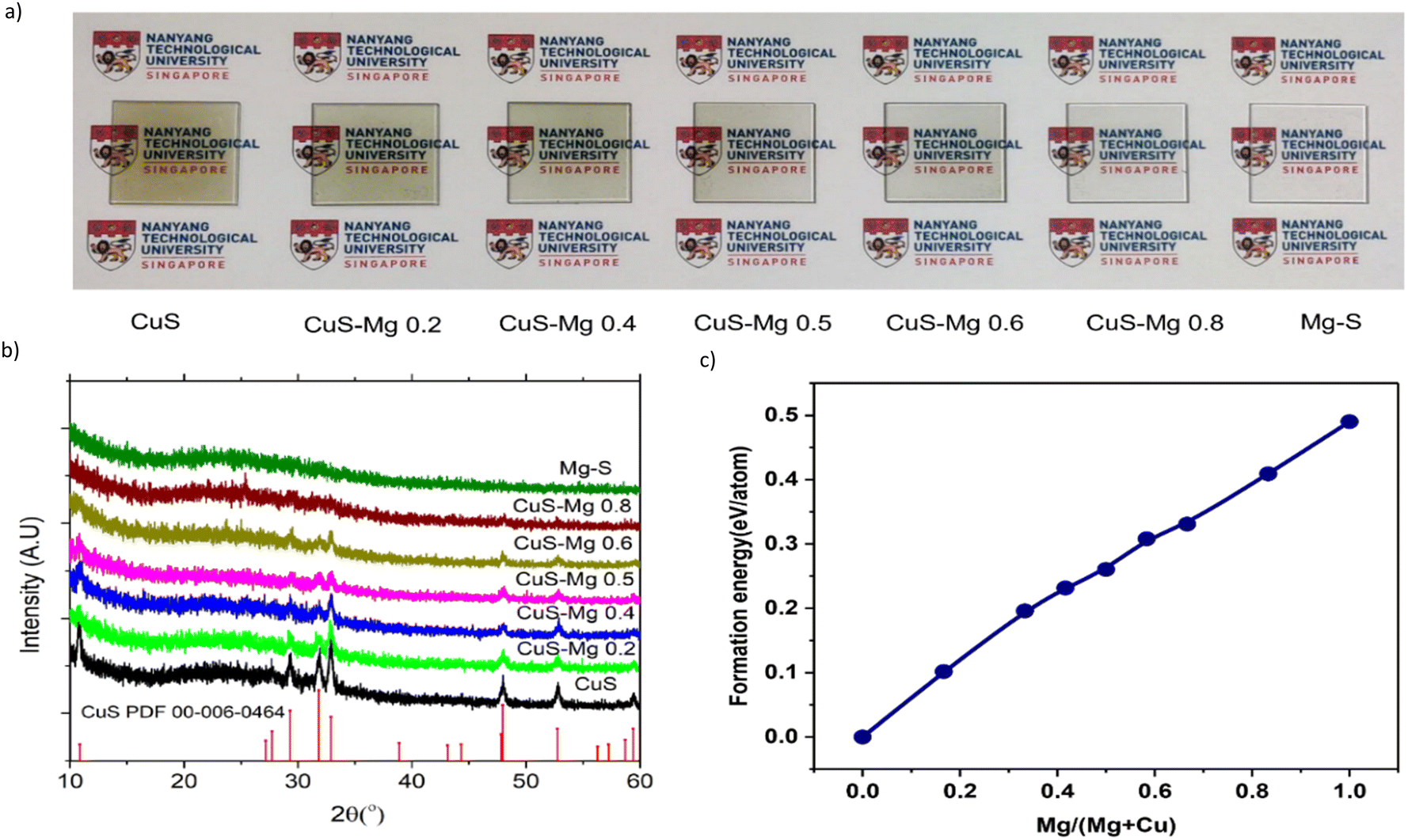 | ||
| Fig. 2 (a) Photograph of Mg-modified CuS films with varying amounts of Mg, ranging from pure CuS (leftmost) to pure MgS (rightmost). (b) X-ray diffraction spectra of CuS–Mg films with varying Mg concentrations, from pure CuS (black) to pure Mg–S (dark green). (c) Formation energy of Cu1−xMgxS (0 < x < 1) starting from pure CuS in covellite. | ||
The reduction of crystalline CuS can also be explained through DFT calculations, which show an increase in the formation energy of Cu1−xMgxS as the Mg content increases (Fig. 2(c)) in the covellite phase. The calculations reveal that at high Mg content, the covellite phase is far from the ground state, indicating its instability. The incorporated Mg did not form crystalline phase which might be due to the instability of MgS upon exposure to moisture as the fabrication method in this study was performed in air.50
To further verify the effect of Mg incorporation onto the phase formation, X-ray photoelectron spectroscopy (XPS) measurements were conducted on CuS and CuS–Mg at Mg/(Mg + Cu) = 0.4 where transformation to amorphous phase starts to occur. The XPS results provide further insights into the chemical states of each element (tabulated at Table S2, ESI†). The wide spectrum (see Fig. S9a, ESI†) of CuS is dominated by Cu and S signals, along with a small amount of C, N and O. These are possibly due to organic contamination. In contrast, CuS–Mg shows significant Mg, O, and Cl signals, suggesting the possible deposition of unreacted metal chloride precursors or formation of oxides. To further analyze this, the XPS spectra of the main elements are fitted and evaluated. Fig. 3 shows that both samples exhibit similar Cu 2p spectra, which can be deconvoluted into two sets of Cu+ peaks corresponding to the covellite (CuS) and chalcocite (Cu2S) phases.51,52 In addition, the absence of satellite features in both Cu 2p spectra suggests the lack of Cu2+ compounds, which has been previously reported for covellite CuS.52 Furthermore, the S 2p spectra in Fig. 3 also verify the presence of S22− (CuS) and S2− (Cu2S) species alongside organic thiol compound from residual thiourea. In fact, the peak fitting of Cu 2p and S 2p spectra reveals that more Cu2S phase could be detected in the Mg-modified CuS, indicating the influence of Mg in destabilizing the formation of CuS. This result suggests that Mg affects the formation of CuS by inducing amorphization and indirectly promoting more Cu2S formation in the system, as also observed in the XRD analysis. The additional peaks at 168.8 eV in the S 2p spectrum of CuS–Mg can be ascribed to the sulfonated (–SO3H) group. Fig. S9 (ESI†) presents the Mg 2p and Cl 2p spectra of CuS–Mg. The main peak Mg 2p around 50.7 eV is likely to be attributed to the MgCl2 or MgO, while the minor peak at 49.8 eV can be assigned to metallic Mg.53,54 As for Cl 2p, the peaks around 199 eV match with metal chloride.55
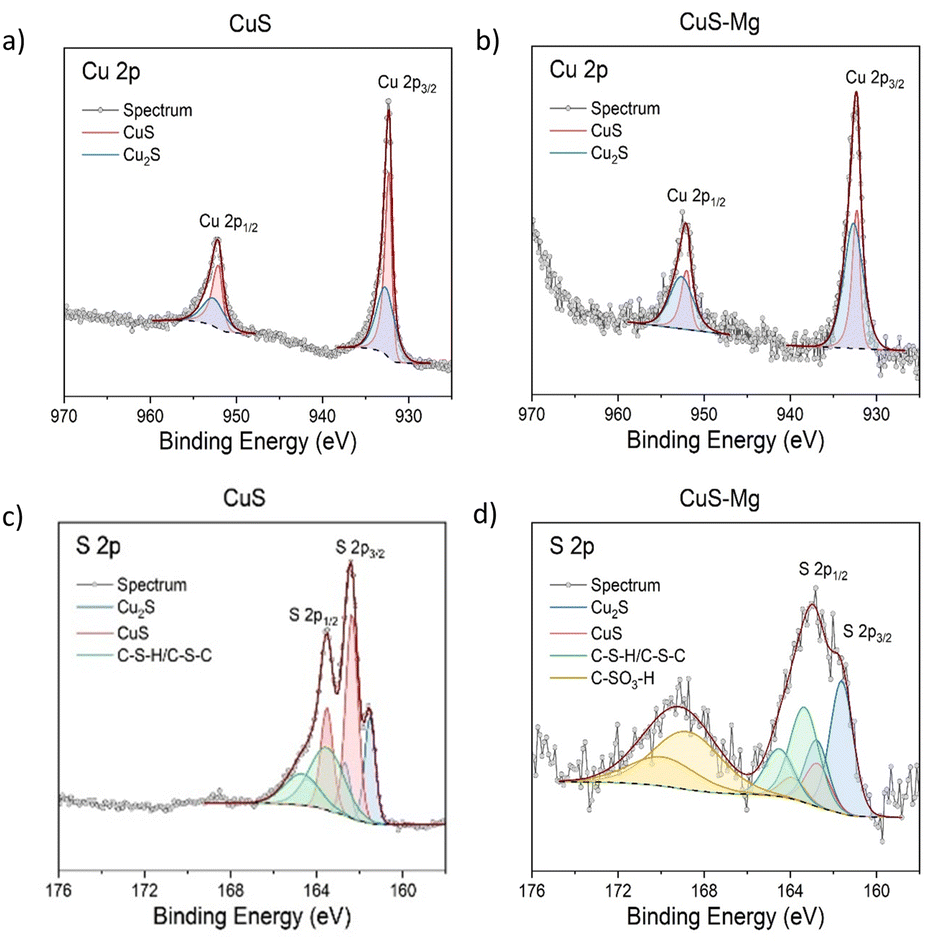 | ||
| Fig. 3 XPS spectra of Cu 2p and S 2p for (a and c) CuS and (b and d) CuS–Mg. | ||
In addition, the observed XPS also indicate the elemental composition of the film as calculated in Table S3 (ESI†). The chemical composition was quantitatively determined from the background-subtracted peak area for the core levels of interest and the corresponding relative sensitivity factor (RSF). The XPS results reveal a significantly higher amount of Mg, as well as a Cu-poor composition, in Mg-modified CuS. However, the S/Cu ratio of 0.98 was obtained when the contribution of the sulfonate species was disregarded in the quantitative analysis. Beside XPS, SEM-EDS was also conducted (tabulated in Table S3, ESI†) to understand the bulk composition on the film since XPS is more surface-sensitive. The films were deposited on Si wafer for this analysis to eliminate elemental contributions from various cations, including Mg present in soda-lime glass.56 The ratio between S and Cu is close to 1 for both samples. However, in the CuS–Mg samples, there is a notable increase in the Mg/(Mg + Cu) ratio, which changes from 0.4 in the precursor to 0.6 after deposition. This increase in Mg content is in line with XPS result where more Mg are being deposited. The discrepancy in the composition of the film based on SEM-EDS and XPS compared with the precursor composition suggests that there are different deposition rates of Mg and Cu during the spray process, even though the Mg and Cu precursors are mixed and sprayed together. Furthermore, it is probable that the deposited Mg is not in the form of a binary sulfide, as the sulfur content maintains its ratio with Cu. The higher amount of Mg and sulfur from XPS compared with SEM-EDS suggests that there is a segregation of Mg-rich regions and an excess sulfur on the surface of Mg-modified CuS. To investigate this, STEM-EDS was performed on the CuS–Mg sample as shown in Fig. S10 (ESI†). It confirms the formation of Mg-rich regions on the top layer and CuS-rich region on the bottom layer of the film.
Furthermore, we also conducted a systematic computation of band gaps across a spectrum of compositions within the crystalline region (0 < x < 0.4) of Cu1−xMgxS to elucidate the progressive enhancement in transmittance upon introducing Mg (see Fig. 4). Due to the significant underestimation of semiconductor band gaps by DFT using local density or generalized gradient approximation (LDA/GGA), we have considered band gaps based on the Heyd–Scuseria–Ernzerhof functional (HSE-band gaps) for evaluating the band gaps of Cu1−xMgxS. We observed that the distribution of Cu and Mg within the covellite structures plays a pivotal role in shaping the band gap behavior. When small quantities of Mg are introduced, a random distribution can lead to a slight reduction in the band gap due to the bowing effect. The bowing effect describes the non-linear deviation of the band gap in mixed materials (A1−xBx) compared to the linear interpolation between the band gaps of the pure components (A and B). This deviation arises due to the bowing parameter, which accounts for factors such as lattice mismatch, strain, and electronic interactions. However, it is the specific ordered configurations that result in a band gap increase. For instance, in the case of x = 0.17 (Cu0.83Mg0.17S), an ordered configuration involving the replacement of Cu by Mg at the Cu1 site within the covellite structure may prevail, resulting in a noteworthy band gap increase to 1.58 eV compared to pure CuS (1.0 eV). Additionally, for x = 0.33 (Cu0.67Mg0.33S), wherein two Mg atoms substitute for Cu atoms, the configuration featuring one Mg atom at the Cu1 site and another at the Cu2 site may also prevail, leading to a substantial band gap increase to 1.82 eV. These distinct compositions (x = 0.17 and x = 0.33 ratios) as well as pure CuS are visually presented in Fig. 4(a) for comparative analysis. The unoccupied states of the top valence band and the neighbouring valence bands, highlighted in the orange dashed frame region as shown in Fig. 4(b), facilitate inter-band transitions. As a result, our calculated band gap of CuS exhibits some discrepancy with experimental values (∼2.5 eV). This observation aligns with findings from other DFT calculations on CuS.57 In addition, although STEM-EDS and XPS results indicate that excess Mg is present, the DFT calculations successfully explained the increase trend in transparency and band gap with higher Mg content. This suggests that ordered substitution is the predominant structure in CuS–Mg films with excess of Mg exist as Mg-rich layer on top of film. In terms of performance as TCMs, CuS–Mg with a precursor ratio of 0.4 exhibits the best performance among these films and is superior to pure CuS in terms of FOMH, which is comparable to those of high-performing p-type TCMs.58 As for the FOMG, this ratio gives the closest FOMG value to CuS. This shows that the addition of Mg at this ratio can improve the transparency of CuS without significantly degrading the conductivity.
 | ||
| Fig. 4 (a) The DFT-calculated band gaps of pure CuS, Cu0.83Mg0.17S and Cu0.67Mg0.33S in covellite phase. In the covellite unit, there exist two equivalent Cu sites: Cu1, located within the tetrahedral site, and Cu2, situated in the triangular site. In Cu0.83Mg0.17S, a single Mg atom substitutes for a Cu atom at the Cu1 site, while in Cu0.67Mg0.33S, two Mg atoms replace two Cu atoms within the covellite unit—specifically, one Mg atom at the Cu1 site and the other at the Cu2 site. The band structures of CuS (b), Cu0.67Mg0.33S (c) and MgS (d) in covellite phase. The orbital contribution to the top valence band and bottom conduction band is presented, in which Cu 3d, Cu 4s, Mg 3s, and S 3p orbitals are depicted in blue, red, wine and olive bubbles, respectively. The top valence bands at the Γ point are unoccupied for CuS andCu0.83Mg0.17S, while fully occupied for MgS, marked with a brown box. | ||
Characterization of the high performances CuS and CuS–Mg
To gain a deeper understanding of the enhanced FOM attributed to Mg, we specifically analyzed the optoelectronic properties of the sample with the highest FOM, namely Mg-modified CuS at a precursor ratio of 0.4 Mg/(Mg + Cu) with a cation concentration of 0.005 M. This analysis will be juxtaposed with that of the control sample, CuS. The optoelectronic properties of both films are shown in Table 2. The thickness is measured through cross-section SEM as shown in Fig. S11 (ESI†). The conductivity is calculated based on σ = 1/(Rsh·t), where Rsh is the average sheet resistance and t is the thickness. Thus, despite the higher sheet resistance of CuS–Mg compared to CuS, its conductivity is still comparable with CuS due to its lower thickness. Similarly, the absorption coefficient is calculated based on α = 1/t·ln(1/AVT), where t is the thickness and AVT is the average visible transmittance. The lower absorption coefficient value for CuS–Mg ensures that its improved transparency is not solely due to its smaller thickness. Moreover, the beneficial impact of adding Mg to the film‘s transparency becomes even more apparent when measurements are conducted after eliminating the substrate's (glass slide) absorption contribution. The conductivity of the films remained stable over a one-month period, as demonstrated in Fig. S12a (ESI†). This stability test was conducted by storing the samples at room temperature under atmospheric conditions with high humidity (>80%). Regarding thermal stability, both CuS and CuS–Mg films were subjected to annealing at 500 °C for 30 minutes in vacuum and air environments. In vacuum, both films showed an increase in sheet resistance, likely due to sulfur loss during annealing. However, the CuS–Mg film exhibited a significantly smaller increase (∼1.2×) compared to CuS (∼9.2×), as summarized in Table S4 (ESI†), indicating that the addition of Mg enhances thermal stability. In contrast, exposure to elevated temperatures in an air or oxygen-rich environment resulted in the transformation of both films into CuO, as shown in Fig. S12b (ESI†). The addition of Mg did not significantly alter this transformation.| Thickness (nm) | Average Rsh (Ω □−1) | Conductivity (S cm−1) | AVT (%) | Absorption coefficient (cm−1) | FOMH (T10/Rsh) | FOMG 1/(Rsh·lnT) |
Hall measurement | ||
|---|---|---|---|---|---|---|---|---|---|
| (w/o glass) | (w/o glass) | (× 10−6 Ω−1) (w/o glass) | (× 10−6 Ω−1) (w/o glass) | Hole density (cm−3) | Hole mobility (cm2 V−1 s−1) | ||||
| CuS | 260 | 153.36 | 250.79 | 52.42 (57.59) | 17521.10 (14692.03) |
10.22 (26.17) | 10095.66 (11816.52) |
6.72 × 10²⁰ | 3.89 |
| CuS–Mg | 164 | 266.29 | 228.98 | 68.43 (75.65) | 16967.07 (11251.46) |
84.55 (230.534) | 9899.08 (13457.33) |
5.19 × 10²¹ | 0.49 |
Following that, the carrier concentration and mobility of the films were also investigated by AC Hall-effect measurements. Both materials exhibited p-type characteristics with a large hole concentration in the range of 1019–1021 cm−3 which is comparable with n-type TCO like ITO. A slight decrease in the mobility value can be observed in the CuS–Mg film, but it is still comparable to those from the high performing p-type TCMs, such as CuAlO2,59 Li:Cr2MnO4,60 and Mg:Cr2O3,42 NiO,61 LaCrO3,36 CuS–ZnS.22,25,62 The p-type conductivity of CuS–Mg originates from CuS, which has unoccupied valence bands above the Fermi level.63 When Mg is incorporated into CuS, substituting for Cu, it fills some of these unoccupied valence bands. However, it still retains a partially occupied VBM (Fig. S13, ESI†), which exhibits natural p-type conductivity. As more Mg is incorporated into the lattice, it will fill more unoccupied valence bands, resulting in a reduction in hole concentration. Moreover, increased Mg incorporation in the lattice leads to a larger hole effective mass (Fig. S13e, ESI†), thus lowering hole mobility. The introduction of Mg in Cu1−xMgxS is shown to weaken the p–d coupling, leading to flatter valence bands. For example, Cu0.67Mg0.33S has a flatter valence band compared to CuS, as depicted in Fig. 4(b) and (c). However, at smaller amount of Mg (x < 0.67), the increase in hole effective mass is not significant, which aligns with slight mobility reduction and the comparable conductivity of our best-performing CuS and CuS–Mg samples. As the Mg content increases, the increase in the hole effective mass becomes more pronounced, which is detrimental to conductivity. When x reaches 1 (i.e., MgS), as shown in Fig. 4(d), only the nonbonding state S 3p contributes to the valence band maximum (VBM), resulting in a significantly flat valence band. Consequently, as more Mg is incorporated into the lattice, the conductivity of deteriorates. The segregation of Mg might play a role to this as less Mg being incorporated into the lattice in the covellite phase and the reduction of Mg incorporation in the lattice will lead to more unoccupied valence bands and can generate more holes.
The energy band alignment for the champion films is also investigated through ultraviolet photoelectron spectroscopy (UPS) measurements (Fig. 5(a)). The UPS spectra reveal that both the secondary energy cut-off (ESECO) and the position of the highest occupied molecular orbital (EHOMO) are shifted to higher binding energies. Taking the band gaps into account (see Fig. S14, ESI†), the band gaps increase with Mg incorporation which is ascribed to a downward shift for valence and conduction bands. The VBM and CBM shifts are in agreement with the theoretical calculation of band structure evolution from pure CuS to Cu0.67Mg0.33S to MgS in Fig. 4. In pure CuS, the VBM is contributed by the antibonding state of Cu 3d and S 3p, exhibiting a strong p–d coupling at the Γ point, while the CBM is contributed by the antibonding state of Cu 4s and S 3p. This strong p–d coupling is primarily responsible for its narrow band gap and small hole effective mass in CuS. Upon incorporating Mg, a significant downward shift of the VBM and a slight downward shift of the CBM are observed, leading to an increased band gap in Cu0.67Mg0.33S. The substantial downward shift of the VBM can be attributed to the weakening of S p and Cu d coupling.64 When it comes to MgS, the absence of p–d coupling results in a VBM with a low energy level, primarily composed of the nonbonding S 3p orbital. Consequently, the band gap and hole effective mass reach their maximum values. We depicted the schematic diagram of the orbital interaction evolution from CuS and MgS to Cu1−xMgxS in Fig. S15 (ESI†). In the Cu1−xMgxS system, VBM exhibits a substantial significant downward shift compared to CuS, primarily due to the presence of non-bonding S 3p states, similar to those found in MgS. This alignment is in line with the experimental measurement of band alignment for CuS and CuS–Mg, as shown in Fig. 5(b). The Fermi level of CuS is closer to the valence band, which is the characteristic of a p-type material. On the other hand, CuS–Mg is observed to have a smaller work function and a shallower Fermi level compared to CuS, which can be related with lower p-type conductivity. This finding suggests that even though the carrier concentration increases with the addition of Mg, the increase comes from the metallic Mg in the film which inadvertently reduces the proportion of holes concentrations which prompts the Fermi level to shift upward closer to the midgap.
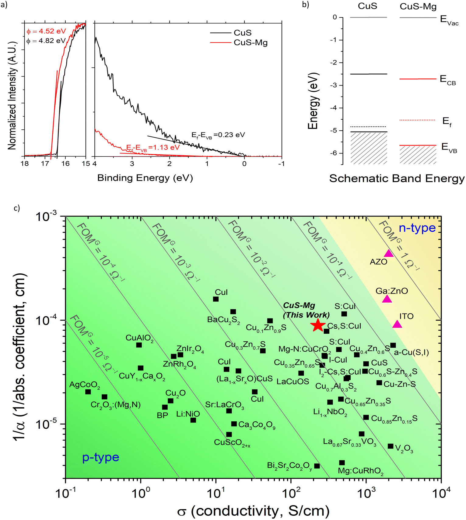 | ||
| Fig. 5 (a) UPS spectra at the secondary electron cut off and valence band region. (b) Schematic band alignment of CuS and CuS–Mg. (c) List of different p-type transparent conducting materials as a function of inverse absorption coefficient at 550 nm and conductivity. The yellow area indicates the region of reported n-type transparent conducting oxides. The grey line indicates FOMG values. | ||
Furthermore, we also compared the performance of our champion CuS–Mg with the p-type TCMs in the literature. Fig. 5(c) shows the relationship between inverse of absorption coefficient and conductivity of various TCMs. The grey lines depicted the FOMG. In addition, Fig. S16 (ESI†) shows the comparison of CuS–Mg with other TCMs based on its transmittance at 550 nm and average sheet resistance with the grey lines depicting the FOMH. The full list is shown in Table S5 (ESI†). Our CuS–Mg shows a comparable high FOMG with the best reported TCMs and therefore highlights the great potential of this materials as a high performing p-type TCM.
Device characteristics using CuS and CuS–Mg
To demonstrate the benefit of Mg-modified CuS in optoelectronic application, a p–n heterojunction diode was fabricated by depositing CdS on top of the p-type CuS film. Ag electrode contacts (∼100 nm) were deposited on both CuS and CdS, resulting in an Ag/CuS/CdS/Ag configuration. Fig. 6(a) shows a comparison of the I–V characteristics of CuS/CdS and CuS–Mg/CdS diodes, with a bias ranging from −3 V to +3 V in logarithmic current. The CuS devices exhibit an ohmic contact behavior, with forward and reverse currents of approximately 1 mA at ±3 V without any rectification behavior. On the other hand, the Mg-modified CuS devices demonstrate rectification with a high rectification ratio of 1.08 × 10⁵ at 3 V biasing condition with a forward turn-on voltage of 0.4 V based on the I–V curve in linear coordinates (see Fig. S17, ESI†). The low turn-on voltage and larger leakage current indicate the characteristic of a Schottky barrier diode, which is shown in a metal–semiconductor junction.65,66 This suggest that the CuS–Mg exhibits metallic/conductor behavior when paired with n-type CdS. On the other hand, although the ohmic behavior in CuS/CdS suggests plausible metallic characteristics of CuS, the absence of semiconducting behavior in CdS indicates the formation of metal–semiconductor junction with poor quality. The shunting problem could have been caused by the rough surfaces of the CuS film. Fig. 6(c), (d) and Fig. S11 (ESI†) show the SEM images of both the plane-view and cross-section view of CuS and CuS–Mg. It can be observed that CuS exhibits a plate-like structure, resulting in a rougher surface compared to CuS–Mg. The CuS–Mg film, on the other hand, appears smoother and more compact due to the amorphization effect of Mg addition. This improved morphology is beneficial for CuS–Mg as it enables uniform growth of subsequent layers and helps avoid the formation of shunting pathways through pinholes. Smaller grains are also observed in the CuS–Mg sample in comparison with the CuS sample. A similar phenomenon was observed in amorphous Cu–Sn–I,67 where a better rectification behavior was observed due to the smoother surface compared to CuI with rougher surface. From the semi-natural logarithm plot of I vs. V, diode ideality factor of 1.6 is extracted from the slope of the linear region. The ideality factor is within 1 to 2 range of typical diode. | ||
| Fig. 6 Current–voltage measurements for CuS/CdS and CuS–Mg/CdS with (a) Ag as the electrode and (b) FTO as the electrode. Schematics of the diode structures are included as insets. Dotted lines represent illumination conditions during the measurements. Plane-view SEM of (c) CuS and (d) CuS–Mg. | ||
Furthermore, the semi-transparent junctions were also prepared by using FTO (fluorine-doped tin oxide) instead of Ag electrodes, resulting in the configuration of FTO/CuS–Mg/CdS/FTO. The transmittance spectra and schematic of band alignment of these films are shown in Fig. S18 (ESI†). As expected, the p–n junction for CuS–Mg exhibits higher transparency compared to CuS, with an average visible transmittance of approximately 66.59% compared to 52.42% for CuS/CdS. The introduction of FTO leads to a decrease in the overall transmittance by approximately 13% for both CuS–Mg/CdS and CuS/CdS stack, resulting in transmittance values of 53.07% and 38.49%, respectively. The band alignment shows that both CuS and CuS–Mg are suitable to form a type II (staggered type) p–n junction.68 From the band diagram, the turn-on voltage can be estimated as the difference between the Fermi levels.69,70 Assuming the Fermi level of CdS is close to its conduction band, the turn-on voltage can be approximated to be 0.4–0.5 eV, which aligns with our experimental observations. In this semi-transparent junction, similar rectifying diode behavior is also observed for CuS–Mg/CdS, albeit with a lower rectification ratio of approximately 8 at 5 V bias, and thus a poorer diode performance, as shown in Fig. 6(b). The devices demonstrate higher current compared to the Ag-electrode devices, which might be attributed to the reduction in the contact resistance between the film and FTO electrode as the FTO cover the film whereas Ag electrode is just a point contact. Additionally, the deposition techniques for the films are different, which affects the junction properties. Another notable observation is that the CuS–Mg device exhibits photodiode behavior, while the CuS/CdS device maintains similar ohmic behavior. When a photodiode with p–n junction is illuminated, the I–V characteristic should be shifted according to the photocurrent and reverse current. By measuring the reverse current response under illumination, it can be deduced that it originates from p–n junction rather than the individual layer of CdS or CuS–Mg. With a −5 V applied bias, the dark reverse leakage current of the diode is only around 3.7 × 10⁻³ A. However, the reverse leakage current rapidly increases to 4.5 × 10⁻² A upon illumination. The reasonably high photo-to-dark-current contrast ratio suggests that the CuS–Mg/CdS junction in this study has the potential as photodetector for UV pressure sensor in soft robotics or smart window applications.
Additionally, we have fabricated photovoltaic devices using our p-type TCMs as one of the electrodes. The full configuration of the device is glass/p-type TCMs/PEDOT:PSS/perovskite/PCBM-BCP/Ag, with the perovskite composition being triple cation perovskite Cs0.05(MA0.17FA0.83)0.95Pb(I0.83Br0.17)3. Both CuS and CuS–Mg show photovoltaic response with average power conversion efficiencies of 1.8% and 3.7%, respectively. The detailed performance parameters, including open-circuit voltage (Voc), short-circuit current (Jsc), and fill factor, are shown in Fig. S19 (ESI†). The CuS–Mg device shows improved performance compared to the CuS device. Optimization in morphology, device structure and uniformity could be done to further improve the performance. Nevertheless, this proof-of-concept device demonstrates that our p-type material can function as electrode in optoelectronic devices.
Conclusion
In conclusion, this study highlights the promising impact of Mg in enhancing the transparency of CuS films, achieved through a high-throughput screening approach using spray pyrolysis. Through the optimization of fabrication parameters for CuS–Mg films, we successfully obtained a figure of merit (FOM) comparable to the high-performing p-type TCMs reported in the literature. The addition of Mg not only increased the transparency of CuS but also induced a more amorphous structure, leading to a smoother surface and demonstrating its potential as an amorphous p-type TCM. The electronic band structure analysis reveals a downward shift of the VBM, leading to an increased band gap and, consequently, enhanced transparency. Importantly, the incorporation of Mg resulted in only a slight reduction in carrier mobility while maintaining a high carrier concentration, ensuring an overall high conductivity. These changes can be primarily attributed to the weakening of p–d coupling at the VBM caused by the incorporation of Mg.Furthermore, our investigation extends beyond CuS films alone. The photodiode utilizing n-type CdS in combination with CuS–Mg demonstrated superior performance than pure CuS. This observation suggests that, with further optimization, the CuS–Mg technology has the potential to serve as a novel p-type TCM with broad applications in transparent electronics and optoelectronic devices such as photodetectors for smart displays, window-integrated electronic circuits and sensors in soft robotics. In conclusion, our study not only presents a valuable contribution to the field but also opens new avenues for advancements in transparent electronics through the seamless integration of high-throughput screening and theoretical validation methodologies.
Author contributions
Conceptualization, S. L. and L. H. W.; methodology, S. L. and Q. S.; validation, S. L. and Q. S.; investigation, S. L., Q. S., P. M., P. W. F. L. and T. S.; formal analysis, S. L., Q. S., P. M., P. W. F. L. and T. S.; resources, Sz. L., G. H. and L. H. W.; writing – original draft, S. L. and Q. S.; writing – review & editing, P. M., P. W. F. L., T. S., Sz. L., G. H. and L. H. W.; visualization, S. L., Q. S., P. M., P. W. F. L. and T. S.; supervision, Sz. L., G. H. and L. H. W.; funding acquisition, L. H. W.Data availability
The data that support the findings of this study are openly available in NTU research data repository DR-NTU (Data) at https://doi.org/10.21979/N9/DPQWT3.Conflicts of interest
There are no conflicts to declare.Acknowledgements
This work is supported by the Singapore Ministry of Education Tier 2 grant (MOE T2EP50120-0008). This research is supported by grants from the National Research Foundation, Prime Minister's Office, Singapore under its Campus of Research Excellence and Technological Enterprise (CREATE) programme. We would like to acknowledge the Facility for Analysis, Characterization, Testing and Simulation, Nanyang Technological University, Singapore, for use of their electron microscopy/X-ray facilities, and the computing resources from National Supercomputing Centre Singapore for DFT calculations.References
- D. S. Ginley and J. D. Perkins, Handbook of transparent conductors, Springer, 2010, pp. 1–25 Search PubMed.
- S. Rahmany and L. Etgar, ACS Energy Lett., 2020, 5, 1519–1531 CrossRef CAS.
- J. Sun and J. Jasieniak, J. Phys. D: Appl. Phys., 2017, 50, 093001 CrossRef.
- P. M. Rajanna, H. Meddeb, O. Sergeev, A. P. Tsapenko, S. Bereznev, M. Vehse, O. Volobujeva, M. Danilson, P. D. Lund and A. G. Nasibulin, Nano Energy, 2020, 67, 104183 CrossRef CAS.
- P. Yilmaz, M. Magni, S. Martinez, R. M. Gonzalez Gil, M. Della Pirriera and M. Manca, ACS Appl. Energy Mater., 2020, 3, 3779–3788 CrossRef CAS.
- D. R. Rosseinsky and R. J. Mortimer, Adv. Mater., 2001, 13, 783–793 CrossRef CAS.
- M. Nikolou, A. L. Dyer, T. T. Steckler, E. P. Donoghue, Z. Wu, N. C. Heston, A. G. Rinzler, D. B. Tanner and J. R. Reynolds, Chem. Mater., 2009, 21, 5539–5547 CrossRef CAS.
- N. Gagrani, K. Vora, C. Jagadish and H. H. Tan, ACS Appl. Mater. Interfaces, 2022, 14, 37101–37109 CrossRef CAS.
- J. Min Lee, H. Yong Jeong, K. Jin Choi and W. Il Park, Appl. Phys. Lett., 2011, 99, 041115 CrossRef.
- Z. Yang, M. Wang, J. Ding, Z. Sun, L. Li, J. Huang, J. Liu and J. Shao, ACS Appl. Mater. Interfaces, 2015, 7, 21235–21244 CrossRef CAS PubMed.
- C.-L. Hsu, K.-C. Chen, T.-Y. Tsai and T.-J. Hsueh, Sens. Actuators, B, 2013, 182, 190–196 CrossRef CAS.
- T. Minami, Thin Solid Films, 2008, 516, 5822–5828 CrossRef CAS.
- S. B. Zhang, J. Phys.: Condens. Matter, 2002, 14, R881 CrossRef CAS.
- A. Zunger, Appl. Phys. Lett., 2003, 83, 57–59 CrossRef CAS.
- L. Hu, R. H. Wei, X. W. Tang, W. J. Lu, X. B. Zhu and Y. P. Sun, J. Appl. Phys., 2020, 128, 140902 CrossRef CAS.
- H. Kawazoe, M. Yasukawa, H. Hyodo, M. Kurita, H. Yanagi and H. Hosono, Nature, 1997, 389, 939–942 CrossRef CAS.
- K. H. Zhang, K. Xi, M. G. Blamire and R. G. Egdell, J. Phys.: Condens. Matter, 2016, 28, 383002 CrossRef.
- J. Zhang, H. Shen, Y. Xu, B. Xu, Y. Feng, J. Ge and Y. Li, Surf. Interfaces, 2021, 26, 101430 CrossRef CAS.
- J. Tirado, D. Ramirez, R. Betancur and F. Jaramillo, Thin Solid Films, 2018, 662, 90–96 CrossRef CAS.
- L. Li, J. Huang, W. Yang, K. Tang, B. Ren, H. Xu and L. Wang, Surf. Coat. Technol., 2016, 307, 1024–1028 CrossRef CAS.
- T. S. Tripathi, J. Lahtinen and M. Karppinen, Adv. Mater. Interfaces, 2018, 5, 1701366 CrossRef.
- X. Xu, J. Bullock, L. T. Schelhas, E. Z. Stutz, J. J. Fonseca, M. Hettick, V. L. Pool, K. F. Tai, M. F. Toney, X. Fang, A. Javey, L. H. Wong and J. W. Ager, Nano Lett., 2016, 16, 1925–1932 CrossRef CAS.
- S. H. Chaki, M. P. Deshpande and J. P. Tailor, Thin Solid Films, 2014, 550, 291–297 CrossRef CAS.
- S. S. Pathak and L. S. Panchakarla, Appl. Mater. Today, 2021, 24, 101152 CrossRef.
- A. Mallick, S. Chattopadhyay, G. De and D. Basak, J. Alloys Compd., 2019, 770, 813–822 CrossRef CAS.
- E. Jose, M. Mohan, M. A. G. Namboothiry and M. C. S. Kumar, J. Alloys Compd., 2020, 829, 154507 CrossRef CAS.
- K. Maeda, N. Kawaida, R. Tsudome, K. Sakai and T. Ikari, Phys. Status Solidi C, 2012, 9, 2271–2274 CrossRef CAS.
- H. Okuyama, K. Nakano, T. M. Takao Miyajima and K. A. Katsuhiro Akimoto, Jpn. J. Appl. Phys., 1991, 30, L1620 CrossRef CAS.
- A. Vij, S. Singh, R. Kumar, S. P. Lochab, V. V. S. Kumar and N. Singh, J. Phys. D: Appl. Phys., 2009, 42, 105103 CrossRef.
- D. Jia, R. S. Meltzer and W. M. Yen, J. Lumin., 2002, 99, 1–6 CrossRef CAS.
- J. Resende, C. Jiménez, N. D. Nguyen and J. L. Deschanvres, Phys. Status Solidi A, 2016, 213, 2296–2302 CrossRef CAS.
- H. Hiramatsu, K. Ueda, H. Ohta, M. Hirano, T. Kamiya and H. Hosono, Appl. Phys. Lett., 2003, 82, 1048–1050 CrossRef CAS.
- E. Arca, K. Fleischer and I. Shvets, Appl. Phys. Lett., 2011, 99, 111910 CrossRef.
- M. Moreira, J. Afonso, J. Crepelliere, D. Lenoble and P. Lunca-Popa, J. Mater. Sci., 2022, 57, 3114–3142 CrossRef CAS.
- K. Ueda, S. Inoue, S. Hirose, H. Kawazoe and H. Hosono, Appl. Phys. Lett., 2000, 77, 2701–2703 CrossRef CAS.
- K. H. Zhang, Y. Du, A. Papadogianni, O. Bierwagen, S. Sallis, L. F. Piper, M. E. Bowden, V. Shutthanandan, P. V. Sushko and S. A. Chambers, Adv. Mater., 2015, 27, 5191–5195 CrossRef CAS.
- S. Sheng, G. Fang, C. Li, Z. Chen, S. Ma, L. Fang and X. Zhao, Semicond. Sci. Technol., 2006, 21, 586 CrossRef CAS.
- L. Cheng, Q. Xiang, Y. Liao and H. Zhang, Energy Environ. Sci., 2018, 11, 1362–1391 RSC.
- G. Haacke, J. Appl. Phys., 1976, 47, 4086–4089 CrossRef CAS.
- R. G. Gordon, MRS Bull., 2000, 25, 52–57 CrossRef CAS.
- L. Hu, R. Wei, J. Yan, D. Wang, X. Tang, X. Luo, W. Song, J. Dai, X. Zhu, C. Zhang and Y. Sun, Adv. Electron. Mater., 2018, 4, 1700476 CrossRef.
- L. Farrell, K. Fleischer, D. Caffrey, D. Mullarkey, E. Norton and I. Shvets, Phys. Rev. B: Condens. Matter Mater. Phys., 2015, 91, 125202 CrossRef.
- H. Hiramatsu, K. Ueda, H. Ohta, M. Hirano, T. Kamiya and H. Hosono, Appl. Phys. Lett., 2003, 82, 1048–1050 CrossRef CAS.
- X. Cai, F. P. Sabino, A. Janotti and S.-H. Wei, Phys. Rev. B, 2021, 103, 115205 CrossRef CAS.
- T. S. Tripathi and M. Karppinen, Adv. Electron. Mater., 2017, 3, 1600341 CrossRef.
- S. Sheng, G. Fang, C. Li, S. Xu and X. Zhao, Phys. Status Solidi A, 2006, 203, 1891–1900 CrossRef CAS.
- J. Chen, W. Cranton and M. Fihn, Handbook of visual display technology, Springer, 2016 Search PubMed.
- T. Jun, J. Kim, M. Sasase and H. Hosono, Adv. Mater., 2018, 30, 1706573 CrossRef.
- S. Li, Y. Zhang, W. Yang and X. Fang, Adv. Mater. Interfaces, 2019, 6, 1900669 CrossRef.
- B. Zhang, G. Xia, W. Chen, Q. Gu, D. Sun and X. Yu, ACS Nano, 2018, 12, 12741–12750 CrossRef CAS PubMed.
- M. C. Biesinger, Surf. Interface Anal., 2017, 49, 1325–1334 CrossRef CAS.
- N. Karikalan, R. Karthik, S.-M. Chen, C. Karuppiah and A. Elangovan, Sci. Rep., 2017, 7, 2494 CrossRef PubMed.
- J. C. Fuggle, Surf. Sci., 1977, 69, 581–608 CrossRef CAS.
- S. Ardizzone, C. L. Bianchi, M. Fadoni and B. Vercelli, Appl. Surf. Sci., 1997, 119, 253–259 CrossRef CAS.
- Ş. Süzer, Appl. Spectrosc., 2000, 54, 1716–1718 CrossRef.
- A. Pedone, G. Malavasi, M. C. Menziani, U. Segre and A. N. Cormack, J. Phys. Chem. C, 2008, 112, 11034–11041 CrossRef CAS.
- A. Morales-García, A. L. Soares, Jr., E. C. Dos Santos, H. A. de Abreu and H. A. Duarte, J. Phys. Chem. A, 2014, 118, 5823–5831 CrossRef PubMed.
- C. Li, P. Gong, J. Zheng, M. Zhao, R. Wei, W. Cheng, L. Hu, W. Song, X. Zhu and Y. Sun, Adv. Opt. Mater., 2022, 10, 2102559 CrossRef CAS.
- R.-S. Yu and H.-H. Yin, Thin Solid Films, 2012, 526, 103–108 CrossRef CAS.
- H. Peng, A. Zakutayev, S. Lany, T. R. Paudel, M. d'Avezac, P. F. Ndione, J. D. Perkins, D. S. Ginley, A. R. Nagaraja and N. H. Perry, Adv. Funct. Mater., 2013, 23, 5267–5276 CrossRef CAS.
- S. Chen, T. Kuo, Y. Lin and H. Lin, Thin Solid Films, 2011, 519, 4944–4947 CrossRef CAS.
- M. Adelifard, H. Eshghi and M. M. Bagheri Mohagheghi, Opt. Commun., 2012, 285, 4400–4404 CrossRef CAS.
- I. Mazin, Phys. Rev. B: Condens. Matter Mater. Phys., 2012, 85, 115133 CrossRef.
- H. Ning, Y. Zeng, S. Zuo, S. V. Kershaw, Y. Hou, Y. Li, X. Li, J. Zhang, Y. Yi, L. Jing, J. Li and M. Gao, ACS Nano, 2021, 15, 873–883 CrossRef CAS PubMed.
- A. Tombak, M. Benhaliliba, Y. S. Ocak and T. Kiliçoglu, Results Phys., 2015, 5, 314–321 CrossRef.
- T. Hashizume, J. Kotani and H. Hasegawa, Appl. Phys. Lett., 2004, 84, 4884–4886 CrossRef CAS.
- H. Wu, L. Liang, X. Wang, H. Zhang, J. Bao and H. Cao, Appl. Phys. Lett., 2021, 118, 222107 CrossRef CAS.
- M. Razeghi, Fundamentals of Solid State Engineering, Springer, US, 2009 Search PubMed.
- S. M. Sze and K. K. Ng, Physics of Semiconductor Devices, 2006, pp. 77–133 DOI:10.1002/9780470068328.ch2.
- S. M. Sze and K. K. Ng, Physics of Semiconductor Devices, 2006, pp. 134–196 DOI:10.1002/9780470068328.ch3.
Footnote |
| † Electronic supplementary information (ESI) available. See DOI: https://doi.org/10.1039/d4mh01501k |
| This journal is © The Royal Society of Chemistry 2025 |