
Highly efficient and stable hybrid quantum-dot light-emitting field-effect transistors†
Penghui
He
,
Linfeng
Lan
 *,
Caihao
Deng
,
Jian
Wang
,
Junbiao
Peng
and
Yong
Cao
*,
Caihao
Deng
,
Jian
Wang
,
Junbiao
Peng
and
Yong
Cao
State Key Laboratory of Luminescent Materials and Devices, South China University of Technology, Guangzhou 510640, China. E-mail: lanlinfeng@scut.edu.cn
First published on 6th July 2020
Abstract
Light-emitting field-effect transistors (LETs) have drawn much attention for their special capability of combining switching and electroluminescence capacity in a single device. Herein, we report a colour-saturated, high-efficiency red quantum-dot hybrid light-emitting field-effect transistor (QD-HLET) with a solution-processed InScO/ZnO-nanoparticle heterojunction channel layer and a deep-level organic hole transport layer (HLT). The red QD-HLET exhibits a field-effect mobility of 3.1 cm2 V−1 s−1 with an on/off ratio of ∼105, a maximum brightness of 145![[thin space (1/6-em)]](https://www.rsc.org/images/entities/char_2009.gif) 000 cd m−2 with a peak external quantum efficiency (EQE) of 22.8% and low efficiency roll-off (an EQE of 17.0% at a brightness of 100000 cd m−2). In addition, the operating stability of the HLET is investigated by monitoring the time-dependent change in the brightness of the QD-HLET under various VGS, while an operational lifetime of more than 153000 hours at 100 cd m−2 is achieved. A comprehensive study on the electrical and optical characteristics of the red QD-HLET under different operation modes is conducted, and an operation model is proposed.
000 cd m−2 with a peak external quantum efficiency (EQE) of 22.8% and low efficiency roll-off (an EQE of 17.0% at a brightness of 100000 cd m−2). In addition, the operating stability of the HLET is investigated by monitoring the time-dependent change in the brightness of the QD-HLET under various VGS, while an operational lifetime of more than 153000 hours at 100 cd m−2 is achieved. A comprehensive study on the electrical and optical characteristics of the red QD-HLET under different operation modes is conducted, and an operation model is proposed.
New conceptsIn this manuscript, we demonstrate high-performance hybrid quantum-dot light-emitting field-effect transistors (QD-HLETs), which combine the high electron mobility of the InScO/ZnO heterostructure and high luminous efficiency of the core–shell QD emitting material. A field-effect mobility of 3.1 cm2 V−1 s−1 and a peak EQE of 22.8% are obtained. To the best of our knowledge, the efficiency of the red QD-HLET is higher than those of any kinds of LETs, and even higher than those of any top-emitting QLEDs ever reported. We find that the device performances can be modified by simply optimizing the thickness of ZnO. And, interestingly, the device demonstrates different optical and electrical characteristics under different operation modes, which is beneficial to understand the operational mechanism of the LET and maintain a high EQE in a wide range of current density. In addition, it is the first time that the operating stability of an HLET is investigated by monitoring the time-dependent change in the brightness of the QD-HLET under various VGS. Corresponding to that, the estimated operational lifetime at 100 cd m−2 is more than 153000 hours.
|
Introduction
As a novel multifunctional three-terminal active device which combines the functions of electroluminescence of an organic/quantum-dot light-emitting diode (OLED/QLED) and current modulation with the gate voltage of a thin-film transistor (TFT) in a single device,1–3 light-emitting field-effect transistors (LETs) have aroused growing interest for potential applications in display pixels, optical communication devices, electric pump lasers, etc.4–7 During the past few years, great efforts have been made to improve the performances of LETs with various device structures,8–19 such as multilayer,3,6,15 vertical,11,19 unsymmetrical-source/drain,12,18 and split-gate8 structures. For single-layer LETs, it is almost impossible to concurrently improve the field-effect mobility and the luminous efficiency, because the compact π–π conjugate stacking for providing high carrier mobility would result in severe exciton quenching.20 Hence, multilayer structures are employed to take advantage of both the high luminous efficiency of emitting materials and high mobility of channel materials. Capelli et al.3 demonstrated an organic LET (OLET) with a p-channel/emitter/n-channel trilayer structure and attained a peak external quantum efficiency (EQE) of ∼5%, which is more than 100 times that of the equivalent OLED. Although the mobility is low and the EQE is still lower than the state-of-the-art OLEDs, it proves for the first time that LETs can be more efficient than the equivalent light-emitting diodes.To improve the field-effect mobility of LETs, hybrid light-emitting field-effect transistors (HLETs) with an organic emitting layer and inorganic semiconductor channel layer are proposed. Compared to most organic semiconductor channel materials, inorganic metal oxide (MO) semiconductors have the advantages of higher electron mobility, better uniformity, better chemical and electrical stability, and higher transparency for visible light.21–23 Moreover, MO films, which can be prepared by solution processes using precursor solutions, can hardly be etched by most of the organic solvents typically used for dissolving organic materials, which benefits cost-efficient solution-processed multilayer devices with intermixing-free interfaces.17,18 However, the Fermi levels (EF) for most MO semiconductors are deep, which will form large carrier-injection barriers with organic emitting materials that have shallow lowest unoccupied molecular orbitals (LUMOs), and lead to low luminous efficiency and a narrow emitting area.
Compared to organic emitting materials, colloidal quantum dots (QDs) have deeper LUMO levels close to the EF of MO semiconductors.24,25 Liu et al.19 report a QD-HLET with a vertical MO channel, but the vertical channel causes a large off-current (Ioff) and low on/off ratio (only about 10, judging from the output curves). In our previous work, we demonstrated a QD-HLET with a solution-processed MO semiconductor channel and a QD emitting layer, and attained a mobility of 0.8 cm2 V−1 s−1 and a maximum EQE of 8.7%.17 Although the overall performance is better than those of most LETs, the EQE is still lower than the equivalent QLEDs, and the mobility is not high enough for practical applications.26–32
Herein, we demonstrate a red QD-HLET with high mobility and good electroluminescence performance that is comparable to the state-of-the-art quantum-dot light-emitting diodes (QLEDs) by using a solution-processed InScO/ZnO-nanoparticle heterojunction channel layer, a colloidal core/shell QD emitting layer and a deep-level organic hole transport layer (HTL). And, interestingly, the device demonstrates different optical and electrical characteristics when under different operation modes, which is beneficial to research the operational mechanism of the QD-HLET. In addition, the operating stability of the HLET is investigated by monitoring the time-dependent change in the brightness of the QD-HLET under various VGS. A comprehensive study on the electrical and optical characteristics as well as the operation stability of the QD-HLETs under different operation modes is carried out. On the basis of the experiment and calculation results, an operation model for the HLETs is proposed.
Results and discussion
Characteristics of TFTs
Firstly, the influence of the heterojunction channel on the electrical characteristics of the TFTs was investigated. For comparison, TFTs with a single layer of ZnO-nanoparticles or InScO were also prepared. The device structures of the TFTs with solution-processed ZnO-nanoparticle (50 nm), InScO (3.4 nm) and InScO/ZnO-nanoparticle heterojunction (with optimized thicknesses of 3.4 nm/50 nm) channels are shown in Fig. 1a–c, respectively. The three devices share the same bottom-gate and top-contact structure. For the heterojunction TFT, a uniformly continuous InScO film was covered by a thick ZnO-nanoparticle layer with a clear interface, as shown in Fig. S1b (ESI†). The corresponding transfer curves of the TFTs with different channels are shown in Fig. 1d–f. All devices exhibit typical n-type field-effect characteristics. The TFT with the ZnO-nanoparticle channel exhibits low electron mobility (0.003 cm2 V−1 s−1), which is ascribed to the large boundary gaps between adjacent nanoparticles (see the TEM images in Fig. S1b, ESI†). The TFT with the single InScO channel exhibits much higher mobility of 1.5 cm2 V−1 s−1 and less hysteresis in the transfer curves between forward and reverse sweeps compared to the one with the ZnO-nanoparticle channel. The InScO/ZnO-nanoparticle heterojunction TFT exhibits the highest mobility of 2.7 cm2 V−1 s−1 and almost no hysteresis with an on/off current ratio as high as ∼107. The mobility enhancement of the InScO/ZnO-nanoparticle heterojunction TFT is attributed to the large carrier density difference between the InScO film (9.2 × 1019 cm−3) and the ZnO-nanoparticle film (2.0 × 1014 cm−3). In this case, most carriers are confined to the InScO film, and the ZnO-nanoparticle film acts as a protection layer to prevent the InScO film from being doped by water/oxygen molecules or being damaged when depositing QD layers.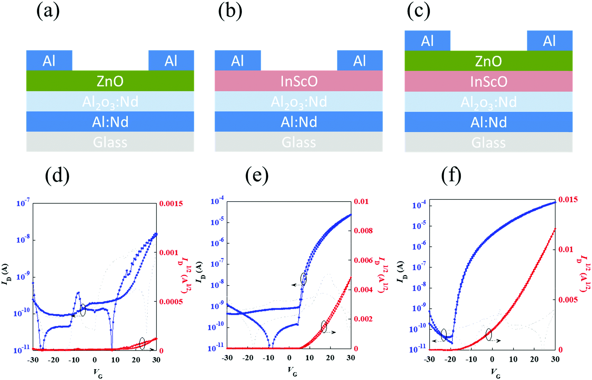 | ||
| Fig. 1 (a–c) The device structure of the TFTs with solution-processed ZnO-nanoparticle, InScO and InScO/ZnO-nanoparticle heterojunction (with optimized thicknesses of 3.4 nm/50 nm) channels by spin-coating, respectively. (d–f) The transfer characteristics of TFTs with different channels measured at VDS = 30 V and VGS = −30 to 30 V. | ||
The characteristics of the QD-HLET
The QD-HLETs were fabricated with a bottom-gate, top-emitting and asymmetric non-planar source/drain configuration (Fig. 2a), which consists of an Al:Nd (3% Nd) gate reflective electrode and an anodic Al2O3:Nd dielectric layer, followed by spin-coating of the InScO (precursor solution)/ZnO-nanoparticle (colloid solution) heterojunction channel and QD (colloid solution) emitter layer in sequence. After that, an organic HTL (4,4′,4′′-tris(carbazol-9-yl)triphenylamine, TCTA) was deposited on the QD emitting layer by vacuum thermal evaporation. Finally, asymmetric non-planar Al and MoOX/Au electrodes were employed to enhance the injection of electrons and holes.18Fig. 2c and d show the scanning transmission electron microscopy (STEM) images of the QD-HLET with different magnifications (the corresponding element distribution maps are shown in Fig. 2e). A distinct stack of functional layers and clear interfaces are observed, revealing that the functional layers are hardly damaged by subsequent solvents. Furthermore, 2–3 layers of QDs are uniformly covered on the ZnO-nanoparticle film, and almost no particle aggregation is found for both the QD and ZnO-nanoparticle films, indicating good dispersion of the suspensions.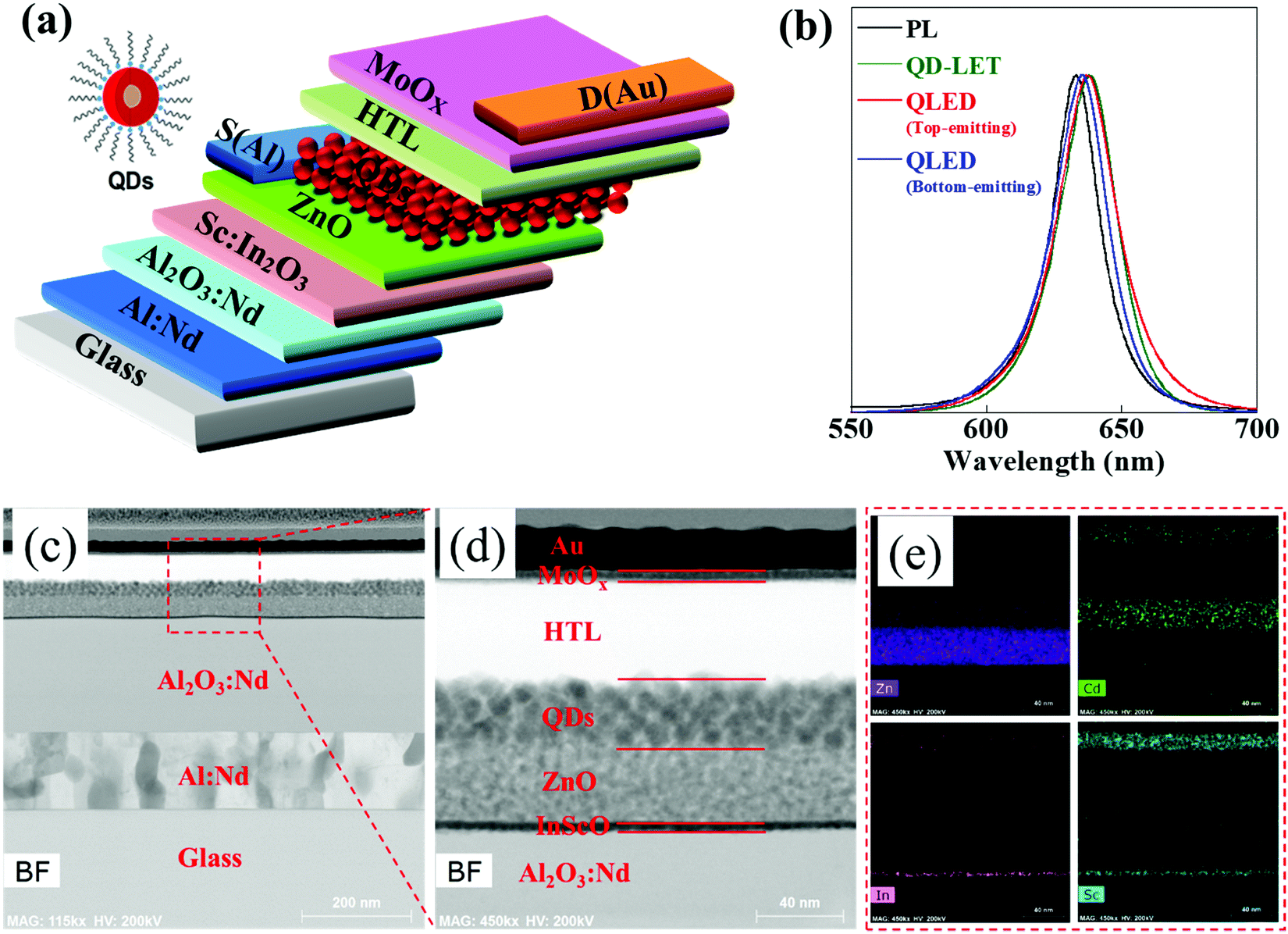 | ||
| Fig. 2 (a) Device structure of the QD-HLET. (b) PL spectrum of the red QD film and normal EL spectra of the QD-HLET, bottom-emitting QLED and equivalent top-emitting QLED. (c and d) STEM images with different magnifications of the QD-HLET. (e) EDS mapping image of the QD-HLET. | ||
Fig. 2b shows the photoluminescence (PL) spectrum of the QD film and the electroluminescence (EL) spectra of the red QD-HLET, the bottom-emitting QLED and the equivalent top-emitting QLED (using the equivalent device construction with a uniform functional layer, and the structures of the QLEDs are shown in Fig. S2, ESI†). Colour-saturated deep-red EL emission with an emission peak of 638 nm and a full-width at half-maximum (FWHM) of 25 nm is observed from the whole drain electrode of the red QD-HLET. The EL spectrum of the red QD-HLET corresponds to Commission Internationale de l′Eclairage (CIE) colour coordinates of (0.70, 0.30), which is ideal in display applications, and is consistent with the equivalent top-emitting QLED except lower emission at the root segment of the spectra. Compared to the PL spectrum of the QD film, the EL emission peak red shifts from 634 nm to 638 nm, which is mainly attributed to the electric-field-induced Stark effect and the microcavity effect,30,33 as discussed later.
Fig. 3a shows the electrical and optical transfer curves of the red QD-HLET with the TCTA HTL. The drain voltage (VDS) was held at various voltages of 10, 20, and 30 V, and the gate voltage (VGS) swept from −50 to 30 V at each VDS. The device exhibits typical unipolar n-channel transistor characteristics with an electron field-effect mobility of 3.1 cm2 V−1 s−1 and a saturation current as high as 1.3 × 10⁻³ A μm−1 at VDS = 30 V, which indicates that the abundant electrons injected from the source can cross the channel speedily and recombine with holes injected from the drain in the QD emitting layer. Meanwhile, the device exhibits an on/off ratio of ∼105 corresponding to an off-state current as low as 10−9 A μm−1 and a gate leakage current as low as 10−9 A (Fig. S3, ESI†). The more negative threshold voltage of the QD-HLET compared to that of the TFT is attributed to the QD/HTL/MoOx stack layers, which block the oxygen molecules in the air from adsorbing onto the surface of the back channel. The higher off-state current of the QD-HLET compared to that of the TFT is caused by the HTL (TCTA, hole mobility ∼2 × 10⁻⁵ cm−2 V−1 s−1), which provides another carrier transport path between the source and drain.
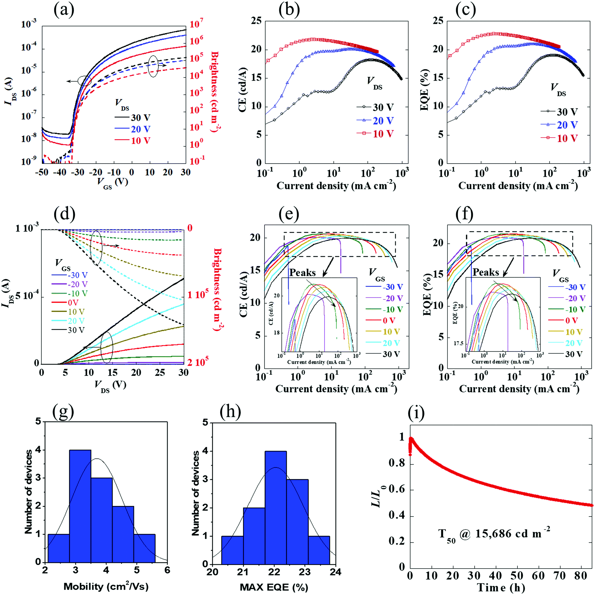 | ||
| Fig. 3 (a) The electrical and optical transfer characteristic curves, (b) CE versus current density curves and (c) EQE versus current density curves of the QD-HLET (VDS was held at different voltages of 10, 20, and 30 V, and VGS swept from −50 to 30 V at each VDS). (d) The electrical and optical output characteristic curves, (e) current efficiency versus current density curves and (f) corresponding EQE versus current density curves of the QD-HLETs (VGS was held at different voltages between −30 and 30 V in steps of 10 V, and VDS swept from 0 to 30 V at each VGS); the insets of (e and f) are the corresponding amplified curves. (g and h) The histogram of the peak mobility and max EQE for 11 devices, respectively. (i) The operating lifetime curves of the red QD-HLET at a constant current density of 71 mA cm−2, corresponding to an initial luminance of 15686 cd m−2. | ||
It can be seen from Fig. 3a and Fig. S4 (ESI†) that the red QD-HLET exhibits excellent optical modulation with the gate voltage, with an on/off brightness ratio greater than 106. There is no luminescence from the QD-HLET when VGS < Von (turn-on voltage, defined as the VGS when drain/source current begin to increcse rapidly) due to the low off-state current and gate leakage current. However, the current density and brightness increase steeply once VGS > Von, and a maximum brightness as high as 145000 cd m−2 is obtained at VGS = 30 V and VDS = 30 V. As shown in Fig. 3b and c the transfer measurements at various VDS yield significantly different luminous efficiency curves. The device demonstrates higher current efficiency (CE) under lower VDS in particular with low current density. A peak external quantum efficiency (EQE) as high as 22.8% with a corresponding peak CE as high as 21.8 cd A−1 is achieved at VDS = 10 V with a brightness of 500 cd m−2 for this device. To the best of our knowledge, it is the highest efficiency (EQE) for all kinds of LETs. However, the peak EQEs are 21.1% and 19.0% at a brightness of 6500 cd m−2 (VDS = 20 V) and 23000 cd m−2 (VDS = 30 V), respectively. The slight decline of the peak EQE with increasing VDS is mainly attributed to more exciton quenching and nonradiative recombination induced by a stronger electric field and higher current density.34–36 In addition, a high EQE of more than 20% is maintained in a wide current density range of 0.3–193 mA cm−2, corresponding to a brightness range of 60–37000 cd m−2. It is worth noting that the QD-HLET exhibits low efficiency roll-off. An EQE as high as 15.5% is attained even at a current density as high as ∼1000 mA cm−2, corresponding to a brightness of ∼145000 cd m−2, which is promising for high-power applications.26Fig. 3g and h show the distributions of the field-effect mobility and the maximum EQE for 11 QD-HLETs fabricated at different times, respectively. The mobility distribution range is 2.6–5.3 cm2 V−1 s−1, and the EQE distribution range is 20.5–23.2%, which show good reproducibility. By contrast, the equivalent top-emitting QLED and the bottom-emitting QLED (see Fig. S2, ESI†) exhibit a peak CE of only 8.6 and 10.2 cd A−1 (corresponding to a peak EQE of 9.0% and 9.0%), respectively, with serious efficiency roll-off (see Fig. S5, ESI†). The EQE of the equivalent top-emitting QLED steeply declines to 50% of the peak EQE at a brightness of 35000 cd m−2. To the best of our knowledge, the EQE of the red QD-HLETs with the InScO/ZnO-nanoparticle heterojunction channel is higher than those of any other kinds of LETs (Table S1, ESI†),3,15–19,37–39 and even higher than those of any top-emitting QLEDs ever reported (Table 1),30,31 and close to those of the state-of-the-art bottom-emitting QLEDs.26–29,32 As is known, top-emitting architectures are more preferred for display applications, because light transmitting from the top contact can improve the aperture ratio of the displays greatly and allow the fabrication of QLEDs on opaque or semitransparent flexible substrates like polyimide (PI), which is the main kind of substrate for commercial flexible displays.40 Hence, the QD-HLET shows its tremendous potential for high resolution and flexible displays.
| Device types | λ max (nm) | FWHM (nm) | EQEmax (%) | EQE at 50000 cd m−2 (%) |
L max (cd m−2) | T 50 at 100 cd m−2 (h) | Ref. |
|---|---|---|---|---|---|---|---|
| TE, top-emitting; N/A, not available. | |||||||
| QD-HLET | 638 | 25 | 22.8 | 19.5 | 145000 |
153000 |
This work |
| TE-QLED (equivalent) | 638 | 25 | 9 | N/A | 35000 |
28000 |
This work |
| TE-QLED | 632 | 32 | 12.5 | N/A | 79000 |
N/A | 30 |
Fig. 3d shows the electrical and optical output curves of the red QD-HLET (VGS was held at different voltages between −20 and 30 V in steps of 10 V, and VDS swept from 0 to 30 V at each VGS). The device shows a distinct “crowded” effect at VDS < 5 V, which is attributed to the increase of contact resistance after insertion of QD/TCTA/MoOX layers between the ZnO-nanoparticles and drain electrode. The device exhibits a brightness turn-on voltage for VDS (VDon, defined as the VDS when the brightness of the devices is 1 cd m−2) of about 2.4 V and a distinct carrier injection start point, which is in accordance with the diode characteristic of QLEDs (Fig. S5 and S6, ESI†).24 In addition, the output current and brightness increase with increasing VGS, suggesting that the electron concentration in the heterostructure channel can be modulated well by VGS. Interestingly, there are significant differences in the CE–current density curves for different VGS (Fig. 3e), suggesting a different electron/hole injection rate under different VGS, as discussed later.
In addition, the operational lifetime, which is an important indicator for photoelectric devices in practical applications, has not been reported yet for LETs. In this study, the operational lifetime of the red QD-HLET was evaluated by testing the brightness as a function of time, as shown in Fig. 3i. T50 (defined as the time at which the device luminance decreases to half of the initial luminance (L0)) for the red QD-HLET is 78 h, which is measured at a constant drain current density of 71 mA cm−2 and a constant VGS of 5 V with an initial luminance of 15686 cd m−2. By using the relation Ln0T50 = const. (assuming an acceleration factor n = 1.5), T50 for the red QD-HLET at 100 cd m−2 is predicted to be ∼153000 h. By contrast, T50 for the equivalent red QLED (top-emitting configuration, see Fig. S3b, ESI†) measured at a constant current density of 71 mA cm−2 is 28000 h at 100 cd m−2 (see Fig. S5c, ESI†). The great improvement in the lifetime of the red QD-HLET compared to the equivalent top-emitting red QLED is mainly attributed to more balanced electron and hole concentrations,24,41 which can be modulated by VGS and VDS, respectively. The detailed mechanisms will be discussed in the following section.
Operational mechanism for QD-HLETs
In an ideal QLET or QLED, the emitting layer should have unity photoluminescence quantum yield (PLQY), and the electron transport layer (ETL) should have a shallower lowest unoccupied molecular orbital (LUMO) level than the emitting layer, while the HTL should have a deeper highest occupied molecular orbital (HOMO) level than the emitting layer.3 In this work, high luminous efficiency red core–shell QDs with a solution PLQY of 90% are employed, but they have a deep LUMO level of −4.0 eV.29 The energy band levels of the InScO and ZnO-nanoparticle films can be derived from the ultraviolet photoelectron spectroscopy (UPS) and UV-visible absorption spectroscopy measurements, as shown in Fig. S7 (ESI†). The energy level diagram of the QD-HLET is depicted in Fig. 4c. The CBM of the ZnO-nanoparticles (−4.0 eV) is very close to the LUMO level of the QDs, resulting in more effective injection of electrons (Fig. S7 and S8, ESI†). In addition, the CBM offset between InScO and the ZnO-nanoparticles can be neglected, so there is almost no barrier between InScO and the ZnO-nanoparticles, which facilitates electron injection. The relatively thick ZnO-nanoparticle layer keeps the QDs away from the accumulation layer of electrons, which reduces the exciton quenching induced by high electron concentration. The HOMO of TCTA (−5.9 eV) provides efficient injection of holes into the QD emitting layer.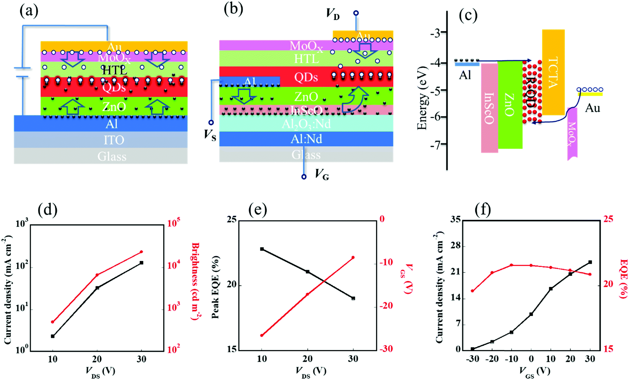 | ||
| Fig. 4 The schematic of the operating mechanism of the top-emitting (a) QLEDs and the (b) QD-HLETs with electrons accumulated and confined in the InScO layer. (c) Energy level diagram of the QD-HLETs. (d) The current density and brightness of the peak EQE as a function of VDS for the transfer characteristic of the red QD-HLET. (e) The peak EQE and corresponding VGS for the transfer characteristic of the red QD-HLET with different VDS. (f) The peak EQE and corresponding current density as a function of VGS for the output characteristic of the red QD-HLET. | ||
However, there are some significant differences in the operating mechanism between the QD-HLET and QLED (see Fig. 4a and b). For the two-terminal QLEDs, the electrons and holes are injected from two electrode, the cathode and anode, respectively. Charge carrier balance in the emitting layer is difficult to achieve, because ideal ETLs and HTLs are difficult to find and their energy levels will change under different electric fields. It means that the carrier balance of the QLEDs will be broken under different applied voltages. In contrast, as a three-terminal active device, the QD-HLET has the advantage of tuning the carriers continuously with the gate voltage so that the charge carriers can be balanced simply by adjusting the gate voltage. When VGS is lower than the turn-on voltage (Von), the electrons in the channel are depleted, so almost no electrons are injected into the QD emitting layer. As a result, the device exhibits an off state with low drain current and almost no luminance. However, when VGS > Von, electrons are generated and accumulated in the channel, and are injected into the QD emitting layer by applying a positive VDS, and then recombine with the holes injected from the drain electrode. The number of electrons in the channel can be controlled by VGS, so balanced electrons and holes can be achieved by adjusting VGS (see Fig. S9, ESI†).
It can be derived from the definition of the mobility (μ = v/E, where v is the velocity of carriers, and E is the electric field strength) that the current density (J) can be expressed as
| J = n·q·v = n·q·μ·E | (1) |
Interestingly, the influence of the excess electrons/holes on the performance of the QD-HLETs can be investigated by simply changing VGS and VDS. The relations between the luminous efficiency and current density at different VDS (Fig. 3b and c) are analyzed in detail. The current efficiency firstly increases and then decreases with increasing current density for all VDS. However, at a low current density, the efficiency at lower VDS is higher than that with higher VDS (at a fixed current density), e.g., the device has an EQE of 22.0%, 18.5%, and 11.5% at a current density of 1 mA cm−2 under a VDS of 10 V, 20 V, and 30 V, respectively. It means that at lower current density, increasing hole concentration (increasing VDS) causes excess holes, leading to a decrease of the efficiency.35,36 At higher current density, the electrons and holes become more and more balanced as VDS increases, so the efficiency increases. For each VDS of 10 V, 20 V, and 30 V, the peak EQE is achieved at a current density of 2.3, 32.4, and 127.2 mA cm−2, respectively, corresponding to a brightness of 502.3, 6537.5, and 23172.0 cd m−2, and a VGS of −26.5, −17.0, and −8.5 V (Fig. 4d and e). The increase of the peak EQE current at larger VDS is ascribed to the fact that larger VDS provides more hole charges, and requires more positive VGS to increase the electron concentration to balance the charge concentration.35
As shown in Fig. 3e and f, at each VGS, the efficiency firstly increases and then decreases with the current density. That means that at a fixed electron concentration the hole injection is weak at low VDS, leading to an excess of electrons. As the hole injection is enhanced (VDS increases), the electrons and holes become more and more balanced until a peak efficiency is reached (see the insets of Fig. 3e and f); further enhancing the hole injection leads to an excess of holes and in turn decreases the efficiency. More interestingly, the efficiency peaks shift toward the positive direction as VGS increases (the insets of Fig. 3e and f and Fig. 4f). It means that more holes (higher VDS) are required to balance the electrons due to the higher electron concentration at higher VGS. Simultaneously, the device exhibits a higher efficiency at more negative VGS when the current density is low, but exhibits a higher efficiency at more positive VGS when the current density is high (compared at a fixed current density, Fig. 3e and f). Surprisingly, there is a brightness peak in the saturation regime (the brightness drops when VDS > 20 V, see Fig. S10, ESI†), while the current is almost unchanged, which corresponds to the rapid CE decrease with current density, because of nonradiative recombination induced by excess holes due to the electron concentration being limited by VGS. This is further evidence for the QD-HLET being superior to the QLED, because the QD-HLET can change the brightness (as well as efficiency) at a constant current, while it is impossible for the QLED.
Mechanisms for the long lifetime
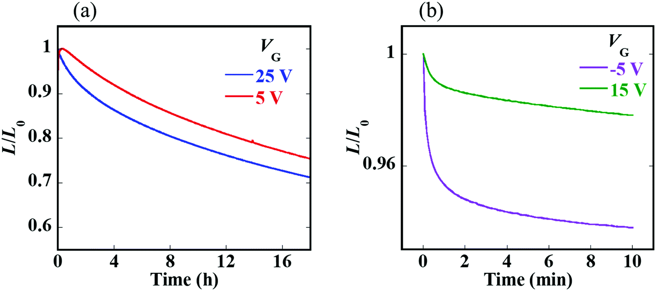
Balanced charge concentration not only enhances the luminance efficiency, but also improves the lifetimes of QLEDs/QD-HLETs. The operational lifetime has been extensively studied in inorganic–organic hybrid QLEDs. It has been reported that the operational instability results from the nonradiative Auger recombination processes of negative trions (two electrons and one hole, X−) in the QDs induced by the accumulation of excess charge carriers owing to imbalanced injection in running devices, the exciton quenching induced by Joule heating, or the irreversible physical damage of the organic HTL caused by the excess electron leakage toward the HTLs and creating nonradiative recombination centers.36,42–44 Likewise, the accumulation of excess holes in QDs escalates the probability of the nonradiative Auger recombination of positive trions (one electron and two holes, X+),45 and some of the excess holes may move toward the ETLs (herein ZnO) and be captured by oxygen vacancies (VO) of the ZnO-nanoparticle film due to the large amount of VO subgap states above the VBM of metal-oxide semiconductors.46 When a VO captures a hole, it changes to a doubly charged oxygen vacancy (VO2+), which cannot fully recover unless extra annealing steps are carried out.In contrast with two-terminal devices like QLEDs, the three-terminal QD-HLET, whose electron concentration can be modulated by the gate voltage, is an ideal platform for studying the operational stability of photoelectric devices based on QDs. Fig. 5a shows the time-dependent change in the brightness of the red QD-HLET at different VGS with a constant current density of 71 mA cm−2. T80 is 13 h and 8 h when VGS is 5 V and 25 V, respectively, suggesting that the operational lifetime of the QD-HLET can be modified by VGS. The device luminance falls more rapidly at higher VGS, which is mainly attributed to excess electron concentration in the channel, which leads to nonradiative Auger recombination and irreversible physical damage of the organic HTL.43,44Fig. 5b compares the luminance decay over time of the red QD-HLET under a loop test of 10 min between VGS of −5 V and 15 V. When VGS is at −5 V, the device exhibits more rapid fall-off during the early few minutes. Because the electron concentration is limited under a negative VGS of −5 V, a number of positive trions are formed in the QD layer, causing inferior operational stability.45 Thus, the balanced charge concentration is one of the reasons for the great improvement in the lifetime of the QD-HLETs compared to the equivalent QLEDs.
 | ||
| Fig. 5 (a) The operational lifetime of the red QD-HLET tested at different VGS and a constant current density of 71 mA cm−2. (b) The luminance as a function of time for the red QD-HLET with a loop test between −5 V and 15 V of VGS at a constant current density of 71 mA cm−2. | ||
Influence of different ETLs
As mentioned above, the insertion of a thick ZnO-nanoparticle layer between the InScO layer and QD layer confines the field-induced electron carriers in the InScO layer, and thus decreases the exciton quenching induced by high electron concentration and surface defects without passivation. The QD-HLET without ZnO-nanoparticles exhibits a much lower operational lifetime, in which T50 is only 2 hours with an initial brightness of 670 cd m−2 at a constant current density of 71 mA cm−2 (Fig. S11, ESI†).In addition, the thick ZnO-nanoparticle layer may have an effect on the microcavity effect, because the QD-HLETs are a top-emitting architecture, in which the emission layers are sandwiched between a reflective bottom electrode (gate) and a semi-transparent top electrode (drain). By optimizing the cavity length, light reflected by the top electrode and light reflected by the bottom electrode interfere with each other. As a result, the emission can be enhanced or weakened. Generally, wide-angle interference and multiple-beam interference take place (see Fig. S12, ESI†), and the corresponding resonant wavelength of the microcavity can be expressed with the equations30,31
 | (2) |
 | (3) |
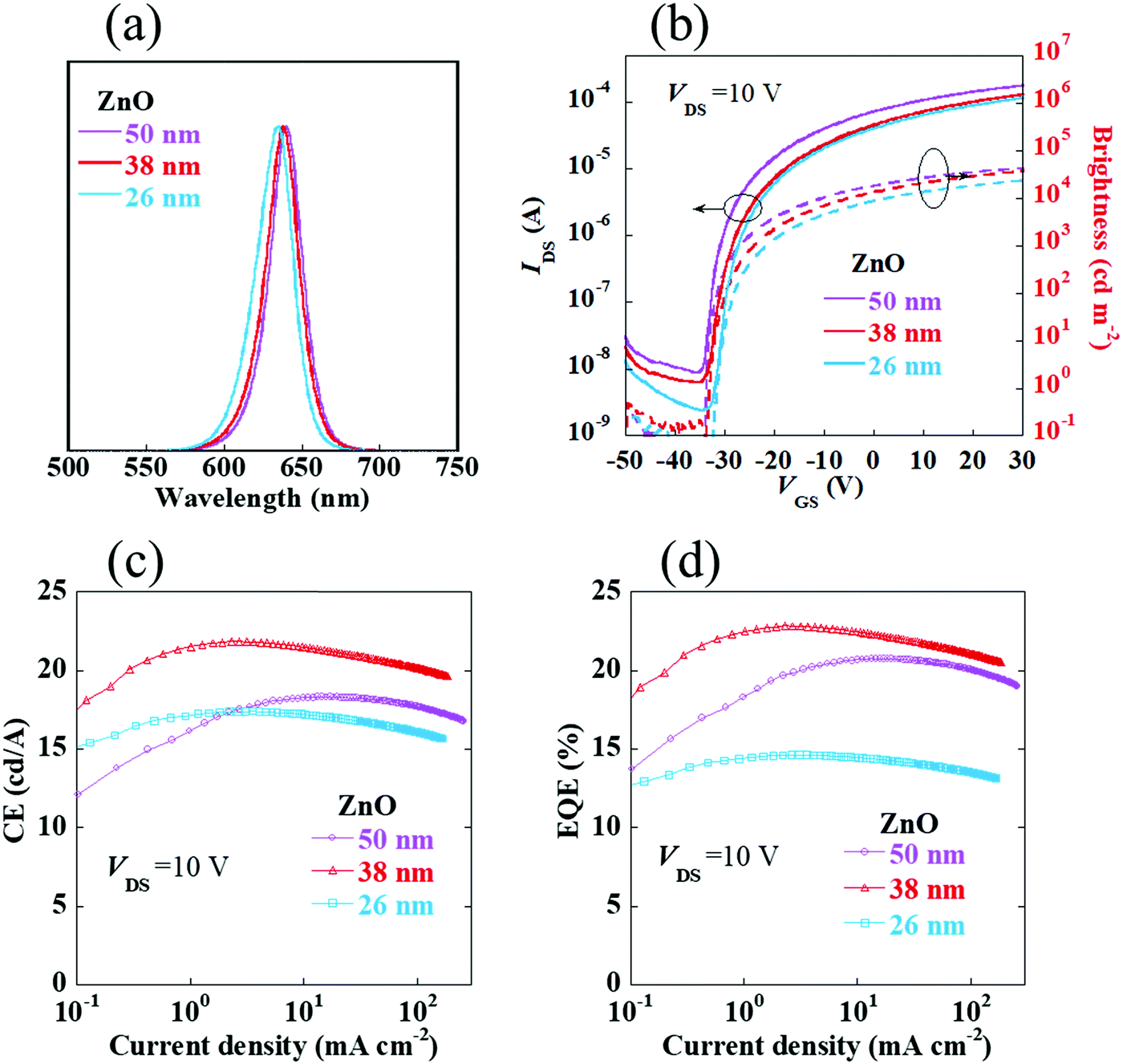 | ||
| Fig. 6 (a) The EL spectra, (b) electronic and optical transfer characteristic curves, (c) CE versus current density curves, and (d) EQE versus current density curves of red-QD-HLETs with a ZnO-nanoparticle thickness of 50 nm, 38 nm and 26 nm, respectively, measured at VDS = 10 V. | ||
Fig. 6b and c summarize the transfer curves and current efficiency curves for the red QD-HLETs with different ZnO-nanoparticle thicknesses (the detailed characteristics of the devices with 50 and 26 nm are shown in Fig. S13 and S14, respectively, ESI†). All devices exhibit typical n-type characteristics and excellent optical and electrical modulation with the gate voltage. Compared to the device with 38 nm ZnO, which has a peak EQE of 22.8%, the device with 50 nm thick ZnO-nanoparticles exhibits a peak EQE of 20.8% (with a normal peak current efficiency of 18.3 cd A−1), and the device with 26 nm thick ZnO-nanoparticles exhibits a peak EQE of 14.6% (with a normal peak current efficiency of 17.4 cd A−1). The results reveal that the efficiency of the QD-HLETs can be enhanced by adjusting the thickness of the ETLs so that the cavity resonant wavelength is close to the λPL of the QDs.
Conclusions
In summary, we have demonstrated high-performance, asymmetric solution-processed QD-HLETs, which combine the high electron mobility of the InScO/ZnO-nanoparticle heterostructure and high luminous efficiency of the core–shell QD emitting material. The QD-HLET exhibits excellent optical modulation with VGS, with a field-effect mobility of 3.1 cm2 V−1 s−1 and an on/off brightness ratio greater than 105. A brightness as high as ∼145000 cd m−2 is obtained at VGS = 30 V and VDS = 30 V. The peak CE is as high as 21.8 cd A−1, which corresponds to a peak EQE of 22.8%. The estimated operational lifetime at 100 cd m−2 is more than 153000 hours. In addition, the QD-HLET exhibits low efficiency roll-off (an EQE of 15.7% is maintained when the current density reaches as high as 1000 mA cm−2, corresponding to a brightness of ∼145000 cd m−2). To the best of our knowledge, the efficiency of the red QD-HLET is higher than those of any kinds of LETs, and even higher than those of any top-emitting QLEDs ever reported. The high performance of the QD-HLET is attributed to the following reasons.
(1) The electron/hole concentration can be well controlled by VGS and VDS, respectively, so balanced electrons and holes can be implemented by simply adjusting VGS and VDS. (2) The matched energy-level structure provides effective injection of electrons and holes. (3) The field-induced electron carriers are confined in the thin InScO semiconductor by inserting a thick ZnO-nanoparticle layer, which reduces exciton quenching induced by high electron concentration. (4) The emission is enhanced by optimizing the cavity length due to the microcavity effect.
Experimental section
Material preparation
Indium nitrate hydrate (In(NO)3·nH2O, 99.99%), scandium nitrate hydrate (Sc(NO)3·nH2O, 99.99%), 4,4′,4′′-tris(N-carbazolyl)-triphenyl-amine (TCTA) and MoOX powder were purchased from Sigma-Aldrich. Red QDs (CdSe/CdS/ZnS, diameters of 10 nm) in a colloid solution with a PLQY of the solution of 88% were purchased from Suzhou Xingshuo Nanotech Co., Ltd, and were dispersed in normal octane solution with a concentration of 20 mg ml−1. A ZnO-nanoparticle ethanol solution of 3 wt% was purchased from Pujiafu Nanotech Co., Ltd. 2.5 wt%, 2 wt% and 1.5 wt% ZnO-nanoparticle colloid solutions were prepared by mixing ethanol into 3 wt% ZnO-nanoparticle colloid solutions. The InScO precursor solutions with an In/Sc molar ratio of 92:8 were prepared by dissolving a certain amount of In(NO)3·nH2O and Sc(NO)3·nH2O in deionized water (DI) at a concentration of 0.2 M, 0.15 M and 0.1 M, respectively.
TFT fabrication
The schematic structure of the bottom-gate and top-contact TFTs is shown in Fig. 1a–c. Firstly, a aluminium–neodymium (Al:Nd, 3 wt% Nd) alloy of 300 nm thickness was deposited on glass by sputtering and patterned by wet etching for the gate electrode. Then, an anodization process was carried out to form 200 nm-thick Al2O3:Nd (38 nF cm−2) on the Al:Nd film, acting as a gate dielectric layer. The Al2O3:Nd surface was treated with ultraviolet light (UV) for 30 min to form a hydrophilic surface in the channel area defined by a stencil shadow mask. InScO films of a series of thicknesses were prepared by spin coating the InScO precursor solution with a concentration of 0.15 M at 6000 rpm for 40 s in the wettable area irradiated by UV, followed by thermal annealing in air conditions at 40 °C for 10 min and 260 °C for 1 h in sequence. A ZnO-nanoparticle colloid solution of 2.5 wt% was used to fabricate a 50 nm-thickness ZnO-nanoparticle layer by spin-coating, followed by baking at 150 °C for 15 minutes in a nitrogen glove box. After that, a top source/drain electrode of Al was deposited onto the ZnO-nanoparticle layer by thermal evaporation with a channel area of 300 μm length and 1000 μm width defined by a stencil shadow mask.QD-HLET fabrication
The schematic structure of the bottom-gate and asymmetric non-planar source/drain QD-HLETs is shown in Fig. 2a. The process for the Al:Nd gate, Al2O3:Nd gate dielectric, and InScO/ZnO-nanoparticle heterojunction is the same as that for TFTs mentioned above. ZnO-nanoparticle colloid solutions of 2.5 wt%, 2 wt% and 1.5 wt% were used to fabricate a 50-, 38- and 26 nm-thickness ZnO-nanoparticle layer, respectively. After that, the Al source electrode was deposited onto the ZnO-nanoparticle layer by thermal evaporation with a stencil shadow mask. Then, a QD emitting layer was prepared on top of the ZnO-nanoparticle layer and Al source electrode by spin-coating at 2500 rpm in a nitrogen glove box at room temperature, followed by baking at 120 °C for 10 min. 50 nm-thickness TCTA and 8 nm-thickness MoOX were deposited by thermal evaporation with a stencil shadow mask, respectively. Finally, the Au drain electrodes were deposited onto the MoOX layer by thermal evaporation using a stencil shadow mask to define a channel width/length of 500/120 μm.Device characterization
The optical and electrical characteristics of the QD-HLETs were measured using a semiconductor parameter analyzer system (Agilent B1500A) in conjunction with a probe station (Lakeshore CRX-VF) with a calibrated photodiode at room temperature under a vacuum. The normal EL spectra were obtained from an Ocean Optics QEPro fiber spectrometer integrated in the Lakeshore CRX-VF probe station. The film thickness was measured by using a surface profiler of Dektak XT and X’Pert Reflectivity. The energy levels of the functional layer were measured with an Ultroviolet Photoelectron Spectrometer (UPS) of K-ALPHA+. The absorption spectrum and transmissivity were measured by using a UV-2600. The optical microscopy images were obtained from a PTEM ZOOM 70XL with a WAT-231S2 digital camera. The brightness was calculated by comparison of the photocurrent collected from the Au drain side with that of a red QD-HLET of known brightness (measured by a KONICA MINOLTA CS-200 with a close-up lens of NO. 107) and emission area. The EQE was calculated from the brightness, the drain current, and the EL emission spectrum. The carrier mobility for the saturation regime was calculated using: | (4) |
Conflicts of interest
There are no conflicts to declare.Acknowledgements
This work was supported by the National Key R&D Program (Grant no. 2016YFB0401105), the National Natural Science Foundation of China (Grant no. 51673068), the Guangdong Province Science and Technology Plan (Grant no. 2017A050503002 and 2016B090906002), the Guangdong Natural Science Foundation (Grant no. 2017A030306007), the Guangdong Project of R&D Plan in Key Areas (Grant No. 2019B010934001 and 2020B010180001) and the Fundamental Research Funds for the Central Universities.Notes and references
- A. Hepp, H. Heil, W. Weise, M. Ahles, R. Schmechel and H. von Seggern, Phys. Rev. Lett., 2003, 91, 157406 CrossRef PubMed.
- J. Zaumseil, R. H. Friend and H. Sirringhaus, Nat. Mater., 2006, 5, 69–74 CrossRef CAS.
- R. Capelli, S. Toffanin, G. Generali, H. Usta, A. Facchetti and M. Muccini, Nat. Mater., 2010, 9, 496–503 CrossRef CAS PubMed.
- L. Hou, X. Zhang, G. F. Cotella, G. Carnicella, M. Herder, B. M. Schmidt, M. Pätzel, S. Hecht, F. Cacialli and P. Samorì, Nat. Nanotechnol., 2019, 14, 347–353 CrossRef CAS PubMed.
- S. Kahmann, A. Shulga and M. A. Loi, Adv. Funct. Mater., 2019, 30, 1904174 CrossRef.
- C. Zhang, P. Chen and W. Hu, Small, 2016, 12, 1252–1294 CrossRef CAS PubMed.
- C. Liu, X. Liu, W. Lai and W. Huang, Adv. Mater., 2018, 30, 1802466 CrossRef PubMed.
- B. B. Y. Hsu, C. Duan, E. B. Namdas, A. Gutacker, J. D. Yuen, F. Huang, Y. Cao, G. C. Bazan, I. D. W. Samuel and A. J. Heeger, Adv. Mater., 2012, 24, 1171–1175 CrossRef CAS PubMed.
- E. B. Namdas, P. Ledochowitsch, J. D. Yuen, D. Moses and A. J. Heeger, Appl. Phys. Lett., 2008, 92, 183304 CrossRef.
- M. C. Gwinner, D. Kabra, M. Roberts, T. J. K. Brenner, B. H. Wallikewitz, C. R. McNeill, R. H. Friend and H. Sirringhaus, Adv. Mater., 2012, 24, 2728–2734 CrossRef CAS PubMed.
- M. A. McCarthy, B. Liu, E. P. Donoghue, I. Kravchenko, D. Y. Kim, F. So and A. G. Rinzler, Science, 2011, 332, 570–573 CrossRef CAS PubMed.
- M. Ullah, K. Tandy, S. D. Yambem, M. Aljada, P. L. Burn, P. Meredith and E. B. Namdas, Adv. Mater., 2013, 25, 6213–6218 CrossRef CAS PubMed.
- J. Liu, I. Engquist and M. Berggren, J. Am. Chem. Soc., 2013, 135, 12224–12227 CrossRef CAS PubMed.
- X. Y. Chin, D. Cortecchia, J. Yin, A. Bruno and C. Soci, Nat. Commun., 2015, 6, 7383 CrossRef CAS PubMed.
- L. Song, Y. Hu, Z. Liu, Y. Lv, X. Guo and X. Liu, ACS Appl. Mater. Interfaces, 2016, 8, 14063–14070 CrossRef CAS PubMed.
- M. Natali, S. D. Quiroga, L. Passoni, L. Criante, E. Benvenuti, G. Bolognini, L. Favaretto, M. Melucci, M. Muccini, F. Scotognella, F. Di Fonzo and S. Toffanin, Adv. Funct. Mater., 2017, 27, 1605164 CrossRef.
- P. He, C. Jiang, L. Lan, S. Sun, Y. Li, P. Gao, P. Zhang, X. Dai, J. Wang, J. Peng and Y. Cao, ACS Nano, 2018, 12, 4624–4629 CrossRef CAS PubMed.
- K. Muhieddine, M. Ullah, B. N. Pal, P. Burn and E. B. Namdas, Adv. Mater., 2014, 26, 6410–6415 CrossRef CAS PubMed.
- X. Liu, W. Kuang, H. Ni, Z. Tao, J. Chang, Q. Liu, J. Ge, C. Li and Q. Dai, Small, 2018, 14, 1800265 CrossRef.
- K. Kajiwara, K. Terasaki, T. Yamao and S. Hotta, Adv. Funct. Mater., 2011, 21, 2854–2860 CrossRef CAS.
- K. Nomura, H. Ohta, K. Ueda, T. Kamiya, M. Hirano and H. Hosono, Science, 2003, 300, 1269–1272 CrossRef CAS PubMed.
- S. R. Thomas, P. Pattanasattayavong and T. D. Anthopoulos, Chem. Soc. Rev., 2013, 42, 6910–6923 RSC.
- E. Fortunato, P. Barquinha and R. Martins, Adv. Mater., 2012, 24, 2945–2986 CrossRef CAS PubMed.
- B. S. Mashford, M. Stevenson, Z. Popovic, C. Hamilton, Z. Zhou, C. Breen, J. Steckel, V. Bulovic, M. Bawendi, S. Coe-Sullivan and P. T. Kazlas, Nat. Photonics, 2013, 7, 407–412 CrossRef CAS.
- K. Cho, E. K. Lee, W. Joo, E. Jang, T. Kim, S. J. Lee, S. Kwon, J. Y. Han, B. Kim, B. L. Choi and J. M. Kim, Nat. Photonics, 2009, 3, 341–345 CrossRef CAS.
- X. Dai, Z. Zhang, Y. Jin, Y. Niu, H. Cao, X. Liang, L. Chen, J. Wang and X. Peng, Nature, 2014, 515, 96–99 CrossRef CAS PubMed.
- H. Shen, Q. Gao, Y. Zhang, Y. Lin, Q. Lin, Z. Li, L. Chen, Z. Zeng, X. Li, Y. Jia, S. Wang, Z. Du, L. S. Li and Z. Zhang, Nat. Photonics, 2019, 13, 192–197 CrossRef CAS.
- H. Zhang, S. Chen and X. W. Sun, ACS Nano, 2018, 12, 697–704 CrossRef CAS PubMed.
- Y. Liu, C. Jiang, C. Song, J. Wang, L. Mu, Z. He, Z. Zhong, Y. Cun, C. Mai, J. Wang, J. Peng and Y. Cao, ACS Nano, 2018, 12, 1564–1570 CrossRef CAS PubMed.
- G. Liu, X. Zhou and S. Chen, ACS Appl. Mater. Interfaces, 2016, 8, 16768–16775 CrossRef CAS PubMed.
- Z. Tang, J. Lin, L. Wang, Y. Lv, Y. Hu, Y. Fan, X. Guo, J. Zhao, Y. Wang and X. Liu, J. Mater. Chem. C, 2017, 5, 9138–9145 RSC.
- J. Song, O. Wang, H. Shen, Q. Lin, Z. Li, L. Wang, X. Zhang and L. S. Li, Adv. Funct. Mater., 2019, 1808377 CrossRef.
- J. Caruge, J. E. Halpert, V. Bulović and M. G. Bawendi, Nano Lett., 2006, 6, 2991–2994 CrossRef CAS PubMed.
- C. Murawski, K. Leo and M. C. Gather, Adv. Mater., 2013, 25, 6801–6827 CrossRef CAS PubMed.
- J. Lim, Y. Park, K. Wu, H. J. Yun and V. I. Klimov, Nano Lett., 2018, 18, 6645–6653 CrossRef CAS PubMed.
- Y. Sun, Q. Su, H. Zhang, F. Wang, S. Zhang and S. Chen, ACS Nano, 2019, 13, 11433 CrossRef CAS PubMed.
- M. U. Chaudhry, N. Wang, K. Tetzner, A. Seitkhan, Y. Miao, Y. Sun, M. C. Petty, T. D. Anthopoulos, J. Wang and D. D. C. Bradley, Adv. Electron. Mater., 2019, 1800985 CrossRef.
- J. Lee, T. Ke, J. Genoe, P. Heremans and C. Rolin, Adv. Electron. Mater., 2019, 5, 1800437 CrossRef.
- M. U. Chaudhry, K. Muhieddine, R. Wawrzinek, J. Li, S. Lo and E. B. Namdas, ACS Photonics, 2018, 5, 2137 CrossRef.
- P. E. Malinowski, T. Ke, A. Nakamura, Y. Liu, D. Vander Velpen, E. Vandenplas, N. Papadopoulos, A. J. Kronemeijer, J. van der Steen, S. Steudel, C. Kuo, Y. Huang, Y. Chen, M. Yeh, G. Gelinck and P. Heremans, J. Soc. Inf. Disp., 2018, 26, 128–136 CrossRef CAS.
- W. Cao, C. Xiang, Y. Yang, Q. Chen, L. Chen, X. Yan and L. Qian, Nat. Commun., 2018, 9, 2608 CrossRef PubMed.
- X. Hou, J. Kang, H. Qin, X. Chen, J. Ma, J. Zhou, L. Chen, L. Wang, L. Wang and X. Peng, Nat. Commun., 2019, 10, 1750 CrossRef PubMed.
- J. H. Chang, P. Park, H. Jung, B. G. Jeong, D. Hahm, G. Nagamine, J. Ko, J. Cho, L. A. Padilha, D. C. Lee, C. Lee, K. Char and W. K. Bae, ACS Nano, 2018, 12, 10231–10239 CrossRef CAS PubMed.
- Y. Park, W. K. Bae, T. Baker, J. Lim and V. I. Klimov, Nano Lett., 2015, 15, 7319–7328 CrossRef CAS PubMed.
- W. K. Bae, Y. Park, J. Lim, D. Lee, L. A. Padilha, H. McDaniel, I. Robel, C. Lee, J. M. Pietryga and V. I. Klimov, Nat. Commun., 2013, 4, 2661 CrossRef PubMed.
- T. Kamiya, K. Nomura and H. Hosono, Sci. Technol. Adv. Mater., 2010, 11, 044305 CrossRef PubMed.
Footnote |
| † Electronic supplementary information (ESI) available. See DOI: 10.1039/d0mh00951b |
| This journal is © The Royal Society of Chemistry 2020 |