Single-step synthesis and magnetic separation of graphene and carbon nanotubes in arc discharge plasmas†
O.
Volotskova
a,
I.
Levchenko
bc,
A.
Shashurin
a,
Y.
Raitses
d,
K.
Ostrikov
*bc and
M.
Keidar
*a
aDepartment of Mechanical and Aerospace Engineering, The George Washington University, Washington, DC 20052, USA. E-mail: keidar@gwu.edu
bPlasma Nanoscience Centre Australia (PNCA), CSIRO Materials Science and Engineering, P.O. Box 218, Lindfield, NSW 2070, Australia. E-mail: Kostya.Ostrikov@csiro.au
cPlasma Nanoscience, School of Physics, The University of Sydney, Sydney, NSW 2006, Australia
dPrinceton Plasma Physics Laboratory, Princeton, New Jersey 08543, USA
First published on 16th August 2010
Abstract
The unique properties of graphene and carbon nanotubes made them the most promising nanomaterials attracting enormous attention, due to the prospects for applications in various nanodevices, from nanoelectronics to sensors and energy conversion devices. Here we report on a novel deterministic, single-step approach to simultaneous production and magnetic separation of graphene flakes and carbon nanotubes in an arc discharge by splitting the high-temperature growth and low-temperature separation zones using a non-uniform magnetic field and tailor-designed catalyst alloy, and depositing nanotubes and graphene in different areas. Our results are very relevant to the development of commercially-viable, single-step production of bulk amounts of high-quality graphene.
Introduction
Graphene flakes (GFs) and carbon nanotubes (CNTs) are very promising for molecular sensors, single-electron transistors, supercapacitors, non-volatile memory devices, integrated circuits, atomic-scale switches and other carbon-based electronic and magneto-electronic devices.1–4 GFs and CNTs also demonstrate unique mechanical properties, thus being the most prominent candidates for micro- and nano-electromechanical systems.5–7 The production of GFs and CNTs usually requires very specific and non-equilibrium process conditions, namely a high influx of carbon material to the developing structures, relatively high temperatures, as well as the presence of a custom-designed catalyst. That is why the nanotubes were first discovered in carbon deposits of the arc discharge, where the above non-equilibrium conditions can be easily maintained owing to the effect of high-density plasmas.8–10 Now, the arc discharge technique ensures the nanotube production in bulk amounts,11 and remains among the most advanced and versatile techniques suitable for large-scale production of high-quality carbon nanotubes. Most recently, arc discharge plasmas have also been successfully used for the synthesis of graphene flakes.12,13 However, the issues of the GF large-scale production and process control still remain essentially unresolved. Indeed, the majority of the surface-based methods, such as micro-mechanical exfoliation,14 epitaxial growth on electrically insulating surfaces15 and graphene formation by thermal decomposition or thermal annealing of silicon carbide16 and others17 have not reached the expected process yields. This is why the arc discharge-based technique still remains the most promising method for synthesizing high-quality GFs at industrial scales.Given the phenomenal success of arc discharges in the synthesis of high-quality CNTs in large amounts, and taking into account the structural similarities of the GFs and the CNTs, further development of the arc discharge-based systems for the effective, high-throughput techniques for large-scale production of freestanding graphene and carbon nanotubes is a highly demanding issue. Moreover, since the CNTs and the GFs are in most cases produced simultaneously, in the same discharge, the development of the most commercially-viable, single-step processes would require the discovery of the effective means of the effective separation of these two nanostructures after the growth process is complete. However, it is still not known how to separate the graphene from nanotubes that are produced simultaneously in this very fast process.18,19
In this paper, we report on a novel, single-step approach to simultaneous production and separation of graphene flakes and carbon nanotubes in the arc discharge plasmas. We demonstrate that high quality graphene flakes and carbon nanotubes can be effectively synthesized in the magnetic field – enhanced arc discharge, and then deposited in different areas of the discharge enhancing/separating magnet unit. The carbon samples were analysed with the SEM, TEM, AFM, and Micro Raman techniques.
Results and discussion
General approach
We have approached this problem deterministically, noting that the effective production and separation of high-quality GFs and CNTs in a single-step process set quite conflicting requirements. Indeed, during the growth, both the GF and the CNTs should be kept in the same discharge zone with the optimum nucleation and growth conditions. Specifically, our approach relies on the unprecedented combination of high-density plasma arc discharge with the unique ability to produce simultaneously the high-quality carbon nanotubes and graphene flakes. A customized non-uniform magnetic field is used to split the simultaneous production of high-quality carbon nanotubes and graphene flakes in the high-temperature, high-plasma-density growth zone of the arc discharge, and magnetic separation of the nanotubes and graphene in the low-temperature, low-plasma-density separation zone of the arc discharge whereupon the tailor-designed Y-Ni catalyst transits from a non-magnetic and nanostructure growth-supporting state in the hot growth zone to a ferromagnetic and growth-inhibiting state in the cold separation zone. After that, mass-dependent magnetic separation force leads to very effective deposition of the nanotubes and graphene in very different collection areas.Graphene and nanotube production and separation
With an external magnetic field applied to the discharge, the plasma temperature and density significantly increase. The plasma density is increased due to the effect of the magnetic field which focuses the plasma jet. Indeed, magnetic confinement restricts the plasma boundaries and prevents the plasma from expansion. Another reason is the magnetization of plasma electrons which leads to more effective ionization of the neutral gas atoms by electron impact. The plasma temperature, in turn, increases in the magnetic field due to the stronger electric field in the magnetized plasma, in contrast to the non-magnetic conditions.20,21In dense plasmas, the ion bombardment associated processes (mainly sputtering and heating) can play a significant role in the nucleation and growth of graphene. Along with this, the electron temperature in arc discharge plasmas is not too high. Hence, the floating potential of the nanostructures in the plasma does not exceed several volts. As a result, the energy of ions bombarding the carbon nanostructure is low, so is the sputtering rate. This is why the ion-related heating is the most important effect. Besides, the rate of carbon deposition to nanostructures is also enhanced by the influx of neutral atoms whose thermal energy is too low for any effective sputtering.22
In the growth zone, the ambient temperature is much higher than the Curie point of the catalyst nanoparticles which therefore remain hot and non-magnetic. This is why the growth conditions are determined by the high catalyst temperature and also a strong incoming flux of carbon material. Outside of the optimum growth zone, the plasma temperature and hence the catalyst temperature decrease sharply. Further away, the temperature decreases below the Curie point, the catalyst particles become ferromagnetic, respond to the magnetic field, and the separation process starts. Thus, the boundary between the growth and the magnetic separation zones is determined by the catalyst alloy and the plasma parameters. Indeed, in the high-density plasma the catalyst is hot and non-magnetic; both GF and CNT are developing in the optimum growth zone with no magnetic separation.
On the other hand, in the separation zone the plasma density and the temperature are low, and the catalyst is cold. Hence, while the growth is disabled, the magnetic separation starts. To this end, the optimized composition of the two transition metals, yttrium (which is paramagnetic) and nickel (ferromagnetic with the Curie temperature of about 350 °C) was used. Nickel exhibits very high carbon solubility but does not form carbon-containing compounds without oxygen, thus ensuring an efficient carbon supply to the nanostructures.23 On the other hand, yttrium easily forms carbides, and as such enables a very quick nucleation of the carbon nanostructures. Note that the melting points for both these metals are very close, so the catalyst alloy nanoparticles have a stable aggregate structure. In this way, the Y-Ni catalyst alloy was customized to exhibit the excellent nucleation/growth support ability when hot (in the optimum growth zone), and the ferromagnetic response when cooled down below 350 °C (in the magnetic separation zone). Our previous experiments have proven the effectiveness of this catalyst alloy for the large-scale carbon nanostructure production.24
Characterization of graphene samples
The carbon samples were collected from the discharge enhancing/separating magnet unit (DESMU) side and top surfaces, and from the chamber walls; detailed description of the experimental setup can be found in the ESI.†Fig. 1 shows the images of the representative structures produced. The nanostructured carbon (graphene flakes) could be found on the magnet surfaces, whereas lacey carbon was found on the chamber walls. The carbon samples were collected and then analyzed with the SEM, TEM, AFM, and micro Raman techniques. In Fig. 2 we show representative SEM and TEM images of carbon samples collected from various parts of the setup. Fig. 2a, 2b, and 2c are the low-, medium-, and high-magnification SEM images, respectively, of the samples containing graphene layers, collected from the top and side surfaces of the magnet (see Fig. 1). The estimated size of the graphene flakes is approximately 500–2500 nm, with up to 10 graphitic layers. Some graphene flakes show explicit crystallographic faceting (e.g., clearly visible hexagon sections in Fig. 2c). It is also seen that the graphene flakes are surrounded and partially covered by loose carbon. Fig. 2d and 2e show TEM images of folded graphene layers in the carbon samples collected from the top and side surfaces of the magnet, respectively. It is seen that these fragments contain a few flake-like graphene layers, up to 3. In Fig. 2f we show the TEM image of the sample containing carbon nanotubes, collected from the side surfaces (remote from the discharge) of the DESMU. It should also be pointed out that a typical catalyst size found by the TEM was approximately 2 to 10 nm. The SEM analysis of the deposits found on the magnet allows a rough estimate of the production rate to be about 1 cm2 of graphene per hour of operation of the arc discharge at 50 A, or 0.02 cm2 h−1A−1.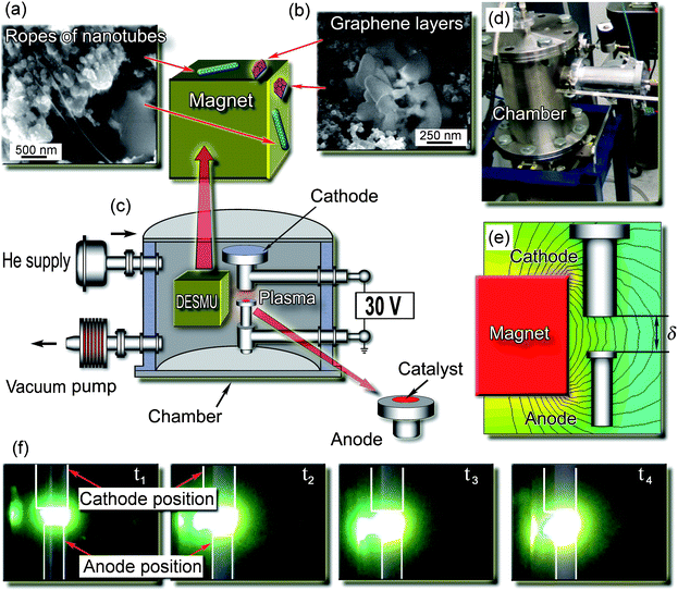 | ||
| Fig. 1 Experimental setup, photo of the plasma reactor and discharge, and SEM micrographs of representative graphene flakes. (a, b) Representative SEM images of the carbon deposit collected from different collection areas. Ropes of carbon nanotubes found on the top and side surfaces of the DESMU, in the areas close to the discharge; graphene layers found on the top and side surfaces of the DESMU, in the areas remote from the discharge. An effective separation of the two different carbon nanostructures was ensured. (c) Schematic of the experimental setup. (d) Photograph of the experimental setup. (e) Schematic of the mutual position of the cube-shaped magnet, anode and cathode, and the computed 2D map of the magnetic field (field strength of 1.2 kG in the discharge gap was optimized for the highest yield of both GFs and CNTs). (f) Consecutive photographs of the discharge development in the non-uniform magnetic field. | ||
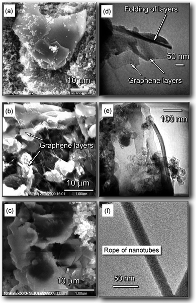 | ||
| Fig. 2 Representative SEM and TEM images of various carbon deposits collected in different collection areas. (a–c) Low-, medium-, and high-magnification SEM images of the samples containing graphene layers, collected from the top and side surfaces of the magnet. (d, e) TEM image of folded graphene layers in the carbon sample collected from the top and side surfaces of the magnet, respectively. (f) TEM image of the sample containing carbon nanotube bundles, collected from the side surfaces (remote from the discharge) of the magnet. | ||
In Fig. 3 we show the results of characterization of the samples collected at the top surface of the DESMU by the AFM, Raman, and selected area electron diffraction (SAED) techniques. The atomic force microscopy clearly revealed the presence of flake-like structures with the surface size of around one micron and a height variation of 1.5 nm (Fig. 3a, b). The Raman characterization of the specimens collected from the side surfaces of the magnet showed the occurrence of a weak D-peak at around 1325 cm−1, which is related to the amount of defects in sp2 bonds (Fig. 3c).25 The SAED TEM pattern from a similar specimen collected from the top surface of the magnet is shown in Fig. 3e. It reveals the pattern expected for a hexagonal close-packed crystal with the incident beam close to (0001) plane; some additional details on the results obtained by the Raman spectroscopy can be found in the ESI.†
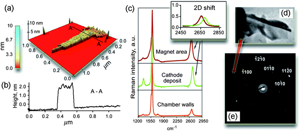 | ||
| Fig. 3 Microanalysis of the samples shown in Fig. 1 and 2. (a, b) 3D reconstruction and profile of the specimens collected at the top side of the magnet. The presence of flake-like structures with the surface size of around 1 μm2 and a height variation of 1–2 nm, as well as the occurrence of “bumps/wrinkles” with the height variation about ∼0.5 nm are clearly revealed. (c) Raman spectra of the samples collected from the side surfaces of the magnet, cathode, and chamber walls. (d) Fragment of TEM photo of the folded graphene layers. (e) SAED pattern generated by the specimen collected from the top surface of the magnet. | ||
Experimental
The GFs and CNTs were produced in an arc discharge setup fitted with an additional discharge enhancing/separating magnet unit (DESMU), a graphite cathode of 0.5 in. dia., and a graphite hollow rod anode of 0.25 in. dia. filled with a mixture of carbon and Y-Ni catalyst powder (particle size of 0.1 to 1 mm) in 1![[thin space (1/6-em)]](https://www.rsc.org/images/entities/char_2009.gif) :4 ratio. The process was conducted in a cylindrical stainless steel chamber with the total volume of 4500 cm3 (27 cm in length and 14.5 cm dia.). The graphite anode and cathode were oriented along the vertical axis of the chamber. Graphene and nanotube samples were collected from the top and side surfaces of the DESMU (permanent magnet sides), the total collection area was 2500 mm2. The permanent magnet installed in the DESMU was not externally biased, i.e., it was under the floating potential. With the typical electron temperature in the discharge plasma being 0.5–1.0 eV,20 the floating potential of the magnet (and hence the potential of the sample collection surfaces) was only several volts. Our previous experiments have demonstrated that helium discharges are very effective for the carbon nanostructure production.21,26,27 This is why the process was conducted in helium at a gas pressure of 500 Torr. The graphene collection surfaces were cleaned from the deposit after each experiment and degreased with methanol before running the process. The detailed description of the system can be found in the ESI,† and also in our recent publications.21,24
:4 ratio. The process was conducted in a cylindrical stainless steel chamber with the total volume of 4500 cm3 (27 cm in length and 14.5 cm dia.). The graphite anode and cathode were oriented along the vertical axis of the chamber. Graphene and nanotube samples were collected from the top and side surfaces of the DESMU (permanent magnet sides), the total collection area was 2500 mm2. The permanent magnet installed in the DESMU was not externally biased, i.e., it was under the floating potential. With the typical electron temperature in the discharge plasma being 0.5–1.0 eV,20 the floating potential of the magnet (and hence the potential of the sample collection surfaces) was only several volts. Our previous experiments have demonstrated that helium discharges are very effective for the carbon nanostructure production.21,26,27 This is why the process was conducted in helium at a gas pressure of 500 Torr. The graphene collection surfaces were cleaned from the deposit after each experiment and degreased with methanol before running the process. The detailed description of the system can be found in the ESI,† and also in our recent publications.21,24
We have found that the magnetic field strongly enhances the arc discharge. Indeed, with the DESMU installed, the plasma arc (normally confined between the cathode and the anode) is stretched towards the magnet. Several consecutive photographs for the four time moments are shown in Fig. 1 from which one can see that the arc discharge is indeed altered by the external non-uniform magnetic field and becomes anisotropic, due to strong magnetization of the plasma electrons in the magnetic field as can be seen in Fig. 1. The test runs without the use of the catalyst, as well as the similarly catalyzed process conducted at zero magnetic field did not reveal any significant nanostructure growth.
Conclusions
Our unique, yet simple plasma-enabled approach demonstrates a novel deterministic technique for the effective large-scale, single-step synthesis and separation of the high-quality carbon nanotubes and graphene flakes in arc discharge plasmas. This in turn offers tantalizing prospects for the numerous applications in molecular sensors, single-electron transistors, supercapacitors, non-volatile memory devices, integrated circuits, atomic-scale switches and other carbon-based electronic and magneto-electronic devices.Acknowledgements
This work was supported in part by NSF STTR program (NSF grant IIP-1010133) and NSF/DOE Partnership in Plasma Science and Technology (NSF grant CBET-0853777, DOE grant DE-SC0001169). We would like to acknowledge PPPL Offsite Research Program supported by Office of Fusion Energy Sciences for supporting arc experiments. Authors thank Jon Torrey for help with AFM and Jian Li for help with TEM. Authors thank Jeffrey Fagan and Frederick R. Phelan for stimulating discussions. This work was partially supported by CSIRO and Australian Research Council.References
- C. Rutherglen, D. Jain and P. Burke, Nat. Nanotechnol., 2009, 4, 811 CrossRef CAS.
- F. Li, Y. Huang, Q. Yang, Z. Zhong, D. Li, L. Wang, S. Song and C. Fan, Nanoscale, 2010, 2, 1021 RSC.
- Z. Dong, P. Kashkarov and H. Zhang, Nanoscale, 2010, 2, 524 RSC.
- A. Kaniyoor, R. I. Jafri, T. Arockiadoss and S. Ramaprabhu, Nanoscale, 2009, 1, 382 RSC.
- R. M. Sankaran and W.-H. Chiang, Nat. Mater., 2009, 8, 882 CrossRef.
- G. Tsoukleri, J. Parthenios, K. Papagelis, R. Jalil, A. C. Ferrari, A. K. Geim, K. S. Novoselov and C. Galiotis, Small, 2009, 5, 2397 CrossRef CAS.
- P. M. Ajayan and J. M. Tour, Nature, 2007, 447, 1066 CrossRef CAS.
- M. Mozetic, U. Cvelbar, M. K. Sunkara and S. Vaddiraju, Adv. Mater., 2005, 17, 2138 CrossRef CAS.
- J. Shieh, H. L. Chen, T. S. Ko, H. C. Cheng and T. C. Chu, Adv. Mater., 2004, 16, 1121 CrossRef CAS.
- U. Cvelbar, Z. Chen, M. K. Sunkara and M. Mozetic, Small, 2008, 4, 1610 CrossRef CAS.
- S. Iijima, Nature, 1991, 354, 56 CrossRef CAS.
- S. Karmakar, N. V. Kulkarni, A. B. Nawale, N. P. Lalla, R. Mishra, V. G. Sathe, S. V. Bhoraskar and A. K. Das, J. Phys. D: Appl. Phys., 2009, 42, 115201 CrossRef.
- K. S. Subrahmanyam, L. S. Panchakarla, A. Govindaraj and C. N. R. Rao, J. Phys. Chem. C, 2009, 113, 4257 CrossRef CAS.
- K. S. Novoselov, D. Jiang, F. Schedin, T. J. Booth, V. V. Khotkevich, S. V. Morozov and A. K. Geim, Proc. Natl. Acad. Sci. U. S. A., 2005, 102, 10451 CrossRef CAS.
- E. V. Rut'kov and A. Y. Tontegode, Surf. Sci., 1985, 161, 373 CrossRef CAS.
- T. Ohta, F. Gabaly, A. Bostwick, J. L. McChesney, K. V. Emtsev, A. K. Schmid, T. Seyller, K. Horn and E. Rotenberg, New J. Phys., 2008, 10, 023034 CrossRef.
- W. Chen and L. Yan, Nanoscale, 2010, 2, 559 RSC.
- G. Eda and M. Chhowalla, Adv. Mater., 2010, 22, 2392 CrossRef CAS.
- S. Arepalli, J. Nanosci. Nanotechnol., 2004, 4, 317 CrossRef CAS.
- I. I. Beilis, M. Keidar, R. L. Boxman and S. Goldsmith, Phys. Plasmas, 2000, 7, 3068 CrossRef CAS.
- M. Keidar, I. Levchenko, T. Arbel, M. Alexander, A. M. Waas and K. Ostrikov, J. Appl. Phys., 2008, 103, 094318 CrossRef.
- I. Levchenko, K. Ostrikov and M. Keidar, J. Nanosci. Nanotechnol., 2008, 8, 6112 CrossRef CAS.
- A. Moisala, A. G. Nasibulin and E. I. Kauppinen, J. Phys.: Condens. Matter, 2003, 15, S3011 CrossRef CAS.
- M. Keidar, I. Levchenko, T. Arbel, M. Alexander, A. M. Waas and K. Ostrikov, Appl. Phys. Lett., 2008, 92, 043129 CrossRef.
- C. Thomsen and S. Reich, Phys. Rev. Lett., 2000, 85, 5214 CrossRef CAS.
- M. Keidar, A. M. Waas, Y. Raitses and E. Waldorff, J. Nanosci. Nanotechnol., 2006, 6, 1309 CrossRef CAS.
- I. Levchenko, D. Mariotti and K. Ostrikov, Carbon, 2009, 47, 344 CrossRef CAS.
Footnote |
| † Electronic supplementary information (ESI) available: Details of the setup and process; details on the micro-Raman, TEM, SEM, AFM, and characterization of the carbon deposits in different collection areas; detailed description of the results obtained by micro-Raman, AFM and electron diffraction techniques. See DOI: 10.1039/c0nr00416b |
| This journal is © The Royal Society of Chemistry 2010 |