Insights into the capping and structure of MoS2 nanotubes as revealed by aberration-corrected STEM†
Francis Leonard
Deepak
ab,
Alvaro
Mayoral
a,
Andrew J.
Steveson
a,
Sergio
Mejía-Rosales
ac,
Douglas A.
Blom
d and
Miguel
José-Yacamán
*a
aDepartment of Physics and Astronomy, University of Texas at San Antonio, One UTSA Circle, San Antonio, TX 78249, USA. E-mail: miguel.yacaman@utsa.edu; Fax: (+210) 458-4919; Tel: (+210) 458-5451
bInternational Iberian Nanotechnology Laboratory, Avda Mestre Jose Veiga, Braga 4715, Portugal
cCenter for Innovation and Research in Engineering and Technology and Facultad de Ciencias Físico-Matemáticas, Universidad Autónoma de Nuevo León, San Nicolás de los Garza, NL 66450, México
dEM Center, University of South Carolina, 715 Sumter St, Coker Life Sciences 001, Columbia, SC 29208, USA
First published on 18th August 2010
Abstract
Aberration-corrected electron microscopy (STEM-HAADF) has been used for the first time to understand the capping, nature and structure of the MoS2 nanotubes. The MoS2 nanotubes that have been obtained have various unusual faceted caps presumably arising from the presence of topological defects. A detailed study of the capping of the nanotubes, along with identification that the MoS2 nanotubes are of the zigzag type have been carried out using both experimental and simulated STEM images. The presence of 3R-rhombohedral stacking of the MoS2 nanotubes has been identified.
1. Introduction
Capped nanotubes including those of carbon have generated great interest, mainly because of their properties as field-emission (FE) sources.1 In the case of capped carbon nanotubes (CNTs), the closed apex with each carbon atom is bound to three neighboring atoms via covalent bonds, thereby its much higher FE stability than that of an opened end. Thus, capped CNTs have become the focus of scientific and industrial interest for their potential uses as, for example, high-brightness point-electron sources. In order to achieve this, controlled removal of carbon atoms at the tip of the CNT was realized and various tip structures were fabricated and the corresponding FE was measured, showing thereby, the superior field-emission characteristics.2 Nanotube caps can have various structures, shapes and degrees of curvature: nanotubes can be capped by fullerene hemispheres, but caps can also have different levels of sphericity and arrangements of atoms, and can also be nearly flat, conical or bill-like.3 The only absolute requirement is that they satisfy Euler's theorem, which states that in order to achieve complete closure of a hexagonal lattice of any size or shape, it is necessary to incorporate a total of exactly twelve pentagons. In the case of nanotubes with uniform circular or elliptical cross-sections along the axis each capping side must include atleast six pentagons although this may vary with the different nanotubes. Subsequent to the discovery of CNTs, conical tips were observed by Iijima et al.4 In the case of the nanotubes with the conical shape the number of pentagons at the ends may be different. Thus in the case of conical caps observed by Iijima et al. these were proposed to have five pentagons according to Euler's theorem. CNTs were demonstrated to be suitable tips for SPM and thereafter the utility of hemispherically capped single-wall carbon nanotubes for use as scanning force microscope tips was investigated using molecular dynamics.5,6Apart from carbon nanotubes, inorganic nanotubes, especially those of BN and transition metal chalcogenides like WS2 could also form interesting capped nanotubes.7–9 Hexagonal boron nitride (h-BN) is layered material with a graphite-like structure, in which planar networks of BN hexagons are stacked regularly. Nanotubes of boron nitride synthesized by various methods have shown interesting morphologies exhibiting a flat tip, bulbous, club-like, as well as “triangular flag” like shapes at their tips. These kind of morphologies suggests the presence of energetically unfavorable odd-membered rings (e.g., pentagons and heptagons) in addition to favorable even membered rings (e.g., squares).10–13 A flat tip with right-angle corners is the most common morphology for hexagonal BN networks. The right angle termination results from the presence of four-membered rings (B2N2 squares) at the tip, instead of five-membered rings. Even-numbered rings (e.g., squares, hexagons, and octagons) preserve energetically favorable B–N bonds, while odd-numbered rings (e.g., pentagons) introduce unfavorable B–B (or N–N) bonds. In the case of the “triangular flag” like shape, the formation of such a tip can be realized by placing two squares (four-membered rings) at the acute corners and one heptagon at the base of the triangular flag. One square introduces a +2ð/3 disclination in the hexagonal BN network, while one heptagon introduces a −ð/3 disclination. Thus a set of disclinations with angles adding up to 2ð is required to close one end of a tube.
Transition metal chalcogenides like MoS2 or WS2 are quasi-two dimensional (2D) compounds. Atoms within a layer are bound by strong covalent forces, while individual layers are held together by van der Waals (vdW) interactions. Although there are a large number of polytypes observed in the case of the transition metal chalcogenides the most notable experimentally observed polytypes in the case of MoS2 and WS2 based on the stacking sequence of the layers are either a hexagonal polymorph with two layers in the unit cell- 2H (P63/mmc) symmetry, rhombohedral with three molecular layers in the unit cell layers—3R (R3m) symmetry and the less common trigonal with one layer—1T.7 Similar to carbon, transitional metal chalcogenides also form close caged structures known as inorganic fullerenes (IF) and nanotubes (INTs).7–9 As far as capping in the case of transition metal chalcogenide nanotubes are concerned, WS2 nanotubes synthesized by reacting WOx nanorods with H2S revealed various cap formations. A detailed molecular mechanics computer simulation was used to establish two types of IF nanotube cap, i.e., by introducing square-like and octagonal-like defects associated with zigzag and armchair nanotubes, respectively.14 Both these two types of defective structure could equally well be formed, thus leading to either zigzag or armchair tubes.14 Similar to the carbon nanotubes, the rolling up of the sheets of MoS2 along selected directions can lead to the formation of the tubular structure of MoS2. This may be described in terms of the primitive 2D lattice vectors ![[a with combining right harpoon above (vector)]](https://www.rsc.org/images/entities/i_char_0061_20d1.gif) and
and ![[b with combining right harpoon above (vector)]](https://www.rsc.org/images/entities/i_char_0062_20d1.gif) are two integer indices:
are two integer indices: ![[B with combining right harpoon above (vector)]](https://www.rsc.org/images/entities/i_char_0042_20d1.gif) = n + m . In this way three classes of nanotubes can be distinguished: n = m (“armchair” nanotubes), – n ≠ 0, m = 0 (“zigzag” nanotubes), – and n ≠ m (“chiral nanotubes”).
= n + m . In this way three classes of nanotubes can be distinguished: n = m (“armchair” nanotubes), – n ≠ 0, m = 0 (“zigzag” nanotubes), – and n ≠ m (“chiral nanotubes”).
Insights into the type and structure of nanotubes and the formation of nanotube caps were limited before the advent of aberration-corrected microscopes. Subsequent to the introduction of such microscopes there have been substantial progress in this direction. Aberration-corrected electron microscopy for the study of inorganic nanotubes, especially those of the transition metal chalcogenides (ex: WS2) is a very recent area of exploration.15,16 The elucidation of structure and chirality is essential to the understanding of how nanotubes can have suitable electronic, mechanical and other related properties. This thereby can help the preferential and improved synthesis of nanotubes suited for specific applications. Investigations on nanotubes using aberration-corrected microscopy along with theoretical calculations will enable a hand-in-hand progress of the field that at present is the most immediate requirement. We have sought to use probe aberration-corrected electron microscopy for elucidating some important features and aspects of MoS2 nanotubes. Thus we have synthesized MoS2 nanotubes, and during the course of the analysis we have observed some important features, namely, faceted caps in these nanotubes as well as unusual stacking of the Mo–S in the layers that make up the nanotubes. It must be pointed out here that there is a sandwich layer of atoms in every layer (for example S–Mo–S) that make up the individual layers of the nanotube and the way these coordinate amongst themselves lead to the unusual capping of MoS2 nanotubes which is very different from that of carbon. Aberration-corrected electron microscopy along with simulated STEM images has been carried out to understand better the structure of the nanotubes. Further details involving the nature of the nanotubes, as well as the structure and bonding of the Mo–S in the nanotubes have been investigated, and our results have revealed various interesting aspects for the first time to our knowledge. We hope that such a study will enable great interest and subsequent investigations on unraveling some of the hitherto unknown facts about nanotubes in the light of new advanced microscopic techniques.
2. Experimental section
2.1 Synthesis
The synthesis of the MoS2 Nanotubes involved a two-step process: In the first step MoO3 nanobelts were synthesized by a simple hydrothermal procedure, and subsequently in the second step it was followed by the sulfidization of the as-synthesized MoO3 nanobelts into MoS2 nanotubes using a H2S/H2 gas mixture. 100 mg of MoO3 nanobelts was placed in a ceramic boat. The ceramic boat was centered inside a quartz tube, placed inside a tube furnace and heated to 900 °C in flowing N2. When the desired temperature was reached a mixture of H2/H2S (1% H2 and 99% H2S or 10% H2 and 90% H2S) was turned on and the N2 flow turned off. The reaction in the presence of flowing H2/H2S mixtures was carried out for 30 min. After the reaction, the N2 flow was reactivated and the H2/H2S gas mixture was turned off and the reaction was shut down and allowed to cool. After the reaction the grey colored sample collected from the boat was used for further analysis (see supplementary information†).2.2 Characterization
For the electron microscopy analysis, the grey coloured powder was dispersed in ethanol and a drop of this suspension was deposited onto a holey carbon microgrid. The MoS2 nanotubes were characterized using a Hitachi S-5500 scanning electron microscope (SEM) with a bright-field/dark-field duo STEM detector. A JEOL 2100F field-emission gun transmission electron microscope (FEG-TEM) operating at 200 kV (point resolution of 0.19 nm) and a JEOL JEM-2010F (FEG-TEM) operated at 200 kV with a 0.1 nm lattice resolution were employed to record high resolution (HRTEM) images, electron diffraction (ED) patterns and to perform the EDX analysis of the materials. For the aberration-corrected (Cs corrected) characterization, the samples were analyzed using Scanning transmission electron microscopy (STEM) with a JEOL 2100F, 200 kV FEG-STEM/TEM equipped with a CEOS Cs corrector on the illumination system. The geometrical aberrations were measured and controlled to provide less than a π/4 phase shift of the incoming electron wave over the probe-defining aperture of 15.5 mrad. High-angle annular dark-field (HAADF) STEM images were acquired using a Fischione Model 3000 HAADF detector with a camera length such that the inner cut-off angle of the detector was 50 mrad. STEM images were recorded for 16 to 20 s. In order to reduce the noise of the images and to obtain clearer images the raw data was filtered using the Richardson–Lucy algorithm implemented by Ishizuka.17a The simulated STEM images were generated using the xHREM program.17b The simulated STEM images were generated at 200kV, with a Cs aberration of 0.01mm, and a dark field detector range of 50–100 mrad. To analyze the way the nanotubes close themselves at their ends, we applied geometrical phase analysis (GPA) to several micrographs, using the GPA for DigitalMicrograph tool developed by HREM Research.17,18 With this analysis which is based on the mapping of the phase shift of the lattice represented in the micrograph, it is possible to measure distortions of the molecular arrangement, and, if resolution is high enough, to compute strain components.3. Results and discussion
Fig. 1 shows several MoS2 nanotubes capped in different ways. Marked by the white arrow in the figure is a 90° wall-cap junction, and the conical capped structure at the tip of the nanotubes is marked by the black arrow. There seem to be two different kinds of conical capping, as can be seen from the figure. A closer look at the different conical capped structures is shown in Fig. 2a–d. There appears to be a considerable amount of strain associated with obtaining such sharp conical tips as revealed by the formation of discontinuous layers around the tip of the nanotube, as can be seen in the figures (marked by the black arrows). In all of these nanotubes the layers that make up these kinds of caps seems to be discontinuous, probably due to the strain associated with their formation. The outer layer of the disulfide nanotubes and the inorganic fullerenes are almost always complete, but the inner layers show defects, dislocations, and terminated growth.8 This results in differences in the wall thickness on the two sides and in the varying diameter of the inner core along the length of the tube wall. This type of terminated growth has not been reported in hollow CNTs, but it has been found in metal-filled CNTs.19 The terminated layer may be a manifestation of the defective structure of the starting precursor, or can be due to the absence of growing material at the edges. Layer defects have been observed previously in WS2 nanotubes. These defects can be traced back to the crystallographic shear in the starting precursor phase.20 Rémskar et al. showed that each WS2 layer has to satisfy the stacking order and orientation relationship with respect to the previous layer and the strain involved can be relaxed by the formation of edge dislocations.21 The outer cylinders are subjected to less stress than the inner cylinders, and this internal stress stabilizes the inner shells, while the outer layers become easy to deform resulting in a greater number of defects near the edges and thus forming such interesting capped structures. The last variation in the capped end of the nanotube is shown in Fig. 3, where clear and distinct facets form the cap. The capping structure is reminiscent of the cutting of an octagon into half sections in order to cap the end of the nanotube. To obtain nanotubes with capping is quite unusual.22 From our experience and from reports in literature, MoS2 nanotubes have been predominantly obtained with open ends.23–26 Intrigued by the prospect of obtaining such nanotubes with unusual closed ends we sought to investigate the capping of these nanotubes obtained in the present synthesis and indeed we found out that there were many interesting features worth to discuss.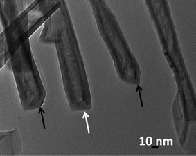 | ||
| Fig. 1 TEM images of the MoS2 nanotubes with various unusual caps. Shown in white arrow in the image is the flat cap, whereas the black arrow in the image shows the conical caps. | ||
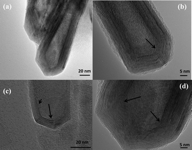 | ||
| Fig. 2 (a) MoS2 nanotubes with conical caps, (b)–(d) various modifications of the conical capping. The black arrows in the images reveal the strain involved and the discontinous layers that make up the tips of the nanotube. | ||
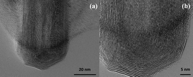 | ||
| Fig. 3 (a) HRTEM image and (b) a close up-view of the MoS2 nanotubes which reveal a half-octagonal capped structure making the cap of the nanotube. | ||
Fig. 4 shows the STEM images of the MoS2 nanotubes with varied capped features recorded from the probe aberration-corrected microscope which was used in this study. Fig. 4a shows the STEM image of a MoS2 nanotube with a conical cap. A closer look at the nanotube layers is shown in Fig. 4d (marked by the white box in Fig. 4a). The bright spots revealed in the micrograph are due to the presence of Mo atoms that can be clearly seen in the image. The distance between the Mo–Mo atoms in a single layer is found to be ∼2.8 Å. This is in accordance with the observed distances between the atoms of Molybdenum.27,28 Significantly the Mo–Mo interatomic distance in the case of the as-obtained MoS2nanotubes has been measured in the present study and is exclusive to the present report. Previously the measured Mo–Mo distances have been in the case of the nanoseashells and nanooctahedra of MoS2.27,28 The interlayer spacing measured is close to 0.63 nm in the case of the layers of the MoS2 nanotubes (in the region marked as A). However closer to the ends of the nanotube, where the formation of the conical tips is located, the interlayer distances are increased to 0.65 nm. This indicates the extended strain the layers are subjected to in the formation of the caps (in the region marked as B). A variation in the formation of the caps is shown in Fig. 4b. Unlike the case of the conical caps, here the capping is more faceted. In this case, a closer look at the edges of the nanotube shown in Fig. 4e (marked by the white box) reveals the bright atom contrast due to the presence of Mo atoms. Here again the Mo–Mo atom distance is found to be close to 2.8 Å (shown in the line profile in Fig. 4g). The final varied cap structure is shown in Fig. 4c. A closer inspection at the walls of the nanotube (shown by the white boxed area) reveals the interlayer spacing to be close to 0.63 nm (line profile shown in Fig. 4h). A general observation is that very close to the regions where the nanotube makes a curvature or forms a capped end, the interlayer distances expand significantly. Also the last layers that make up the nanotube appear to be discontinuous in some cases (See Fig. 4d and 4f, shown by the white arrow). This can arise as a result of the sharp edges that lead to the capped ends of the nanotube.
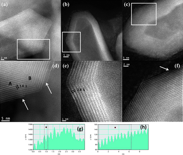 | ||
| Fig. 4 (a)–(c) Aberration-corrected STEM-HAADF image recorded from a MoS2 nanotube with various caps, (d)–(f) The close-up view of the images of the nanotubes shown in (a), (b) and (c) is revealed in (d), (e) and (f), (marked by the box), (g) line profile of the nanotube shown in (e) revealing the Mo–Mo atmoic distances to be close to 2.8 Å, (h) the line profile of the layers of the nanotube is shown in (f), The white arrows shown in (d) and (f) reveal the corners of the nanotubes, where the last atomic MoS2 layer appears to be discontinuous. | ||
In order to reproduce the main features of the structure shown in the aberration-corrected STEM micrograph, Fig. 5(c), we built a theoretical structure shown in Fig. 5(a), consisting a multiwall MoS2 nanotube of inner diameter 9.2 nm approx., and outer diameter of 13.2 nm, aproximately. For sake of simplicity, we restrict our model to just 4 concentric tubes, even if the real structures consist in at least 12 concentric tubes (as in Fig. 5(c)). All the four walls were rolled up as zigzag tubes. The innermost tube in the model structure is a zigzag (90,0) tube. The successive layers were also zigzag tubes [roll-up vectors (103,0), (116,0), (129,0)]. Fig. 5(b) corresponds to the simulated STEM micrograph image of the theoretical structure, calculated with the axis of the tube perpendicular to the electron beam. We can note that there is a fair qualitative correspondence with the real STEM image. The identification of the zigzag tubes, instead of the possible alternatives (armchair or helical tubes) is based on the comparison of the characteristic distances in the model against those measured in the real micrographs. This comparison is exemplified in Fig. 6, where a segment of the modeled nanotube has been used to calculate the STEM micrograph shown in Fig. 6(a) with a resolution similar to the one reached in the real micrograph Fig. 6(b); in this figure, the atomic rows correspond to segments of the lines that can be seen in Fig. 5(a) as being part of the walls of the tubes. Both in the real and the simulated STEM micrographs, it is possible to locate the sites of S and Mo with a resolution high enough to measure apparent interatomic distances. The distances between the Mo–Mo atoms is 2.8 Å and the distance between the layers correspond to 6.6 Å (based on the comparison of both the simulated and the experimental images). We see here that the zigzag model describes appropriately the relative positions of the S and Mo atoms. We can also note that in both images the Mo atoms – the more intense spots—vary in intensity depending on the row where they are located; this variation is atleast partially due to the differences in curvature of the tubes forming the multiwall structure: the most external tubes have less curvature, and their walls are more similar to ideal planar walls with their atomic columns perpendicular to the electron beam. In the situations where the ends of the tubes are closed, the closing of the structure is accomplished by the bending of the walls by acute angles that may be as small as 14 degrees or at large as 70 degrees (Fig. 7a,b,d,e). These bends allow changing the direction of the walls without producing faults in the structure, to the cost of generating local stresses at the vicinity of the vertex of the angle. Some of the stress may be released by small rotations of the MoS2 layers around the axis of the tube, making the tube to change from a zigzag to a helical type. Fig. 7 shows some examples of these bending, along with two models of the bending of the MoS2 layers. In the model shown in Fig. 7(c) of a bending of 27 degrees, the stress at the vertex is higher than that of the vertex in the model of Fig. 7(f), where the bending is accompanied by a twist in the MoS2 layers. Close inspection of the aberration-corrected STEM micrographs shows evidence of this kind of twists, although not as pronounced as in the model in Fig. 7(f). We attempted to construct several designs in order to close completely the multiwall tube proposed in Fig. 5(a) (trying to follow the main features of real tubes) by using just bends and twists, but our efforts were unsuccessful, because at some stage in the construction, the S–Mo–S sequence invariably got broken. It is likely that, in order to close the end of the tubes, there will be needed the inclusion of topological defects on the lattice, as suggested by Seifert et al.29 The formation of the nanotube tips was explained by the introduction of defects which inturn produce the positive and negative curvature responsible for the closure of the nanotube tips. Taking as example the case of the zigzag nanotubes, in order to induce closure the introduction of three square-like defects (SQDs) can facilitate the process, whereas in the case of armchair nanotubes, the closure can be obtained by using four SQDs and one octagonal-like defect (OLD). The OLD introduces negative curvature into the system which is balanced by the addition of one SQD (positive curvature), satisfying Euler's law analogously as in graphite. It must be noted that the closure of an armchair nanotube based on a binary hexagonal compound (like MX2 or BN) is also possible without octagonal-like defect by means of only three SQDs (ex: ZrS2 nanotubes).29
![(a) Ball-and-stick model of a multiwall MoS2 nanotube. Mo atoms appear as pink spheres, and pale yellow spheres represent S atoms. All the four walls were rolled up as zigzag tubes. The inner wall is a (90,0) tube of 9.2 nm of diameter. The successive layers were also zigzag tubes [roll-up vectors (103,0), (116,0), (129,0)], (b) STEM simulation of the tube shown in (a), with the axis of the tube perpendicular to the electron beam. (c) Real aberration-corrected STEM micrograph of a 12-walled nanotube. A partial reproduction of (b) was scaled and superposed into the micrograph in (c).](/image/article/2010/NR/c0nr00484g/c0nr00484g-f5.gif) | ||
| Fig. 5 (a) Ball-and-stick model of a multiwall MoS2 nanotube. Mo atoms appear as pink spheres, and pale yellow spheres represent S atoms. All the four walls were rolled up as zigzag tubes. The inner wall is a (90,0) tube of 9.2 nm of diameter. The successive layers were also zigzag tubes [roll-up vectors (103,0), (116,0), (129,0)], (b) STEM simulation of the tube shown in (a), with the axis of the tube perpendicular to the electron beam. (c) Real aberration-corrected STEM micrograph of a 12-walled nanotube. A partial reproduction of (b) was scaled and superposed into the micrograph in (c). | ||
![(a) STEM simulated image of a segment of the multiwall tube model presented in Fig. 6. The resolution and contrast are high enough to identify the S columns, as can be noted by the superposition of the ball and stick model (pink balls: Mo atoms; yellow balls: S atoms). Measurements were made directly on the STEM simulated image. (b) Segment of an aberration-corrected STEM micrograph, where the S columns are also identifiable. [Note that the distances between the Mo–Mo atoms is 2.8 Å and the distance between the layers correspond to 6.6 Å].](/image/article/2010/NR/c0nr00484g/c0nr00484g-f6.gif) | ||
| Fig. 6 (a) STEM simulated image of a segment of the multiwall tube model presented in Fig. 6. The resolution and contrast are high enough to identify the S columns, as can be noted by the superposition of the ball and stick model (pink balls: Mo atoms; yellow balls: S atoms). Measurements were made directly on the STEM simulated image. (b) Segment of an aberration-corrected STEM micrograph, where the S columns are also identifiable. [Note that the distances between the Mo–Mo atoms is 2.8 Å and the distance between the layers correspond to 6.6 Å]. | ||
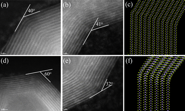 | ||
| Fig. 7 (a), (b), (d), and (e): Several bends on the walls on the walls of the MoS2 nanotubes. We found angles as small as 14 degrees and as large as 70 degrees, where the angles of 40 and 60 degrees are relatively common. (c) and (f): Two kinds of bending of a model structure; in the latter, the bending is accompanied by a twist in the MoS2 layers, which lowers the stresses on the vicinity of the vertices of the bends (pink balls: Mo atoms; yellow balls: S atoms). | ||
We have used GPA to map the rotation of the lattice fringes with respect to a region where the layers are fairly straight. We applied GPA to two different structures, and the results are shown in Fig. 8. Here, the false colors represent amount of rotation of the lattice formed by the layers forming the multiwalled tubes, with respect to some particular orientation. The scale goes from a 10 degrees clockwise rotation (deep blue color), to a 10 degrees counter-clockwise rotation (yellow). Since the rotations are defined with respect to an undistorted area, the analysis was made dividing each image into segments where the lattice fringes change in a continuous way. In the three regions, the change in the orientation of the walls was found to reach values almost as large as the maximum in the scale (10 degrees), without changing the inner structure of the lattice. Above this point, the stress generated by the distortions appear to be too large to be supported by the walls without affecting the periodicity on the MoS2 arrangement, and thus larger changes in the orientation occur by abrupt modifications in the lattice.
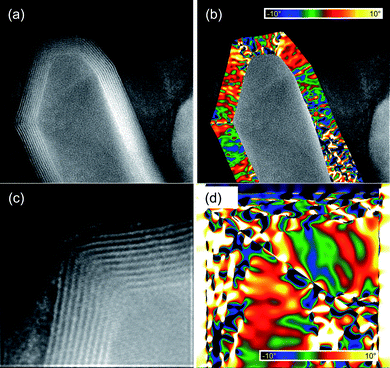 | ||
| Fig. 8 GPA of capped MoS2 nanotubes—rotation of the lattice fringes defined by the MoS2 layers forming the walls of the tubes. | ||
Shown in Fig. 9 is the aberration-corrected STEM image of the MoS2 nanotube. The arrays of Mo atoms is clearly seen from the image (bright atom contrast). A close-up view of the area marked in Fig. 9a is revealed in Fig. 9b. An overlay of Mo and S atom projection is presented on top of the image for a better understanding of the stacking of the individual atoms in the structure (Fig. 9b and c). From the images it is possible to identify not only the Mo atoms of each layer, but also the two S atoms linked to each Mo. Furthermore, it is also possible to elucidate the orientation of the S atoms which are linked to the Mo atoms wherein the linking is in a parallel manner in every layer. From this we can conclude unambiguously that the MoS2 nanotubes have the presence of the rhombohedral polytype R3m in this stacking of layers, which is unusual for MoS2 nanotubes wherein the 2H modification is commonly encountered.23 The interatomic distances between S atoms is also slightly shorter than the theoretical predicted values, being for the case of the atoms marked by arrows 3.23 ± 0.1 Å, in comparison with 3.608 Å, values which can be also understood as a consequence of the contraction between layers in that face. In the case of single-walled MoS2 nanotube bundles it was shown that the closest sulfur atoms on adjacent nanotubes are separated by 0.35(1) nm corresponding approximately to their Van der Waals diameters.30
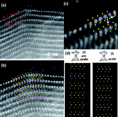 | ||
| Fig. 9 (a) Aberration-corrected STEM-HAADF images of a MoS2 nanotube. The atomic resolution image of the area marked by a dash square in (a) is shown in (c), (b) and (c) Detailed atomic distribution of the Mo and S atoms forming the layers with a projected model on top, (d) Structural models of MoS2 showing the 2H and the 3R modifications. | ||
In order to understand the atomic configuration in the layers and between the layers at these regions, the bulk crystal structures are presented in Fig. 9d: 2H, and 3R. The 2H layer stacking shows an antiparallel alignment of S–Mo–S chevrons that does not seem to fit the kind of stacking observed in the present case. However the parallel alignment of S–Mo–S chevrons produced by the projection of the 3R layer stacking provides a much better fit (compare Fig. 9b,c and d). The conclusion is that the nanotube layers are constructed from the trigonal prismatic configuration with a parallel alignment of the S–Mo–S chevrons. It is worth noting that this kind of parallel MoS2 layer stacking is not thermodynamically stable and is rarely encountered in the bulk as in the 3R-MoS2 phase.27,28,31 The images presented here provide the first direct evidence for the stacking of the Mo and S in the MoS2 nanotubes with the 3R-modification. Although the signature of this polytype was identified by carrying out X-ray diffraction and resonance Raman spectroscopy, direct imaging techniques as shown in the present case was not possible till now.21 In the present study using aberration-corrected STEM imaging we have been able to clearly identify this local stacking sequence.
4. Conclusions
A study of the MoS2 nanotubes using aberration-corrected electron microscopy along with simulated HREM images reveals various features of the capping, structure and bonding in the case of these nanotubes. The MoS2 nanotubes with various faceted caps could find important applications as field-emission sources. Previously reproducibly stable FE currents in excess of 10 mA were measured from single NT tips in vacuum. However these currents have been measured in the case of open ended nanotubes and have not yet been reported in the case of the closed nanotubes as those obtained in the present study.32 Another possibility is to use them as catalysts since these properties have not been investigated for capped nanotubes as those obtained in the present study. We are currently carrying out investigations on the catalytic properties of such capped nanotubes. The MoS2 nanotubes obtained in the present case are zigzag in nature and this opens up the possibility of the use of these nanotubes in optoelectronic devices since these structures have been shown to possess a small direct band gap.29 Finally it is worthy to remark that the elucidation of the local structural bonding revealing the 3R stacking in the nanotubes studied in this work has been observed by direct aberration-corrected electron microscopy for the first time. It is hoped that the present study will promote the use of these advanced electron microscopic techniques to improve the understanding of the structure and properties of various other nanotubes.Acknowledgements
Dr Isabel Diaz and Dr Laura Pascual (ICP-CSIC, Spain) for permitting the usage of JEOL 2100 F (FEG-TEM) microscope.References
- M. S. Wang, Q. Chen and L. M. Peng, Small, 2008, 4, 1907–1912 CrossRef CAS.
- M. S. Wang, J. Y. Wang and L. M. Peng, Appl. Phys. Lett., 2006, 88, 243108-1–243108-3.
- A. R. Ashrafi, M. Hamadanian, Z. Tavangara and H. Sabzyan, Digest Journal of Nanomaterials and Biostructures, 2009, 4, 319–322 Search PubMed.
- (a) S. lijima, T. Ichihashi and Y. Ando, Nature, 1992, 356, 776–778 CrossRef CAS; (b) S. Iijima, P. M. Ajayan and T. Ichihashi, Phys. Rev. Lett., 1992, 69, 3100–3103 CrossRef CAS.
- H. Dai, J. H. Hafner, A. G. Rinzler, D. T. Colbert and R. E. Smalley, Nature, 1996, 384, 147–150 CrossRef CAS.
- J. A. Harrison, S. J. Stuart, D. H. Robertson and C. T. White, J. Phys. Chem. B, 1997, 101, 9682–9685 CrossRef CAS.
- (a) R. Tenne and G. Seifert, Annu. Rev. Mater. Res., 2009, 39, 387–413 CrossRef CAS; (b) R. Tenne, M. Remškar, A. Enyashin and G. Seifert, Topics in Applied Physics, ed. C. Ascheron, 2008, Springer-Verlag, Berlin, vol. 111, pp. 631–671 Search PubMed.
- (a) C. N. R. Rao and A. Govindaraj, Adv. Mater., 2009, 21, 4208–4233 CrossRef CAS; (b) C. N. R. Rao and M. Nath, Dalton Trans., 2003, 1–24 RSC; (c) M. Remškar, Adv. Mater., 2004, 16, 1497–1504 CrossRef CAS.
- R. Tenne and C. N. R. Rao, Nanotechnology of Carbon and Related Materials, Philos. Trans. R. Soc. London, Ser. A, 2004, 362, 2099–2125 CrossRef CAS.
- Y. Saito and M. Maida, J. Phys. Chem. A, 1999, 103, 1291–1293 CrossRef CAS.
- R. Ma, Y. Bando, T. Sato and K. Kurashima, Chem. Mater., 2001, 13, 2965–2971 CrossRef CAS.
- O. R. Lourie, C. R. Jones, B. M. Bartlett, P. C. Gibbons, R. S. Ruoff and W. E. Buhro, Chem. Mater., 2000, 12, 1808–1810 CrossRef CAS.
- M. Terrones, W. K. Hsu, H. Terrones, J. P. Zhang, S. Ramos, J. P. Hare, R. Castillo, K. Prassides, A. K. Cheetham, H. W. Kroto and D. R. M. Walton, Chem. Phys. Lett., 1996, 259, 568–573 CrossRef CAS.
- (a) Y. Q. Zhu, W. K. Hsu, H. Terrones, N. Grobert, B. H. Chang, M. Terrones, B. Q. Wei, H. Kroto, D. R. M. Walton, C. B. Boothroyd, I. Kinloch, G. Z. Chen, A. H. Windled and D. J. Fray, J. Mater. Chem., 2000, 10, 2570–2577 RSC; (b) Y. Q. Zhu, W. K. Hsu, M. Terrones, S. Firth, N. Grobert, R. J. H. Clark, H. W. Kroto and D. R. M. Walton, Chem. Commun., 2001, 121–122 RSC; (c) Y. Q. Zhu, W. K. Hsu, M. Terrones, S. Firth, N. Grobert, R. J. H. Clark, H. W. Kroto and D. R. M. Walton, Chem. Phys. Lett., 2001, 342, 15–21 CrossRef CAS.
- M. Bar Sadan, L. Houben, A. N. Enyashin, G. Seifert and R. Tenne, Proc. Natl. Acad. Sci. U. S. A., 2008, 105, 15643–15648 CrossRef CAS.
- M. Bar- Sadan, M. Heidelmann, L. Houben and R. Tenne, Appl. Phys. A: Mater. Sci. Process., 2009, 96, 343–348 CrossRef CAS.
- (a) HREM Research Inc., http://www.hremresearch.com; (b) K. Ishizuka, Ultramicroscopy, 2002, 90, 71–83 CrossRef CAS.
- M. J. Hÿtch, E. Snoeck and R. Kilaas, Ultramicroscopy, 1998, 74, 131–146 CrossRef CAS.
- N. Grobert, M. Terrones, A. J. Osborne, H. Terrones, W. K. Hsu, S. Trasobares, Y. Q. Zhu, J. P. Hare, H. W. Kroto and D. R. M. Walton, Appl. Phys. A: Mater. Sci. Process., 1998, 67, 595–598 CrossRef.
- J. Sloan, J. L. Hutchison, R. Tenne, Y. Feldman, T. Srilina and M. Homyonfer, J. Solid State Chem., 1999, 144, 100–117 CrossRef CAS.
- (a) M. Remškar, Z. Škraba, C. Ballif, R. Sanjinés and F. Lévy, Surf. Sci., 1999, 433–435, 637–641 CrossRef CAS; (b) M. Viršek, A. Jesih, I. Miloševic, M. Damnjanovic and M. Remškar, Surf. Sci., 2007, 601, 2868–2872 CrossRef CAS.
- Y. Mastai, M. Homyonfer, A. Gedanken and G. Hodes, Adv. Mater., 1999, 11, 1010–1013 CrossRef CAS.
- H. A. Therese, N. Zink, U. Kolb and W. Tremel, Solid State Sci., 2006, 8, 1133–1137 CrossRef CAS.
- J. Chen, S. L. Li, Q. Xu and K. Tanaka, Chem. Commun., 2002, 1722–1723 RSC.
- W. K. Hsu, B. H. Chang, Y. Q. Zhu, W. Q. Han, H. Terrones, M. Terrones, N. Grobert, A. K. Cheetham, H. W. Kroto and D. R. M. Walton, J. Am. Chem. Soc., 2000, 122, 10155–10158 CrossRef CAS.
- (a) F. L. Deepak, A. Mayoral and M. Jose Yacaman, Mater. Chem. Phys., 2009, 118, 392–397 CrossRef CAS; (b) F. L. Deepak, A. Mayoral and M. J. Yacáman, Appl. Phys. A: Mater. Sci. Process., 2009, 96, 861–867 CrossRef CAS.
- M. Bar Sadan, L. Houben, S. G. Wolf, A. Enyashin, G. Seifert, R. Tenne and K. Urban, Nano Lett., 2008, 8, 891–896 CrossRef.
- A. N. Enyashin, M. Bar-Sadan, J. Sloan, L. Houben and G. Seifert, Chem. Mater., 2009, 21, 5627–5636 CrossRef CAS.
- (a) G. Seifert, H. Terrones, M. Terrones, G. Jungnickel and T. Frauenheim, Phys. Rev. Lett., 2000, 85, 146–149 CrossRef CAS; (b) V. V. Ivanovskaya, A. N. Enyashin, N. I. Medvedeva, Y. N. Makurin and A. L. Ivanovskii, Internet Electronic Journal of Molecular Design, 2003, 2, 499–510 Search PubMed.
- M. Remškar, A. Mrzel, Z. Skraba, A. Jesih, M. Ceh, J. Demsÿar, P. Stadelmann, F. Levy and D. Mihailovic, Science, 2001, 292, 479–481 CrossRef CAS.
- (a) M. Remškar, A. Mrzel, M. Viršek and A. Jesih, Adv. Mater., 2007, 19, 4276 CrossRef CAS; (b) M. Remškar, M. Viršek and A. Mrzel, Appl. Phys. Lett., 2009, 95, 133122–133122-3 CrossRef.
- V. Nemanič, M. Žumer, B. Zajec, J. Pahor, M. Remškar, A. Mrzel, P. Panjan and D. Mihailovič, Appl. Phys. Lett., 2003, 82, 4573–4575 CrossRef CAS.
Footnote |
| † Electronic supplementary information (ESI) available: Synthesis and structure of MoO3 nanobelts and MoS2 nanotubes. See DOI: 10.1039/c0nr00484g |
| This journal is © The Royal Society of Chemistry 2010 |