
Designing barrier-free metal/MoS2 contacts through electrene insertion†
Mohammad
Rafiee Diznab
 a,
Adrian F.
Rumson
b,
Jesse
Maassen
*a and
Erin R.
Johnson
*ab
a,
Adrian F.
Rumson
b,
Jesse
Maassen
*a and
Erin R.
Johnson
*ab
aDepartment of Physics and Atmospheric Science, Dalhousie University, 6310 Coburg Road, Halifax, Nova Scotia B3H 4R2, Canada. E-mail: jmaassen@dal.ca
bDepartment of Chemistry, Dalhousie University, 6243 Alumni Crescent, Halifax, Nova Scotia B3H 4R2, Canada. E-mail: erin.johnson@dal.ca
First published on 22nd April 2024
Abstract
Transition-metal dichalcogenides (TMDCs), including MoS2, have great potential in electronics applications. However, achieving low-resistance metal contacts is a challenge that impacts their performance in nanodevices due to strong Fermi-level pinning and the presence of a tunnelling barrier. As a solution, we explore a strategy of inserting monolayers of alkaline-earth sub-pnictide electrenes with a general formula of [M2X]+e− (M = Ca, Sr, Ba; X = N, P, As, Sb) between the TMDC and the metal. These electrenes possess two-dimensional sheets of charge on their surfaces that can be readily donated when interfaced with a TMDC semiconductor, thereby lowering its conduction band below the Fermi level and eliminating the Schottky and tunnelling barriers. In this work, density-functional theory (DFT) calculations were performed for metal/electrene/MoS2 heterojunctions for all stable M2X electrenes and both Au and Cu metals. To identify the material combinations that provide the most effective Ohmic contact, the charge transfer, band structure, and electrostatic potential were computed. Linear correlations were found between the charge donated to the MoS2 and both the electrene surface charge and work function. Overall, Ca2N appears to be the most promising electrene for achieving an Ohmic metal/MoS2 contact due to its high surface charge density.
1 Introduction
The field of nanoelectronics is poised to undergo a major revolution with the introduction of novel two-dimensional (2D) semiconductor materials. Monolayer transition-metal dichalcogenides (TMDCs) represent a pioneering family of materials in this regard, with MoS2 serving as their leading member. The stunning features of TMDC-based transistors, such as high mobility,1 extremely short channel lengths,2 high on/off ratio,3 and low sub-threshold swing,4 make this class of materials well suited for electronic device applications. However, high metal/semiconductor contact resistance has inhibited the efficacy of TMDC-based transistors.1,5–7 The high contact resistance is primarily caused by (i) the Schottky barrier and Fermi-level pinning, despite the lack of dangling or incomplete bonds on the surface of the TMDC,8–11 and (ii) the tunnelling barrier caused by the van der Waals (vdW) gap at the metal/TMDC interface.5,12–14The choice of metal plays an important role in the performance of 2D contacts. For some metal/TMDC interfaces, such as Pd/MoS2, overlap of metal and semiconductor states contributes to electron or hole injection, so that negligible tunnelling barriers are feasible.6,13 One way to fully overcome the tunnelling barrier is to choose specific metals that can form covalent bonds with the TMDC layer, e.g., Ti when interfaced with MoS2.12,15–17 However, such bonding results from strong hybridization of the metal and semiconductor orbitals, which can potentially disrupt the original MoS2 states and deteriorate the sheet resistivity of the semiconductor.5,13 That being said, hybridization of the MoS2 energy bands with the semimetallic materials bismuth and antimony has been demonstrated as one of the best strategies to push the contact resistance towards the quantum limit.18,19
Another current strategy to develop practical TMDC-based devices involves introducing an intermediate layer between the metal and 2D semiconductor to address both Fermi-level pinning and tunnelling barrier issues.9,20–25 One major cause of Fermi-level pinning in 2D metal contacts involving MoS2 is the production of gap states, mainly of Mo d-orbital character.11 Based on density-functional theory (DFT) calculations, we previously proposed that the insertion of a Ca2N monolayer not only removes the Fermi-level pinning, but also eliminates both Schottky and tunnelling barriers, for a model Au/Ca2N/MoS2 heterostructure.20Fig. 1 (top) shows the atomic configuration and a schematic illustration of the electronic band diagram of a proposed Au/Ca2N/MoS2 interface. Here, ΦAu and ΦCa2N are the work functions of the metal and the electrene, XMoS2 is the electron affinity of the semiconductor, and Evac and EF are the vacuum and Fermi levels, respectively. The conduction and valence bands of MoS2 are also shown as Ec and Ev. Due to charge transfer from the Ca2N monolayer, the MoS2 is negatively doped so that its conduction band edge falls below the Fermi level (Ec < EF), removing the Schottky barrier for electron transport.
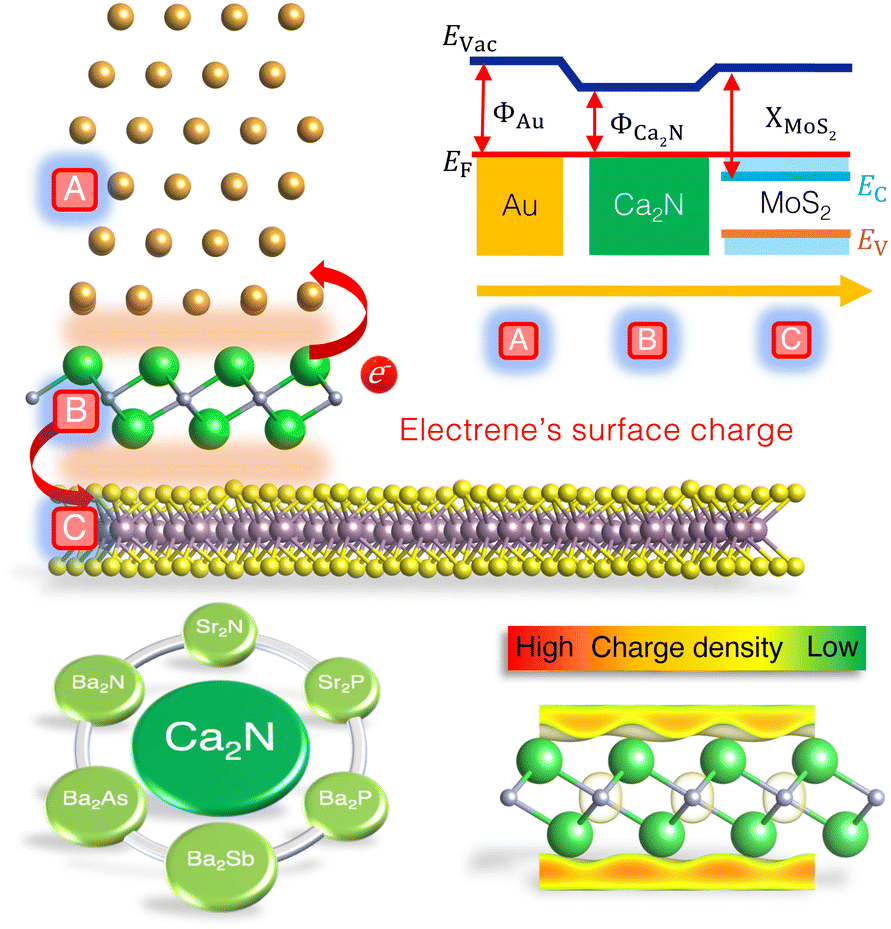 | ||
| Fig. 1 Top: Schematic design of the Au/MoS2 interface with monolayer Ca2N as an intermediate layer. The associated band diagram indicates the removal of the Schottky barrier upon metallization of the MoS2 bands. Bottom: List of all stable M2X electrides, along with a 3D representation of the electrene's surface charge. | ||
Ca2N is a 2D electride;26,27 this is an ionic material in which the anion is an excess electron that is localized to the interstitial regions between the atomically thin, positively charged, layers of the material. Upon exfoliation, the anionic electrons form delocalized 2D sheets of charge surrounding the surface of the monolayer, now termed an electrene.28,29 The bottom-right panel of Fig. 1 illustrates the surface charge density of an electrene. These surface states could potentially lead to high charge transport, allowing electrenes to find utility in device applications. Ca2N is only one member of the family of 2D electrides with a general chemical formula of M2X (M = Ca, Sr, Ba; X = N, P, As, Sb). The crystal structures of bulk Ca2N, Sr2N, and Ba2N,27,30 as well as few-layer Ca2N,28 have been experimentally characterized, while the others are proposed to be layered electrides on the basis of DFT studies.28–41 We have previously investigated periodic trends in the electronic, structural, and transport properties of the corresponding monolayer and bilayer electrenes.42
In this work, we employ DFT to investigate various electrenes in contact with both Au and Cu metals and MoS2 to determine which material is the most promising for eliminating the Schottky and tunnelling barriers in metal/MoS2 contacts. In particular, we determine the extent to which MoS2 conduction bands become metallized following electrene insertion and analyze the electrostatic potential at the interfaces, which should shed light on electron transport across these contacts. We also identify various correlations between monolayer electride characteristics, such as surface charge densities, and the improved charge transfer and barrier lowering that occurs at the metal/electrene/MoS2 interfaces.
2 Computational methods
2.1 DFT calculations
All DFT calculations were performed with the Quantum ESPRESSO program,43,44 using the Perdew–Burke–Ernzerhof (PBE) exchange–correlation functional,45 the projector augmented-wave (PAW) method,46,47 and periodic boundary conditions. Dispersion interactions were treated with Grimme's D3BJ pairwise dispersion scheme48 with Becke–Johnson damping.49,50 Calculations for all metal/electrene/MoS2 structures used plane-wave cutoff energies of 80 Ry and 1200 Ry for the wave function and electron density, respectively, and a k-point grid density of 0.03 × 2π Å−1. In order to avoid interactions between layers, we adopt a 20 Å vacuum region. The Methfessel–Paxton (MP) smearing method51 was used to integrate the Brillouin zone with a smearing width of 0.1 eV. Bader charge analysis was performed using the Bader52–54 code via post-processing of the DFT electron density.2.2 Heterostructure design
After fully relaxing the atomic positions and lattice constants of the isolated MoS2 monolayer, electrene monolayers, and metal slabs, we employed VASPKIT55 to build all the metal/MoS2 and metal/electrene/MoS2 heterostructures. Two criteria were considered: (i) the MoS2 layer in all heterostructures is not strained to allow direct comparison between all the interfaces and (ii) the strain on both the electrene layer and the metal slab is under 3.5% for all cases, except for Au/Ba2Sb/MoS2, for which there is 4.3% strain for the electrene. Tables S1 and S2 (ESI†) summarize the number of atoms and the in-plane lattice constants for each heterojunction, as well as the percent strains on the electrene and metal slabs. The heterostructure geometries were relaxed with respect to the atomic positions, subject to fixed lattice constants, until the force on each atom was less than 0.1 meV Å−1. Additional geometry relaxations were also performed for the free metal slabs and electrene monolayers using the same lattice constants as the corresponding heterojunctions.3 Results and discussion
3.1 Exfoliation energies
The structural properties of the studied metal/electrene/MoS2 heterostructures, including the average interlayer distances, are summarized in Table S2 (ESI†). Overall, the electrene/MoS2 interlayer distances are found to be smaller than the sum of the van der Waals radii of the sulfur and alkaline earth metal atoms, taking values of 1.73, 2.41, 2.63, and 2.71 Å, for S, Ca, Sr, and Ba respectively.56 This reflects the ionic (rather than vdW) nature of these contacts.To assess the stabilities of the various heterostructures, as well as to quantify the relative importance of strain, ionic binding (from the base density functional), and dispersion interactions, their exfoliation energies were computed. Here, the unstrained exfoliation energy is defined as the energy required to infinitely separate the three materials in the heterojunction:
| Eunstrexfo = Eunstrmetal + Eunstrelectrene + EMoS2 − Emetal/electrene/MoS2. | (1) |
| Estrexfo = Estrmetal + Estrelectrene + EMoS2 − Emetal/electrene/MoS2. | (2) |
| Estrain = Estrmetal + Estrelectrene − Eunstrmetal − Eunstrelectrene. | (3) |
The exfoliation energies in Table 1 show that formation of the metal/electrene/MoS2 interfaces is energetically favourable, and the exfoliation energies are much higher than for the Au/MoS2 and Cu/MoS2 interfaces. This is expected due to the high charge transfer from the electrene to the MoS2 and the metal slab (vide infra) resulting in strong ionic bonding, as is evident from the large base-functional contributions to the exfoliation energies (ranging from 49–77% for the strained exfoliation energies). The relative importance of the ionic interactions is largest for the light electrenes (Ca2N, Sr2N, and Sr2P), with the dispersion contributions being more significant for the heavier electrenes containing barium, particularly for Ba2Sb. From the results in Table 1, we also note that there is generally reduced dispersion binding for Cu as opposed to Au, as expected from the greater atomic size and polarizability of Au. Finally, the strain energies are typically smaller for the Cu interfaces, due to reduced strain on the metal.
| Electrene | None | Ca2N | Sr2N | Sr2P | Ba2N | Ba2P | Ba2As | Ba2Sb |
|---|---|---|---|---|---|---|---|---|
| Au/electrene/MoS2 | ||||||||
| E exfo,unstr | 3.5 | 196.6 | 181.9 | 147.0 | 237.1 | 169.0 | 172.0 | 208.8 |
| E strain | 48.2 | 49.7 | 47.7 | 46.6 | 3.0 | 46.7 | 49.5 | 52.5 |
| E exfo,str | 51.7 | 245.7 | 229.6 | 193.6 | 240.1 | 215.7 | 221.5 | 261.3 |
| E base,str | −7.8 | 179.5 | 162.6 | 144.7 | 142.2 | 135.8 | 132.1 | 128.5 |
| E disp,str | 59.5 | 66.2 | 67.0 | 48.9 | 97.9 | 79.9 | 89.5 | 132.8 |
| Cu/electrene/MoS2 | ||||||||
| E exfo,unstr | 59.8 | 178.1 | 198.2 | 155.5 | 192.2 | 151.1 | 162.8 | 240.2 |
| E strain | 36.7 | 17.0 | 8.8 | 16.3 | 23.5 | 35.8 | 33.9 | 7.5 |
| E exfo,str | 96.5 | 195.2 | 207.0 | 171.8 | 215.7 | 187.0 | 196.8 | 247.6 |
| E base,str | 21.9 | 145.1 | 139.3 | 133.9 | 127.9 | 108.5 | 113.2 | 122.9 |
| E disp,str | 74.6 | 50.0 | 83.3 | 37.9 | 87.9 | 78.5 | 83.6 | 124.8 |
As shown in Table 1, all metal/electrene/MoS2 contacts have much higher binding energies than other high-efficiency 2D TMDC contacts. For example, PtTe2/MoS2 and graphene/MoS2 have binding energies of 12.6 meV Å−2 and 0.7 meV Å−2,57 respectively. This indicates that the metal/electrene/MoS2 contact should have higher thermal stability, and the stronger interlayer interactions should promote better charge-carrier injection.
3.2 Bands, densities of states, and charge transfer
Images of the interfaces with inserted electrenes, as well as plots of their electronic band structures, densities of MoS2 states, and electrostatic potentials, are collected in Fig. S4–S17 (ESI†). We take the two metal/Ca2N/MoS2 heterostructures as illustrative examples, with the results shown in Fig. 2. The interface structures are shown in Fig. 2(a) and (e), for Au and Cu, respectively. Panels (b) and (f) show the computed band structures, decomposed according to contributions from each component material. The densities of MoS2 states are shown in Fig. 2(c) and (g). Integrating the density of MoS2 states from a particular minimum energy (Emin, below which DMoS2 is nearly zero, selected to be −0.5 eV in this work) up to the Fermi energy can reveal the extent of charge doping of the MoS2 layer (QMoS2): | (4) |
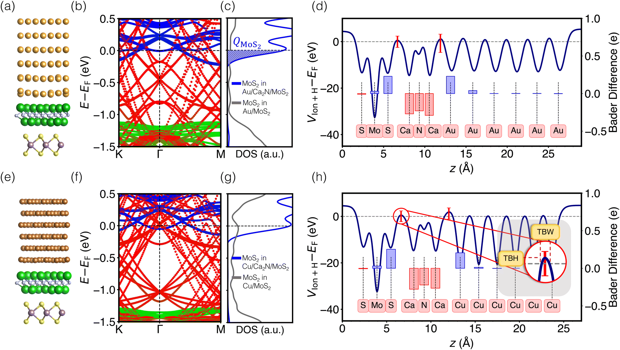 | ||
| Fig. 2 (a) Optimized structure, (b) material-projected band structure, (c) densities of MoS2 states per MoS2 formula unit, and (d) electrostatic potential for the Au/Ca2N/MoS2 interface. Panels (e)–(h) present the same quantities for the Cu/Ca2N/MoS2 interface. Metal bands are coloured red, Ca2N bands are coloured green, and MoS2 bands are coloured blue. The shaded region of the DOS plot corresponds to QMoS2. In the potential plots, the red bars indicate the range of values at the maximum point within the interface regions. The results are overlaid with the differences in Bader atomic charges for the heterostructures, relative to the separated materials. Positive (negative) values indicate accumulation (depletion) of electron density. | ||
To understand the changes in electronic structure upon electrene insertion, comparison must be made with data for the the Au/MoS2 and Cu/MoS2 interfaces, shown in Fig. S1 (ESI†). These contacts have already been extensively studied using density-functional calculations,9,11,58,59 so we only briefly discuss some of their most important features. Consistent with previous findings, our results indicate that MoS2 physisorbs on Au, but chemisorbs on Cu. Carriers at the Au/MoS2 interface experience a 0.5 eV Schottky barrier and a 3.0 eV tunnelling barrier. For the Cu/MoS2 interface, electrons that overcome a 0.4 eV Schottky barrier face only a 0.7 eV tunnelling barrier and can travel through some fraction of the interface without tunnelling.
As shown in Fig. 2(b) and (f), Ca2N insertion shifts the MoS2 conduction band minimum to −0.2 eV below the Fermi level, meaning that the Schottky barrier is eliminated. This occurs due to electron transfer from the Ca2N to the MoS2, which is apparent from comparison with the isolated Ca2N band structure (Fig. S18–S21, ESI†), as the heterojunction band structures no longer include any Ca2N surface states near the Fermi level. For both Au- and Cu-based heterojunctions, evaluation of the Bader charges (Table S4, ESI†) shows that ca. 0.8 e− per Ca2N formula unit is transferred, partially to the metal and partially to the MoS2. The observation of fractional charge transfer is potentially a consequence of delocalization error,60,61 which stems from using a generalized gradient approximation (PBE) in this work. Based on a comparison of PBE and HSE0662 band structures for the bare Ca2N/MoS2 interface without any metal (see Fig. S3, ESI†), it is expected that the charge transfer would increase to nearly a full electron per Ca2N formula unit if hybrid functionals were to be employed. However, this increase in charge transfer is not expected to qualitatively impact our results and, beyond being far too computationally expensive with planewave basis sets to apply to the full metal/electrene/MoS2 interfaces, hybrid functionals are not recommended for metals.
Overall, the findings discussed for Ca2N above are general based on our analysis of band structures and Bader charges. For all interfaces considered, electrene insertion at the metal/MoS2 interfaces results in electron transfer from the electrene to the MoS2 (see Table S4, ESI†), and a concomitant energy lowering of the MoS2 conduction band edge (see Table S5, ESI†) to below the Fermi level. Thus, for all metal/electrene/MoS2 heterostructures, electrene insertion negatively dopes the MoS2, resulting in the removal of the Schottky barrier and unpinning of the Fermi level with no mid-gap states introduced, as shown in Fig. S4–S17 (ESI†).
In addition to providing a nearly barrierless interface to charge carriers, a good metal contact should also result in minimal distortion of the TMDC states, so as to not deteriorate the semiconductor sheet resistivity. Upon contact formation, the MoS2 band gap is found to change by up to only ±0.15 eV relative to that of the pristine MoS2 monolayer (calculated to be 1.72 eV), depending on the choice of the electrene and metal (see Table S5, ESI†). This relatively small modification of the band gap should preserve the resistivity of contacted MoS2.
3.3 Electrostatic potential profiles and tunneling
While the band structure and DOS plots reveal the promise of the electrene insertion strategy to remove the Schottky barrier, analysis of the electrostatic potential profile of the interface provides information regarding the presence or absence of a tunnelling barrier. Comparison of the Au/Ca2N/MoS2 electrostatic potential profile in Fig. 2(d) with the result for the Au/MoS2 heterojunction in Fig. S1 (ESI†) illustrates how Ca2N insertion reduces the tunneling barrier at the interface to ca. 0.5 eV, compared to ca. 3.0 eV for Au/MoS2 without the electrene. Ca2N insertion at Cu/MoS2 leads to a similarly small tunneling barrier of ca. 0.5 eV.In the electrostatic potential plots in Fig. 2(d) and (h), the red bars indicate the range of values (in the x, y plane) that occur at the z position having the highest average potential within the interface regions. The minima of the red bars extend below the Fermi level, indicating Ohmic contact behaviour for some regions of the interface. By projecting the potential profile at the interface into the real-space 2D plane, it is revealed that there is a correlation between the location of the alkaline-earth metal atoms and the Ohmic areas of the interface. For example, for the Au/Ca2N/MoS2 heterostructure, the minima of the electrostatic potential occur at the same x, y positions as the calcium sites, while the secondary minima correspond to sulfur locations (see Fig. S4(f), ESI†). This is the case for all metal/electrene/MoS2 heterostructures considered, as shown in Fig. S4–S17 (ESI†), which allows electrons injected from the metal contact to more easily make their way through to the TMDC.
To ensure that our predictions of high charge transfer and low tunneling barriers are not artifacts of a particular interface geometry, we performed additional calculations for the Cu/Ca2N/MoS2 interface, in which the MoS2 layer was slid over the Ca2N. Specifically, the MoS2 layer was shifted uniformly in the a and b cell directions in increments of 0.2, 0.4, 0.6, and 0.8 times the in-plane lattice vectors and the resulting structures geometry optimized. Relative energies, Fermi energies, charge transfer, and Ohmicity fraction (vide infra), as well as tunneling barrier heights and widths, are given in Table S6 (ESI†). All show only very minor variations with the fractional sliding coordinate. These results provide confidence that our calculations have used the most stable configurations in terms of MoS2 sliding, and that our predictions of favourable interface properties are general and not just a feature of one possible geometry.
3.4 Comparison of electrenes
Next, we consider trends involving the extent of charge transfer for all seven electrenes to assess which is the most promising. Fig. 3(a) and (b) show the correlation of QMoS2 values with the surface charges and the work functions (Φm) of various monolayer electrenes computed in our previous work.42 The surface charges of the monolayer electrenes were obtained from the planar average of the integrated local density of states (ILDOS) along the z-axis, integrated over energy from the bottom of the surface bands up to the Fermi level. The averaged ILDOS was then integrated along the z-axis from the outermost metal atom to the vacuum region (where the ILDOS reaches zero) to give
  . The almost linear correlation between QMoS2 and
  indicates that electrenes with higher surface charge densities can donate more charge to the adjacent semiconductor layer.
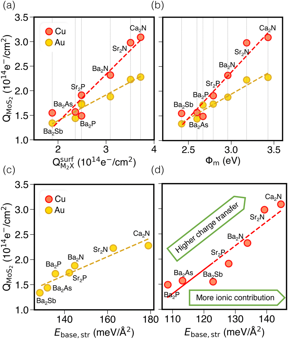 | ||
Fig. 3 (a) Correlation of QMoS2 and  in Au and Cu-based interfaces. (b) Correlation of QMoS2 and the monolayer electrene work function (Φm). Also shown are correlations between the base-functional (ionic) component of the exfoliation energy and QMoS2 for Au (c) and Cu (d) interfaces, respectively. in Au and Cu-based interfaces. (b) Correlation of QMoS2 and the monolayer electrene work function (Φm). Also shown are correlations between the base-functional (ionic) component of the exfoliation energy and QMoS2 for Au (c) and Cu (d) interfaces, respectively. | ||
Fig. 3(b) shows a positive correlation between QMoS2 and the work function, Φm, computed42 for the monolayer electrene. This result is somewhat counterintuitive, since lower work function materials may be expected to promote more electron transfer to the semiconductor. However, we previously found that electrenes with higher work functions have a greater surface charge density42 (i.e. more charge available in the surface states) that is available to donate. Overall, electrenes composed of smaller and chemically harder metal and pnictogen atoms show stronger electrostatic stabilization of the anionic surface charge by the cationic layer. This gives rise to greater surface charge density and tighter binding of the surface states, as quantified by smaller average distances of the surface charge from the alkaline earth metal cations and by larger work functions. Thus, a higher work function implies that the electrene has more charge available to donate to the MoS2, explaining the greater QMoS2 values for the corresponding metal/electrene/MoS2 interfaces.
It should be noted that separate correlations are observed for Au and Cu in Fig. 3(a) and (b) due to the differing electronegativities of these metals. Since Cu is less electronegative than Au, it will accept less charge. Indeed, the computed Bader charges in Table S4 (ESI†) illustrate that, for any specified electrene, QBaderAu > QBaderCu. As a result, more charge is available to be donated to the MoS2 layer in the case of a Cu surface, such that QMoS2 values are higher for Cu/electrene/MoS2 heterostructures compared to their Au counterparts, regardless of the choice of electrene. Hence, the MoS2 layer receives a greater fraction of the electrene's surface charge when in contact with the less electronegative metal.
By considering only the base-functional contribution, Ebase,str, we can also correlate the ionic (i.e. non-dispersion) part of the exfoliation energy and the metallization of the semiconductor (QMoS2), as shown in Fig. 3(c) and (d). Strong linear correlations are observed for both Au/electrene/MoS2 and Cu/electrene/MoS2 heterostructures. Ca2N and Sr2N, which possess the largest electrene surface charge densities, also have the highest ionic contributions to the exfoliation energies for these interfaces. The results are in line with the periodic trend in the exfoliation energies of the corresponding bulk electrides.42
Fig. 4 schematically depicts the measures used for assessing contacts in this study, which are also collected in Table S7 (ESI†). Panel (a) shows that the extent of charge transfer, QMoS2, is greatest for Ca2N, followed by Sr2N and Ba2N. This is the same trend observed for the monolayer surface charge, as noted above. Values are also shown for the two metal/MoS2 interfaces for comparison, where there is still a Schottky barrier present and the QMoS2 values quantify the charge occupying mid-gap states up to 0.5 eV below the Fermi level. This is in contrast to the metal/electrene/MoS2 interfaces, where there are no mid-gap states present and QMoS2 quantifies the metallization of the MoS2 conduction band.
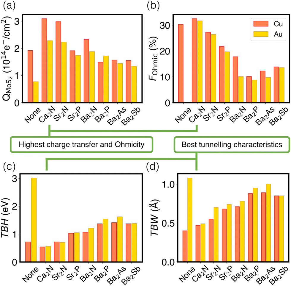 | ||
| Fig. 4 Bar graphs showing the variation of four figures of merit as a function of the electrene in the metal/electrene/MoS2 contacts. The individual plots show: (a) the charge transfer to MoS2, QMoS2; (b) the fraction of the contact area that is Ohmic, FOhmic; (c) the tunneling barrier height, TBH; and (d) tunneling barrier width, TBW. Results for the metal/MoS2 interfaces with no electrene are shown for comparison; note that the QMoS2 for these two cases results from mid-gap states rather than from the MoS2 conduction band. | ||
The Ohmicity of metal/electrene/MoS2 contacts can be quantified from analysis of the electrostatic potential at the electrene/MoS2 interface. The Ohmicity fraction is defined as
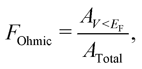 | (5) |
Tunnelling characteristics of the contacts are also compared in Fig. 4(c) and (d) for all metal/electrene/MoS2 configurations. It is imperative that the tunnelling barrier be small enough to maximize the transmission probability. Regardless of the choice of the metal, Ca2N manifests the lowest TBH and TBW, followed by Sr2N and Sr2P. Also, consistent with the FOhmic results, Cu-based heterostructures show slightly smaller TBWs compared to their Au counterparts. Using the WKB approximation63 (see Section 4 of the ESI†), the calculated tunnelling specific resistivity of Au/MoS2 is 1.2 × 10⁻⁹ Ω cm2, with a tunnelling probability of ≤1%. As such, insertion of monolayer Ca2N, which raises the tunneling probability to >20%, lowers the contact resistivity by almost two orders of magnitude. However, since the Cu/MoS2 tunnelling barrier is negligible, the electrene insertion strategy is most helpful with the elimination of the Schottky barrier in this case. Following the same trends as extracted from the electrostatic potential plots, Ca2N shows the highest tunnelling probability and lowest tunnelling specific resistivity of all the electrenes considered, followed by Sr2N.
Finally, it is insightful to compare the metal/electrene/MoS2 tunnelling characteristics with those of the elemental semimetal contacts of MoS2, which currently set the gold standard of 2D contacts. For example, Sb(01![[1 with combining macron]](https://www.rsc.org/images/entities/char_0031_0304.gif) 2)/MoS2 and Sb(0001)/MoS2 show TBWs of 1.35 Å and 1.39 Å, respectively,18 whereas the TBWs of {Au,Cu}/Ca2N/MoS2 are ∼0.5 Å. The tunnelling barrier height of {Au,Cu}/Ca2N/MoS2 is also significantly lower than that of Sb(012)/MoS2 (3.05 eV) and Sb(0001)/MoS2 (3.13 eV).18 Our metal/electrene/MoS2 interfaces also show better tunnelling characteristics than a Bi(0001)/MoS2 interface with a TBW and TBH of 1.66 Å and 3.6 eV, respectively.19
2)/MoS2 and Sb(0001)/MoS2 show TBWs of 1.35 Å and 1.39 Å, respectively,18 whereas the TBWs of {Au,Cu}/Ca2N/MoS2 are ∼0.5 Å. The tunnelling barrier height of {Au,Cu}/Ca2N/MoS2 is also significantly lower than that of Sb(012)/MoS2 (3.05 eV) and Sb(0001)/MoS2 (3.13 eV).18 Our metal/electrene/MoS2 interfaces also show better tunnelling characteristics than a Bi(0001)/MoS2 interface with a TBW and TBH of 1.66 Å and 3.6 eV, respectively.19
4 Conclusion
To summarize our results, considering all four figures of merit employed (QMoS2, FOhmic, TBW, and TBH), we find that Ca2N is consistently the most favourable electrene material to insert to eliminate Schottky and tunnelling barriers across the Au/MoS2 or Cu/MoS2 interfaces, owing to its high surface charge density. Sr2N takes second place for all figures of merit and also appears to be promising, although somewhat less so than Ca2N. Finally, since Cu is less electronegative than Au, it accepts less charge from the electrene layer, resulting in a more metallized MoS2, regardless of the choice of electrene. Insertion of electrides appears to be a highly promising strategy to generate n-type (but not p-type) Ohmic contacts since they are excellent reducing agents (but not oxidizing agents). Provided the practical experimental challenges of electrene exfoliation can be overcome,28 including addressing problems with air and water stability,64 insertion of 2D electrenes should be a promising approach to improve electron transport across metal/TMDC heterojunctions.Conflicts of interest
There are no conflicts to declare.Acknowledgements
This research was supported by the Semiconductor Research Corporation (SRC) and the Digital Research Alliance of Canada.References
- S. Das, H.-Y. Chen, A. V. Penumatcha and J. Appenzeller, Nano Lett., 2013, 13, 100–105 CrossRef CAS PubMed.
- L. Xie, M. Liao, S. Wang, H. Yu, L. Du, J. Tang, J. Zhao, J. Zhang, P. Chen and X. Lu, et al. , Adv. Mater., 2017, 29, 1702522 CrossRef PubMed.
- B. Radisavljevic, A. Radenovic, J. Brivio, V. Giacometti and A. Kis, Nat. Nanotechnol., 2011, 6, 147–150 CrossRef CAS PubMed.
- X.-F. Wang, H. Tian, Y. Liu, S. Shen, Z. Yan, N. Deng, Y. Yang and T.-L. Ren, ACS Nano, 2019, 13, 2205–2212 CAS.
- A. Allain, J. Kang, K. Banerjee and A. Kis, Nat. Mater., 2015, 14, 1195–1205 CrossRef CAS PubMed.
- W. Liu, J. Kang, W. Cao, D. Sarkar, Y. Khatami, D. Jena and K. Banerjee, 2013 IEEE Intl. Electron Device Mtg., 2013, pp. 19–4 Search PubMed.
- H. Liu, A. T. Neal and P. D. Ye, ACS Nano, 2012, 6, 8563–8569 CrossRef CAS PubMed.
- C. Kim, I. Moon, D. Lee, M. S. Choi, F. Ahmed, S. Nam, Y. Cho, H.-J. Shin, S. Park and W. J. Yoo, ACS Nano, 2017, 11, 1588–1596 CrossRef CAS PubMed.
- M. Farmanbar and G. Brocks, Phys. Rev. B: Condens. Matter Mater. Phys., 2015, 91, 161304 CrossRef.
- P. Bampoulis, R. van Bremen, Q. Yao, B. Poelsema, H. J. Zandvliet and K. Sotthewes, ACS Appl. Mater. Interfaces, 2017, 9, 19278–19286 CrossRef CAS PubMed.
- C. Gong, L. Colombo, R. M. Wallace and K. Cho, Nano Lett., 2014, 14, 1714–1720 CrossRef CAS PubMed.
- I. Popov, G. Seifert and D. Tománek, Phys. Rev. Lett., 2012, 108, 156802 CrossRef PubMed.
- J. Kang, W. Liu, D. Sarkar, D. Jena and K. Banerjee, Phys. Rev. X, 2014, 4, 031005 CAS.
- T. Shen, J.-C. Ren, X. Liu, S. Li and W. Liu, J. Am. Chem. Soc., 2019, 141, 3110–3115 CrossRef CAS PubMed.
- K. Stokbro, M. Engelund and A. Blom, Phys. Rev. B: Condens. Matter Mater. Phys., 2012, 85, 165442 CrossRef.
- J. Kang, D. Sarkar, W. Liu, D. Jena and K. Banerjee, 2013 IEEE Intl. Electron Device Mtg., 2012, pp. 17–4 Search PubMed.
- L.-Y. Gan, Y.-J. Zhao, D. Huang and U. Schwingenschlögl, Phys. Rev. B: Condens. Matter Mater. Phys., 2013, 87, 245307 CrossRef.
- W. Li, X. Gong, Z. Yu, L. Ma, W. Sun, S. Gao, Ç. Köroğlu, W. Wang, L. Liu and T. Li, et al. , Nature, 2023, 613, 274–279 CrossRef CAS PubMed.
- P.-C. Shen, C. Su, Y. Lin, A.-S. Chou, C.-C. Cheng, J.-H. Park, M.-H. Chiu, A.-Y. Lu, H.-L. Tang and M. M. Tavakoli, et al. , Nature, 2021, 593, 211–217 CrossRef CAS PubMed.
- F. Kaadou, J. Maassen and E. R. Johnson, J. Phys. Chem. C, 2021, 125, 11656–11664 CrossRef CAS.
- Y. Liu, J. Guo, Y. Wu, E. Zhu, N. O. Weiss, Q. He, H. Wu, H.-C. Cheng, Y. Xu and I. Shakir, et al. , Nano Lett., 2016, 16, 6337–6342 CrossRef CAS PubMed.
- H.-J. Chuang, B. Chamlagain, M. Koehler, M. M. Perera, J. Yan, D. Mandrus, D. Tomanek and Z. Zhou, Nano Lett., 2016, 16, 1896–1902 CrossRef CAS PubMed.
- M. Farmanbar and G. Brocks, Adv. Electron. Mater., 2016, 2, 1500405 CrossRef.
- Y. Du, L. Yang, J. Zhang, H. Liu, K. Majumdar, P. D. Kirsch and D. Y. Peide, IEEE Electron Dev. Lett., 2014, 35, 599–601 CAS.
- W. S. Leong, X. Luo, Y. Li, K. H. Khoo, S. Y. Quek and J. T. Thong, ACS Nano, 2015, 9, 869–877 CrossRef CAS PubMed.
- J. L. Dye, Acc. Chem. Res., 2009, 42, 1564–1572 CrossRef CAS PubMed.
- K. Lee, S. W. Kim, Y. Toda, S. Matsuishi and H. Hosono, Nature, 2013, 494, 336–340 CrossRef CAS PubMed.
- D. L. Druffel, K. L. Kuntz, A. H. Woomer, F. M. Alcorn, J. Hu, C. L. Donley and S. C. Warren, J. Am. Chem. Soc., 2016, 138, 16089–16094 CrossRef CAS PubMed.
- D. L. Druffel, A. H. Woomer, K. L. Kuntz, J. T. Pawlik and S. C. Warren, J. Mater. Chem. C, 2017, 5, 11196–11213 RSC.
- G. V. Vajenine, A. Grzechnik, K. Syassen, I. Loa, M. Hanfland and A. Simon, C. R. Chim, 2005, 8, 1897–1905 CrossRef CAS.
- T. Kocabas, A. Özden, I. Demiroğlu, D. Çakr and C. Sevik, J. Phys. Chem. Lett., 2018, 9, 4267–4274 CrossRef CAS PubMed.
- S. Guan, S. A. Yang, L. Zhu, J. Hu and Y. Yao, Sci. Rep., 2015, 5, 1–14 Search PubMed.
- S. G. Dale and E. R. Johnson, Phys. Chem. Chem. Phys., 2017, 19, 27343–27352 RSC.
- S. Liu, W. Li, S. W. Kim and J.-H. Choi, J. Phys. Chem. C, 2019, 124, 1398–1404 CrossRef.
- N. E. Brese and M. O'Keeffe, J. Solid State Chem., 1990, 87, 134–140 CrossRef CAS.
- T. Inoshita, S. Takemoto, T. Tada and H. Hosono, Phys. Rev. B, 2017, 95, 165430 CrossRef.
- W. Ming, M. Yoon, M.-H. Du, K. Lee and S. W. Kim, J. Am. Chem. Soc., 2016, 138, 15336–15344 CrossRef CAS PubMed.
- X.-L. Qiu, J.-F. Zhang, H.-C. Yang, Z.-Y. Lu and K. Liu, Phys. Rev. B, 2022, 105, 165101 CrossRef CAS.
- P. H. Souza, D. Kuritza, J. E. Padilha and R. H. Miwa, Phys. Rev. B, 2022, 105, 235301 CrossRef CAS.
- B. Mortazavi, G. R. Berdiyorov, M. Shahrokhi and T. Rabczuk, J. Alloys Compd., 2018, 739, 643–652 CrossRef CAS.
- X. Zeng, S. Zhao, Z. Li and J. Yang, Phys. Rev. B, 2018, 98, 155443 CrossRef CAS.
- M. R. Diznab, E. R. Johnson and J. Maassen, Nanoscale, 2023, 15, 12038–12047 RSC.
- P. Giannozzi, S. Baroni, N. Bonini, M. Calandra, R. Car, C. Cavazzoni, D. Ceresoli, G. L. Chiarotti, M. Cococcioni and I. Dabo, et al. , J. Phys.: Condens. Matter, 2009, 21, 395502 CrossRef PubMed.
- P. Giannozzi, O. Andreussi, T. Brumme, O. Bunau, M. B. Nardelli, M. Calandra, R. Car, C. Cavazzoni, D. Ceresoli and M. Cococcioni, et al. , J. Phys.: Condens. Matter, 2017, 29, 465901 CrossRef CAS PubMed.
- J. P. Perdew, K. Burke and M. Ernzerhof, Phys. Rev. Lett., 1996, 77, 3865 CrossRef CAS PubMed.
- P. E. Blöchl, Phys. Rev. B: Condens. Matter Mater. Phys., 1994, 50, 17953 CrossRef PubMed.
- G. Kresse and D. Joubert, Phys. Rev. B: Condens. Matter Mater. Phys., 1999, 59, 1758 CrossRef CAS.
- S. Grimme, J. Antony, S. Ehrlich and H. Krieg, J. Chem. Phys., 2010, 132, 154104 CrossRef PubMed.
- S. Grimme, S. Ehrlich and L. Goerigk, J. Comput. Chem., 2011, 32, 1456–1465 CrossRef CAS PubMed.
- E. R. Johnson and A. D. Becke, J. Chem. Phys., 2006, 124, 174104 CrossRef PubMed.
- M. Methfessel and A. Paxton, Phys. Rev. B: Condens. Matter Mater. Phys., 1989, 40, 3616 CrossRef CAS PubMed.
- G. Henkelman, A. Arnaldsson and H. Jónsson, Comput. Mater. Sci., 2006, 36, 354–360 CrossRef.
- E. Sanville, S. D. Kenny, R. Smith and G. Henkelman, J. Comput. Chem., 2007, 28, 899–908 CrossRef CAS PubMed.
- W. Tang, E. Sanville and G. Henkelman, J. Phys.: Condens. Matter, 2009, 21, 084204 CrossRef CAS PubMed.
- V. Wang, N. Xu, J.-C. Liu, G. Tang and W.-T. Geng, Comput. Phys. Commun., 2021, 267, 108033 CrossRef CAS.
- S. S. Batsanov, Inorg. Mater., 2001, 37, 871–885 CrossRef CAS.
- S. Hao, S. Han, J. Zhang, J. Li, N. Wang and X. Li, ACS Appl. Nano Mater., 2023, 6, 2285–2291 CrossRef CAS.
- M. Farmanbar and G. Brocks, Phys. Rev. B, 2016, 93, 085304 CrossRef.
- B. A. Helfrecht, D. M. Guzman, N. Onofrio and A. H. Strachan, Phys. Rev. Mater., 2017, 1, 034001 CrossRef.
- K. R. Bryenton, A. A. Adeleke, S. G. Dale and E. R. Johnson, Wiley Interdiscip. Rev.: Comput. Mol. Sci., 2023, 13, e1631 CAS.
- D. Hait and M. Head-Gordon, J. Phys. Chem. Lett., 2018, 9, 6280–6288 CrossRef CAS PubMed.
- A. V. Krukau, O. A. Vydrov, A. F. Izmaylov and G. E. Scuseria, J. Chem. Phys., 2006, 125, 224106 CrossRef PubMed.
- J. G. Simmons, J. Appl. Phys., 1963, 34, 1793–1803 CrossRef.
- S. H. Kang, D. Thapa, B. Regmi, S. Ren, Y.-M. Kim, S.-G. Kim and S. W. Kim, J. Am. Chem. Soc., 2022, 144, 4496–4506 CrossRef CAS PubMed.
Footnote |
| † Electronic supplementary information (ESI) available: Geometric details of all interfaces, computed Bader charge transfer, decomposition of the strain energies, summary of MoS2 band edges and gaps, results of hybrid DFT calculations on the Ca2N/MoS2 interface, and results of WKB calculations. Also included are electronic band structures, DOS, and electrostatic potentials for all studied metal/electrene/MoS2 interfaces, as well as band structures of the isolated materials at the strained interface geometries. See DOI: https://doi.org/10.1039/d3cp06112d |
| This journal is © the Owner Societies 2024 |