
 Open Access Article
 This Open Access Article is licensed under a
 Creative Commons Attribution 3.0 Unported Licence
Laboratory-scale X-ray absorption spectroscopy of 3d transition metals in inorganic thin films†
Antti-Jussi
Kallio
 *a,
Alexander
Weiß
b,
Rene
Bes
ac,
Mikko J.
Heikkilä
b,
Mikko
Ritala
b,
Marianna
Kemell
b and
Simo
Huotari
*a
*a,
Alexander
Weiß
b,
Rene
Bes
ac,
Mikko J.
Heikkilä
b,
Mikko
Ritala
b,
Marianna
Kemell
b and
Simo
Huotari
*a
aDepartment of Physics, P.O.Box 64, University of Helsinki, Finland. E-mail: antti-jussi.kallio@helsinki.fi; simo.huotari@helsinki.fi
bDepartment of Chemistry, P.O.Box 55, University of Helsinki, Finland
cHelsinki Institute of Physics, P.O.Box 64, Finland
First published on 22nd November 2022
Abstract
In this paper we present laboratory-scale X-ray absorption spectroscopy applied to the research of nanometer-scale thin films. We demonstrate the Cu K edge X-ray absorption near edge structure (XANES) and extended X-ray absorption fine structure (EXAFS) of CuI and CuO thin films grown with atomic layer deposition. Film thicknesses in the investigated samples ranged from 12 to 248 nm. Even from the thinnest films, XANES spectra can be obtained in 5–20 minutes and EXAFS in 1–4 days. In order to prove the capability of laboratory-based XAS for in situ measurements on thin films, we demonstrate an experiment on in situ oxidation of a 248 nm thick CuI film at a temperature of 240 °C. These methods have important implications for novel and enhanced possibilities for inorganic thin film research.
1. Introduction
Nanometer-scale thin films are essential in a wide range of applications, such as microelectronics,1 thin film solar cells,2,3 catalysis4 and quantum computing.5 Commercial production of such applications requires a reliable control of the atomic structure over large surface areas. Atomic layer deposition (ALD) is a type of chemical vapor deposition that overcomes the challenge and provides simultaneous control of thickness, conformality, and composition, while requiring only modest processing temperatures. These advantages arise from the self-limiting and periodic nature of ALD process, where the two vapor-phase precursors are alternately introduced into the growth chamber, forming successive monolayers through chemisorption and controlled reactions.6–8 In order to achieve highly precise control over matter at the atomic level using ALD the challenge is to understand the evolution of atomic coordination during different stages of film growth.X-ray absorption spectroscopy (XAS) is an element-specific spectroscopy technique that has several applications in materials research in the fields of chemistry, physics, geosciences, environmental sciences and biology. XAS is typically divided into X-ray absorption near edge structure (XANES), which is a probe for molecular geometrical properties, oxidation state, local chemical environment, and local density of states of the absorbing atomic species, and extended X-ray absorption fine structure (EXAFS), which in turn probes the interatomic distances, coordination number and the types of surrounding atoms. XAS, utilizing synchrotrons as sources of intense and energy-tunable X-rays, has been applied extensively in ALD research,9–11 and synchrotron light sources excel especially in the possibilities for in situ and operando ALD-related studies, e.g., for catalysis12,13 and film growth processes.14–16 Synchrotrons are the ultimate microscopes for materials research, providing extremely high brightness and capabilities to focalize the probing X-ray beam into nm-scale spot sizes, enabling studies of, e.g., very dilute, thin, small, or heterogeneous samples. However, there is a growing need for routine laboratory-scale characterisation of thin films in order to have a rapid and cost-efficient access to information on their chemistry. Fortunately, in the recent years the capabilities of laboratory-scale XAS spectrometers have continuously increased in hard X-ray,17–24 tender X-ray,25 and soft X-ray26,27 ranges. Their applicability e.g., for electrochemistry,28,29 catalysis,30–32 and actinide33 research have been demonstrated. Laboratory-scale instruments provide an easy access to XAS, and enable long-term experimental campaigns. Laboratory-scale instruments are also promising for rapid prototyping for material development purposes and can act as a pre-screening for eventual synchrotron experiments. The development of such instruments have been discussed recently in review articles,34,35 and instruments are also commercially available.
As an exciting new opportunity, the emerging possibilities of using laboratory-based XAS should give also an access to characterisation of thin solid films, but it has not been demonstrated to be feasible for routine analyses as of yet. In this work we present the applicability of laboratory-scale XAS for research of inorganic thin films with thickness in the nm range. We highlight the applicability of Johann-type X-ray spectroscopy instrumentation based on spherically bent crystal analyzer (SBCA) for this purpose, and discuss the optimal experimental geometry. Most notably we showcase a ∼300× increase in efficiency when compared with previously conducted study by Honkanen et al.19 We demonstrate Cu K-edge XANES and EXAFS spectra of CuI films with thicknesses between 28–248 nm and XANES spectra of CuO films with thicknesses between 12–144 nm, report the required data acquisition times, signal-to-noise ratios, and discuss methods to normalize the data to the incident-beam spectrum. While we focus on Cu K edge in this article, the method can be equally well applied to, e.g., other 3d metal K-edges or 5d metal L-edges. In order to demonstrate the capabilities for in situ measurements, we report the oxidation of a 284 nm thick CuI film into CuO using a resistive heater while recording the Cu K-edge spectra to evaluate the change in the oxidation state as a function of time.
2. Experimental
2.1. Spectrometer
The spectrometer used in this work is the HelXAS spectrometer19 at the Center for X-ray spectroscopy at the University of Helsinki (https://www.helsinki.fi/en/infrastructures/center-for-x-ray-spectroscopy). The spectrometer is based on the Johann geometry, using SBCAs aligned on a Rowland circle, and conventional 1.8 kW Ag-anode X-ray source, which yields useful Bremsstralung for XAS in the 4–20 keV energy range. For photon counting, an Amptek X-123 silicon drift diode (FASTSDD) detector (70 mm2 active area collimated to 50 mm2) by Amptek Inc., and a Minipix position sensitive detector (PSD), with 256 × 256 pixels with 55 × 55 μm2 pixel size by Advacam s.r.o., are available. The PSD is especially useful for precise alignment, as will be shown later. To measure the Cu K-edge XAS we use a Si(553) SBCA with a 0.5 m bending radius, provided by ESRF Crystal Analyzer laboratory.36 A photograph of the spectrometer is shown in Fig. 1.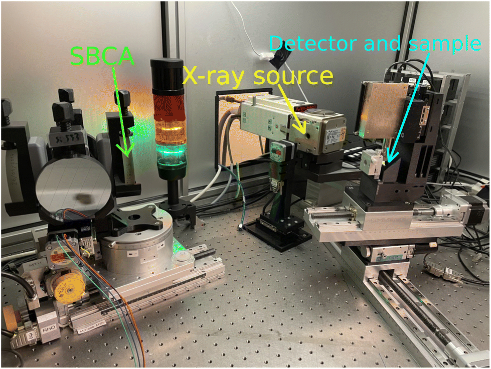 | ||
| Fig. 1 The HelXAS Johann-type spectrometer, consisting of an X-ray source, a four-crystal SBCA unit, a detector, motorized movement stages, a slit, and a sample stage. | ||
2.2. Fluorescence mode
When measuring the relevant X-ray fluorescence line yield while tuning the photon energy around the corresponding absorption edge, the intensity of the fluorescence line is approximately proportional to the absorption cross section. This holds in the limit of dilute and/or thin samples, when the self-absorption saturation effects can be assumed to be small, or at least small enough so that they can be corrected for in the data processing stage. To maximise the signal-to-noise ratio, the detector of the fluorescence radiation should cover as large solid angle as possible while not being saturated, sometimes with specific filters to reduce possible undesired spectral lines. To minimize the background from Compton and elastic scattering, a typical experimental setup at a synchrotron light source with linearly polarized light utilizes a 90° scattering angle in the plane of the synchrotron orbit. In this geometry, the Thomson scattering cross section is minimized owing to the dot product of the polarization vectors of the incoming (ε1) and of the scattered (ε2) light:r0 being the electron classical radius. This geometry typically maximises the signal-to-noise ratio in fluorescence detection mode. The radiation from a conventional X-ray tube is not polarized, but a 90° scattering geometry for the fluorescencedetection is nevertheless desirable since it will still help to reduce the Thomson scattering cross section by a factor of two. For unpolarized radiation, the Thomson scattering cross section is
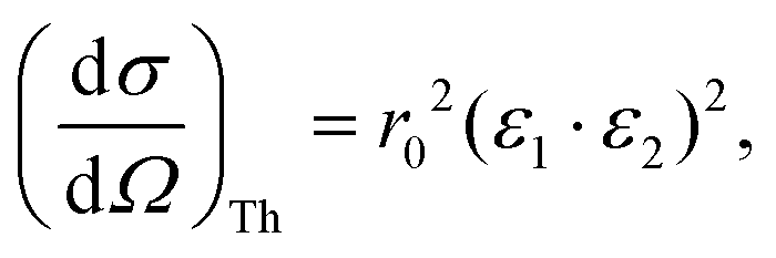
and when the scattering angle 2θ = 90°, this contribution is at its minimum. Considering the Thomson scattering cross section only, there is no preference for vertical or horizontal placement of the detector with respect to the sample, and we have chosen to use the vertical geometry, since it minimizes the footprint of the detector assembly in the experimental setup.
The incoming X-ray beam from the monochromator should be in as grazing incidence as possible with respect to the sample surface. The relatively large beam spot on the sample from a conventional X-ray tube and SBCA optics does not permit very small grazing incidence angles, but we have found that a 10 degree angle between the X-ray beam and the sample surface is a good compromise between maximising the signal and facilitating the alignment. This is coupled to a specific feature of the focusing capability of an SBCA. It does not offer perfect point-to-point focal image of the source on the sample position, owing to the spherical astigmatism that results in two spatially separated line foci when the Bragg angle is below 90°. The foci are located at distances R![[thin space (1/6-em)]](https://www.rsc.org/images/entities/char_2009.gif) sinθB and R/sinθB from the monochromator. The closest focus is located on the Rowland circle and provides focusing in the dispersive direction, while the latter is located outside the Rowland circle and provides focusing in the nondispersive direction. In our case, the Rowland circle is horizontal, and thus the nominal focus at RsinθB resembles a vertically extended line. The most common sample location in such a Rowland-circle instrument would be at this focal position. However, in order to illuminate the sample in the most optimal way in the geometry where the detector is placed above the sample, we have opted to use the secondary line focus outside the Rowland circle, in this case vertically focused but horizontally extended. When the sample is placed in the location of this line focus, in a grazing incidence geometry the beam footprint on the sample surface has a rectangular shape, a few millimeters in each dimension depending on the exact Bragg angle. That is the optimal footprint to conform with samples that are most typically cut into an approximately rectangular shape as is the case in this study.
sinθB and R/sinθB from the monochromator. The closest focus is located on the Rowland circle and provides focusing in the dispersive direction, while the latter is located outside the Rowland circle and provides focusing in the nondispersive direction. In our case, the Rowland circle is horizontal, and thus the nominal focus at RsinθB resembles a vertically extended line. The most common sample location in such a Rowland-circle instrument would be at this focal position. However, in order to illuminate the sample in the most optimal way in the geometry where the detector is placed above the sample, we have opted to use the secondary line focus outside the Rowland circle, in this case vertically focused but horizontally extended. When the sample is placed in the location of this line focus, in a grazing incidence geometry the beam footprint on the sample surface has a rectangular shape, a few millimeters in each dimension depending on the exact Bragg angle. That is the optimal footprint to conform with samples that are most typically cut into an approximately rectangular shape as is the case in this study.
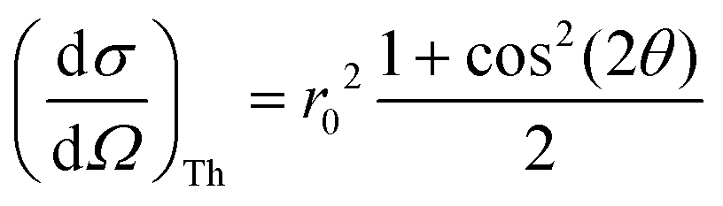
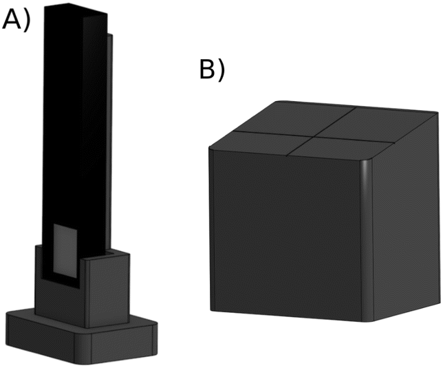
To realize this design, we have manufactured by 3D-printing a dedicated sample-detector assembly, shown in Fig. 2. For a possibility to shape the beam if necessary, a slit (Huber GmbH slit screen 3002.10) is fixed to the base. The SDD detector distance from the sample can be adjusted with a manual micrometer screw, and the sample support is a separate solid piece attached to the base with magnets for easy sample replacement. The adjustment can also be used to find optimal signal without saturating the detector. It should be mentioned that while the detector saturation may be an issue at a synchrotron light source, using low-brilliance X-ray sources we have not found such effects in fluorescence mode thin film research yet. Hence the detector can usually be brought as close to the sample as possible as long as it does not touch the sample or block the incident beam, i.e., typically at a 1–2 mm distance from the sample's surface. The computer aided designs of 3D printed parts are available online (https://tinyurl.com/fluorescenceMode).
 | ||
| Fig. 2 The fluorescence mode setup for measuring thin films, consisting of a base, slit, sample support, detector, and an adjustable arm for the detector. | ||
θB from the SBCA. The sample support for the near grazing incidence (10°) (Fig. 3b) allows a precise placement of the sample on the beam as aligned with the PSD. Both of the parts use a fixation to the base using magnets. The drawings are specific to the components listed in the ESI,† but adoption to other devices with similar functionality is straightforward.
 | ||
| Fig. 3 The two pieces for alignment: (A) vertical support for the Minipix-detector, (B) support for the sample where the sample positioning is at 10° angle. The sample will be centered at the crosshair position. | ||
Fig. 4 shows the image of the incident beam as seen by the PSD, at the alignment for incident photon energy of 9.0 keV (Bragg angle 77° with the Si(553) SBCA). From this image we can estimate the beam size to be 0.6 mm (height) × 6 mm (width). When projected to a sample in a 10° incidence angle, it will illuminate an area that is 6 mm wide and 0.6 mm/sin(10°) ≈ 3.5 mm in height. Fig. 5 illustrates the illumination of the sample with such a beam when the sample is placed on the support.
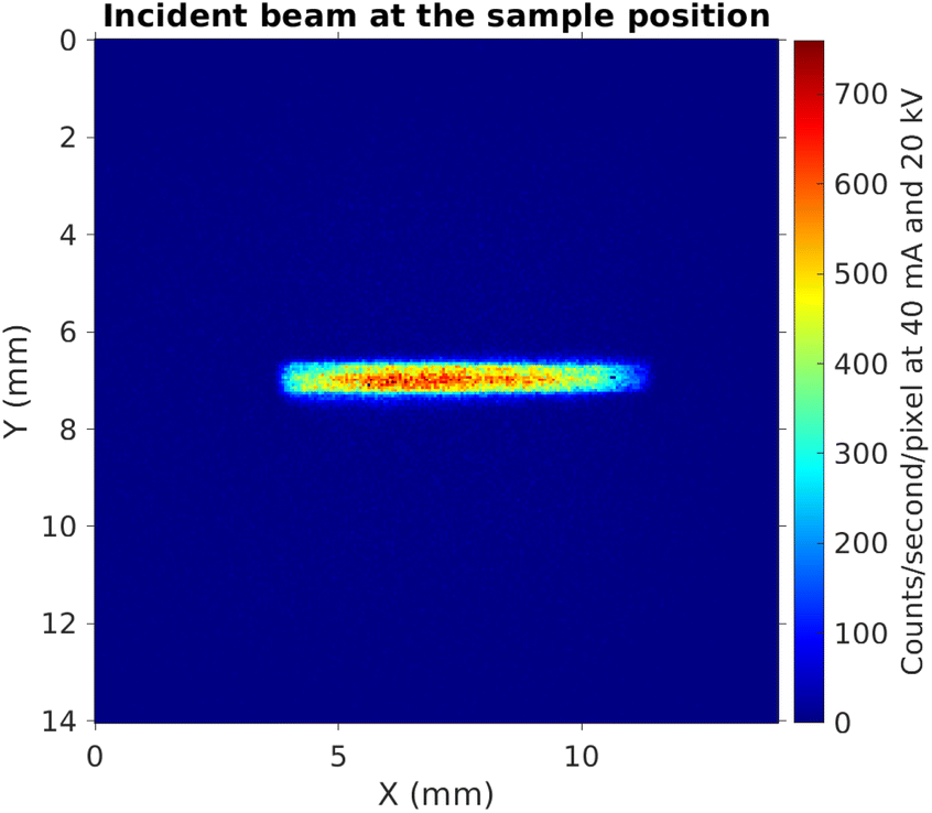 | ||
| Fig. 4 The incident beam at the nominal sample position (without tilt). | ||
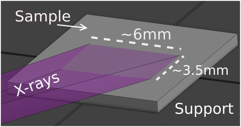 | ||
| Fig. 5 An illustration of the illumination of the sample with horizontal on focused beam. | ||
2.3. In situ annealing setup
For in situ annealing, the sample was kept in the same position and orientation as in the ex situ measurements, while being mounted on a metal-ceramic heater. For this purpose we designed another 3D-printed support. The support was printed using poly(lactic acid) (PLA) filament. We used a 24 W heater with a 20 × 20 mm2 surface, and placed a thermocouple on the heater in order to monitor the temperature. The setup is shown in Fig. 6. The conducting metal wires from the heater were covered with polytetrafluoroethylene (PTFE) tube to insulate the PLA support, which has a glass transition temperature around 60 °C.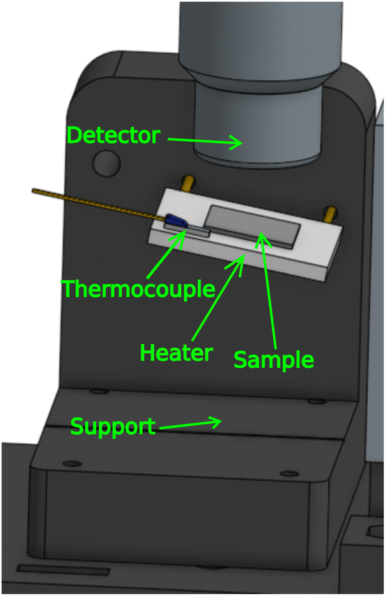 | ||
| Fig. 6 An illustration of sample annealing setup. | ||
2.4. Samples and sample preparation
Samples used in our measurements were provided by HelsinkiALD group (https://www.helsinki.fi/en/researchgroups/helsinkiald). They consisted of copper iodide (CuI) thin films with 248 nm, 244 nm, 160 nm, 119 nm, 34 nm, and 28 nm thicknesses along with copper oxide films with 144 nm, 93 nm, 71 nm, 50 nm, 25 nm, and 12 nm thicknesses. CuI thin films were deposited via gas phase conversion from CuO thin films made by ALD.37 In short, ALD CuO thin films were deposited according to Iivonen et al.,38 using bis(dimethylamino-2-propoxy) copper(II) (Cu(dmap)2) and ozone (O3) as precursors.Gas phase conversions were performed with hydroiodic acid at room temperature under reduced pressure (<1 mbar) and yielded phase-pure CuI thin films. Films were grown on oxide covered silicon substrates and samples were cut into approximately 10 mm × 10 mm sized plates. CuI film thicknesses were determined from energy-dispersive X-ray spectroscopy (EDS) data measured using Oxford INCA 350 microanalysis system connected to a Hitachi S-4800 field-emission scanning electron microscope (FESEM). The thicknesses were calculated from the EDS data with GMRFilm software39 using bulk density of CuI (5.67 g cm−3). Element concentrations were calculated from the EDS data using the intensities of I Lα and Cu Kα lines.
As a reference we used CuI powder (Sigma Aldrich, 215554-5G, 99.999% trace metals basis), ∼15 mg of CuI was mixed with ∼100 mg of potato starch buffer material and pressed to a pellet. The XAS measurement of this reference pellet was done in transmission mode. Another reference sample was 12.5 μm thick Cu metal foil acquired from Goodfellow Inc., measured both in transmission and fluorescence mode. The energy calibration was done so that the energy of the first peak of the first derivative of the metal foil spectrum was set to 8.979 keV.
2.5. Data analysis
Fig. 7 shows a typical set of multichannel analyser (MCA) spectra as a function of incident photon energy. A selected single spectrum, taken at the incident photon energy 8.999 keV, marked with the red dashed line, is shown separately. The spectrum consists of the emission lines from copper and iodine in the thin film; Ag, Fe, and Ni lines from the X-ray source and spectrometer components; Si Kα1,2 line from the substrate; and elastic and Compton scattering. The Cu Kα1,2 line is highlighted as the region of interest (ROI) with red dashed lines. The energy axis was calibrated using an Am-241 source.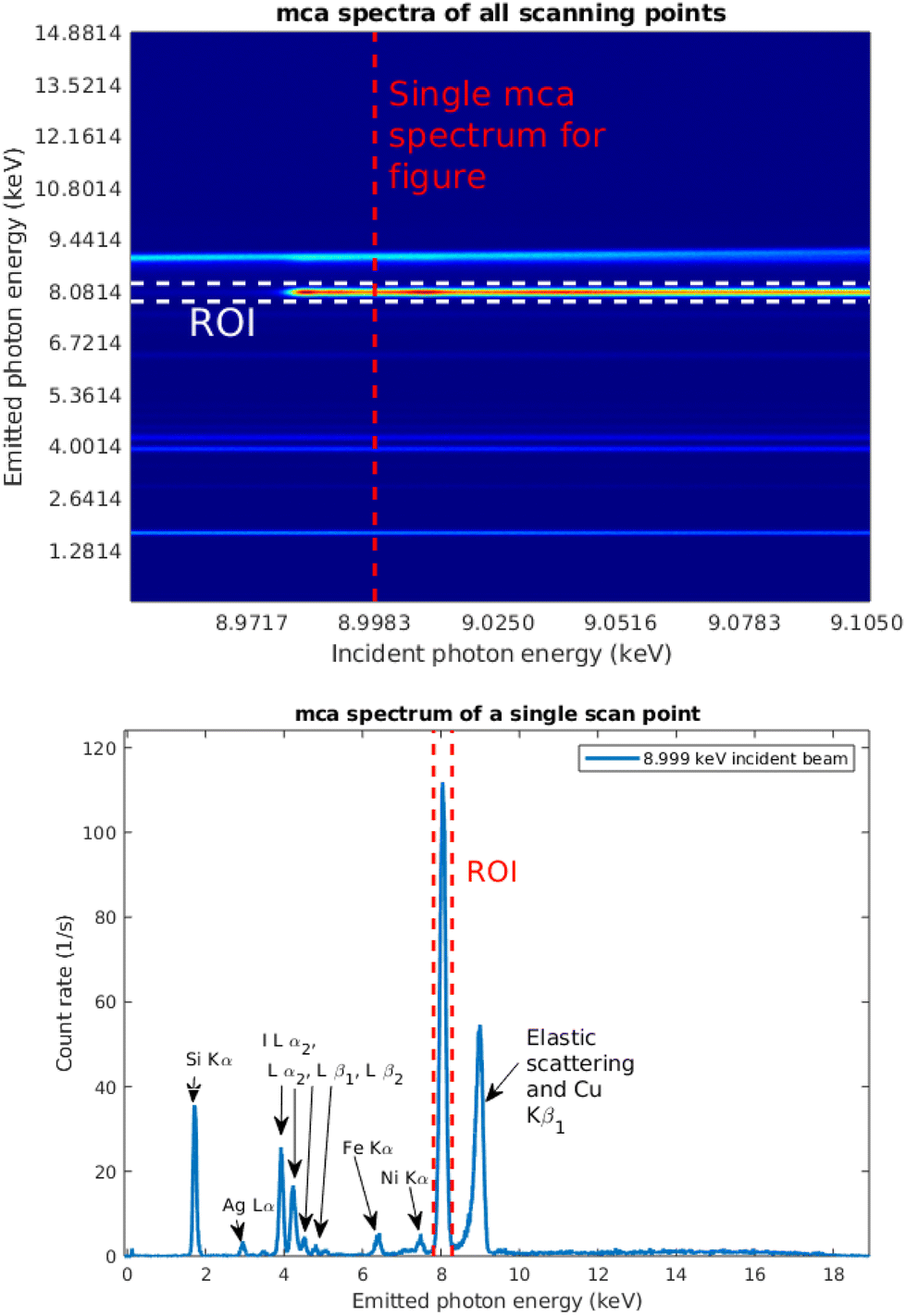 | ||
| Fig. 7 Top panel: 2D plot of signal per bin at each scan point for energy scan between 8.93–8.97 keV where the ROI of the signal is highlighted between bin numbers 1160 and 1230. The scan from which figure is taken is highlighted with a red dashed line. Bottom panel: an MCA spectrum of a CuI sample at 9.0 keV where the Cu Kα1,2 region is highlighted with red dashed lines. This region was selected as the ROI for the data analysis. The other features of the spectrum are identified as well. | ||
For the data analysis, in addition to the relevant fluorescence signal If, a measurement of a signal that is proportional to the intensity of the incident beam I0 needs to be obtained. The absorption spectrum is then obtained from μ = If/I0. In the previous work,19 the reference signal for a sample containing element Z of interest, the fluorescence from a Z − 1 foil was used, which required two different measurements. In this case we utilized the Si Kα fluorescence line intensity as the reference signal.
The references that were measured in transmission mode, were treated in the following way. The transmitted intensity through a sample (I) was measured with the SDD behind the sample, and the incident beam intensity I0 was measured without the sample. Absorbance μ(E) was obtained from Beer–Lambert's law: μ = log(I0/I). Linear background was fitted to the pre-edge region and the XANES spectra obtained this way were normalized to unit area. The EXAFS spectrum was analyzed using Larch XAS analysis package.40
3. Results
3.1. XANES
| Sample | Count rate at peak | Background |
|---|---|---|
| CuI 248 nm | 3700 s−1 | ∼45 s−1 |
| CuI 244 nm | 3500 s−1 | ∼45 s−1 |
| CuI 160 nm | 2400 s−1 | ∼35 s−1 |
| CuI 119 nm | 2000 s−1 | ∼30 s−1 |
| CuI 34 nm | 600 s−1 | ∼15 s−1 |
| CuI 28 nm | 430 s−1 | ∼15 s−1 |
| CuO 144 nm | 5100 s−1 | ∼60 s−1 |
| CuO 93 nm | 4100 s−1 | ∼50 s−1 |
| CuO 71 nm | 2500 s−1 | ∼32 s−1 |
| CuO 50 nm | 1900 s−1 | ∼30 s−1 |
| CuO 25 nm | 1100 s−1 | ∼20 s−1 |
| CuO 12 nm | 500 s−1 | ∼12 s−1 |
The measured raw spectra in units of measured Cu Kα1,2 fluorescence line intensity are shown in Fig. 8. As expected, the intensity is roughly proportional to the film thickness. Assuming that the fluorescence intensity is linearly proportional to the absorption cross-section μ(E), from the raw spectra of Fig. 8 the data were processed by subtracting a constant to represent the pre-edge background, and normalizing the spectra to a unit area. The resulting spectra of thin films and references are shown in Fig. 9 and 10 for CuI and CuO samples respectively. The thin film samples exhibit spectra that match those of the references.
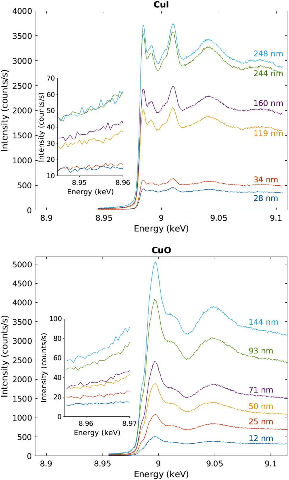 | ||
| Fig. 8 Raw data in units of counts per second recorded by the fluorescence detector. The inset shows a close-up to the pre-edge background, CuI samples above and CuO below. | ||
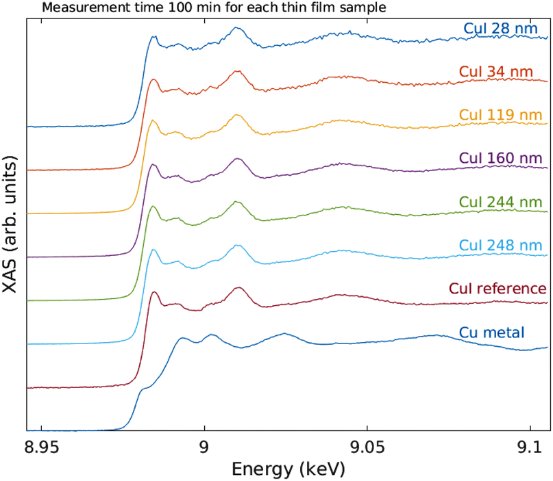 | ||
| Fig. 9 XANES spectra of the Cu K edge of the CuI thin films and references. | ||
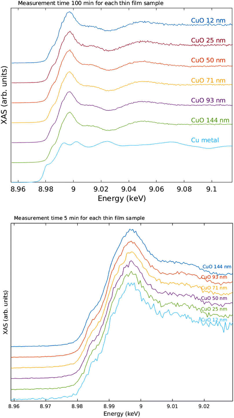 | ||
| Fig. 10 XANES spectra of the Cu K edge of the CuO thin films and references. Top: 100 min measurement time per sample, bottom: 5 min per sample. | ||
As a precaution to reduce the heat load on the detector, the detector-sample distance was increased to 8 mm and the detector head was covered with a Kapton foil. These changes reduced the count rate from 3700 s−1 to ∼660 s−1 on the maximum of the white line of the Cu K edge, mostly due to the smaller captured solid angle.
The sample temperature was first set to ∼220 °C, at which stage an initial spectrum was acquired. Then, the following cycle was repeated until the sample was fully oxidized: (1) the temperature was increased to 245° for 1 min, and decreased back to 220°, after which (2) the Cu K edge XANES was measured. The results from in situ annealing experiment along with reference spectra of bulk CuI and CuO are shown in Fig. 11.
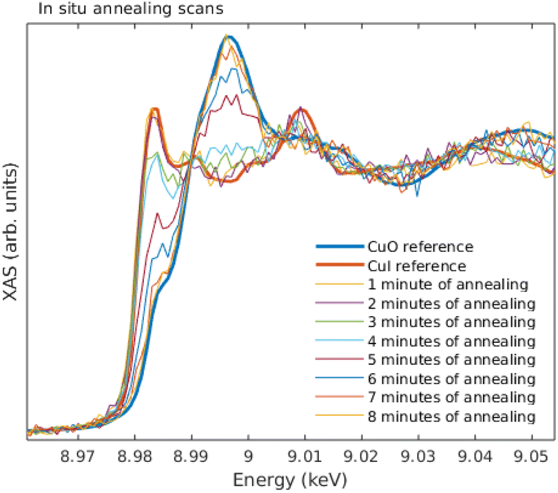 | ||
| Fig. 11 In situ measurement of annealing CuI film in 245 °C, along the reference spectra of CuI and CuO standards. | ||
3.2. EXAFS of CuI
EXAFS spectra were obtained from the 28 nm and 248 nm thick CuI samples. First, the near-edge region was measured in energy space between 8.9 keV and 9.0 keV in 100 scan points with 0.5 eV spacing. The actual EXAFS region was measured in k-space between 0 and 11 Å−1 with 180 scan points, equidistant in k-space, with 10 s measurement time per point in both scanning ranges. The measured spectra were then concatenated into a single spectrum and analyzed using the Larch software.40 The total time used for the EXAFS measurements were 47 and 94 hours for 248 nm and 28 nm thick samples, respectively.As can be seen from Fig. 12, obviously the EXAFS spectra in k-space exhibit noise at large values of the photoelectron momentum k, but useful data can be obtained up to about 10 Å−1 in this experiment. The Fourier-transformed EXAFS spectrum in R-space gives identical results for the 28 nm and 248 nm samples.
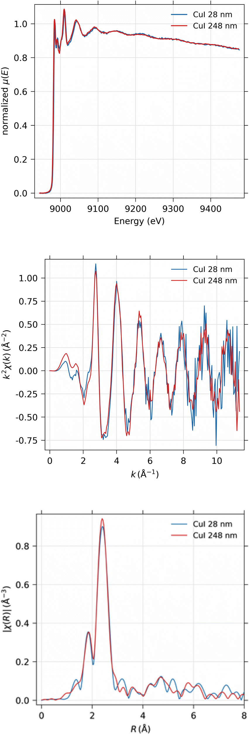 | ||
| Fig. 12 From top to bottom: the measured XAS of CuI thin films with 28 nm and 248 nm thickness for EXAFS analysis; EXAFS spectrum χ(k)k2 in k-space; Fourier-transformed EXAFS spectrum χ(r) in real space. | ||
The EXAFS spectrum was modelled using FEFF 8.5 software41 with the CuI zinc blende crystal structure42 by fitting only the first shell since there is only one notable peak in the Fourier-transformed spectrum. The modelled spectrum is compared with 248 nm CuI sample χ(k)k2 and Fourier-transformed EXAFS spectrum χ(r) in Fig. 13. In a similar fashion, the comparison of fitted and measured spectra for 28 nm are shown in Fig. 14. The obtained values for S02, δE0, R, and σ2 are tabulated for both 248 nm and 28 nm in Table 2.
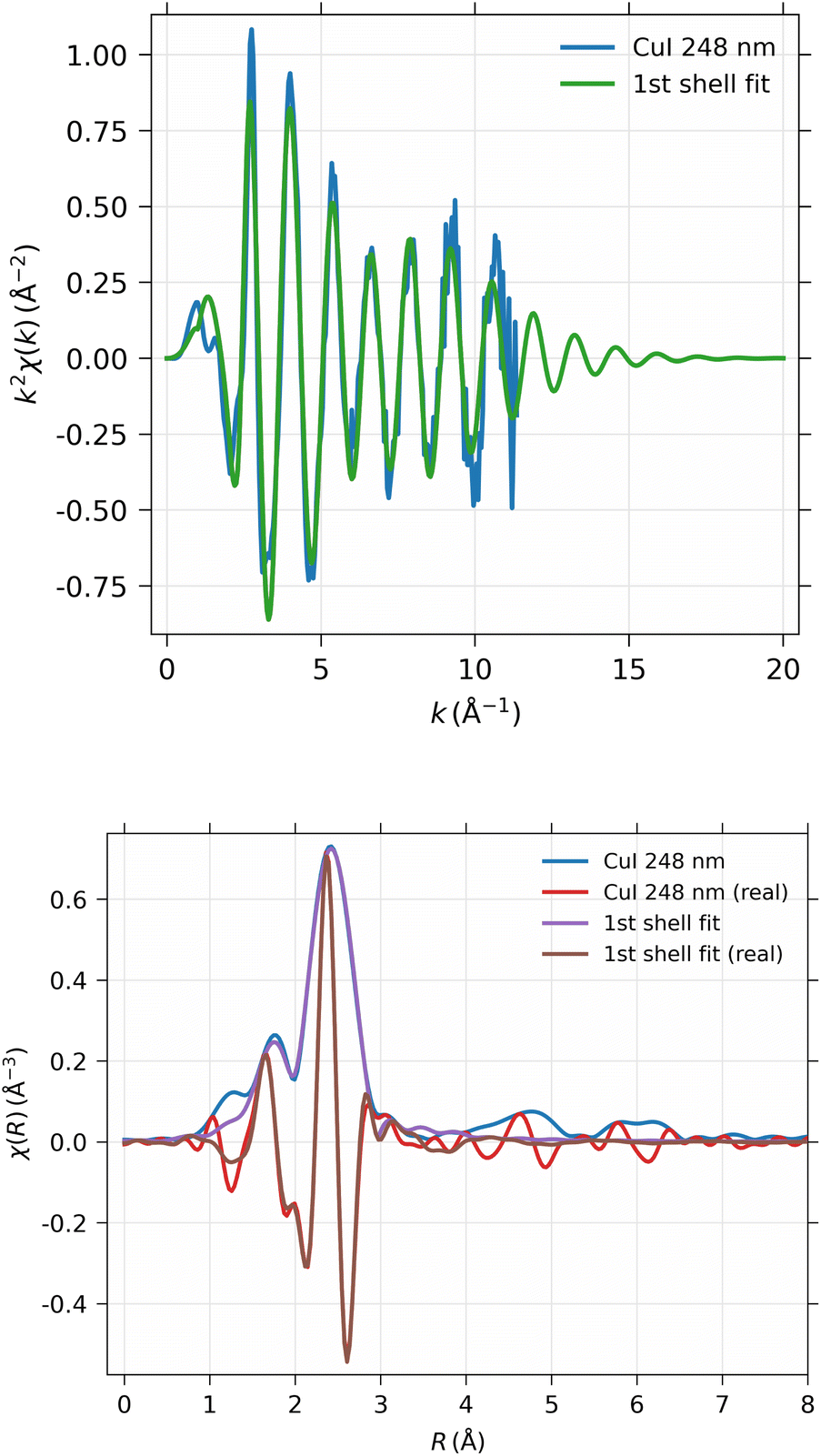 | ||
| Fig. 13 EXAFS spectra simulated with FEFF, compared with the experimental results from the 248 nm thick CuI film. Top panel: EXAFS spectrum χ(k)k2 in k-space; bottom panel: Fourier-transformed EXAFS spectrum χ(R). | ||
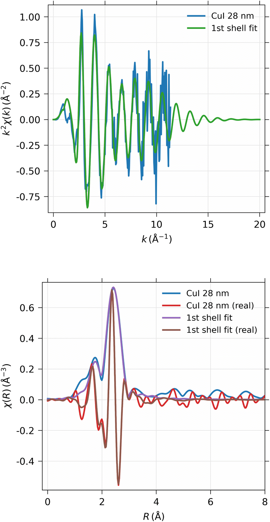 | ||
| Fig. 14 EXAFS spectra simulated with FEFF, compared with the experimental results from the CuI 28 nm sample. Top panel: EXAFS spectrum χ(k)k2 in k-space; bottom panel: Fourier-transformed EXAFS spectrum χ(R). | ||
| CuI 244 nm | CuI 28 nm | |
|---|---|---|
| S 0 2 | 0.747 ± 0.020 | 0.742 ± 0.031 |
| ΔE0 | 3.87 ± 0.24 eV | 3.85 ± 0.35 eV |
| R | 2.622 ± 0.0022 Å | 2.618 ± 0.0033 Å |
| σ 2 | 0.01002 ± 0.00032 Å2 | 0.00980 ± 0.00046 Å2 |
| R-factor | 0.144 | 0.146 |
4. Discussion
Overall, the quality of the spectra could easily be used in typical XANES analysis even from the thinnest films measured here. The data acquisition times for a decent ex situ XANES spectrum range in 5–20 minutes. In the in situ annealing experiment we demonstrated through a simple example how the methods developed and described in this article can be used to track the changes of the oxidation state and local chemical environment. The substantial increase, roughly 300 times, in photon counts when comparing with previous demonstration19 also enabled EXAFS measurements. The data acquisition times for EXAFS measurements range between 1–4 days.From the ex situ XANES and EXAFS spectra we could confirm that there were no detectable changes in the chemical state as a function of thickness for both CuI and CuO samples, i.e., the sample preparation method produced the wanted thin film regardless of the thickness of the sample. From in situ annealing XANES spectra we see a clear conversion of CuI back to CuO as a function of annealing time. At the end of the annealing, all of the CuI had converted to CuO.
Our results show clearly that routine XANES and EXAFS characterization of thin films can be done by using laboratory-scale instruments, including in situ experiments for slow chemical reactions with a minute-scale time resolution. Naturally, for faster reactions high-brilliance sources such as synchrotrons remain the tool of choice. Nevertheless, even in those cases, the laboratory-scale XAS instruments can be e.g., used for preliminary studies to strengthen a beamtime application and for training of users before an actual beamtime, as comprehensively presented in ref. 18.
5. Conclusions
In this article we have described an optimized setup to measure thin films in fluorescence mode with a laboratory-scale XAS spectrometer. The quality of the data that can be obtained with the setup is demonstrated with Cu K-edge XANES and EXAFS measurements with a set of CuI and CuO thin films with 12–248 nm thicknesses. The presented methods show that XAS studies of thin films are possible using laboratory-scale spectrometers and can e.g., address the need when doing rapid prototyping, and we see great potential for laboratory-scale XAS as a routine characterisation tool for thin film research. Possible future in situ and operando studies, e.g., during film growth, can be considered with the high data quality from the ex situ experiments demonstrated here.Conflicts of interest
There are no conflicts to declare.Acknowledgements
A.-J. K. was supported by the University of Helsinki Doctoral Program in Materials Research and Nanosciences (MATRENA). The authors thank the Academy of Finland (decision numbers 295696 and 330086). The authors thank the Helsinki Center for X-ray Spectroscopy for beamtime at the HelXAS instrument under the proposal 2022-0010. The use of ALD Center Finland research infrastructure is acknowledged.References
- J. M. P. Alaboson, Q. H. Wang, J. D. Emery, A. L. Lipson, M. J. Bedzyk, J. W. Elam, M. J. Pellin and M. C. Hersam, ACS Nano, 2011, 5, 5223–5232 CrossRef CAS PubMed.
- S. Sofia, J. Mailoa, D. Weiss, B. Stanbery, T. Buonassisi and I. M. Peters, Nat. Energy, 2018, 3, 387–394 CrossRef.
- Z. Yu, J. Carpenter and Z. Holman, Nat. Energy, 2018, 3, 747–753 CrossRef CAS.
- B. J. O'Neill, D. H. K. Jackson, J. Lee, C. Canlas, P. C. Stair, C. L. Marshall, J. W. Elam, T. F. Kuech, J. A. Dumesic and G. W. Huber, ACS Catal., 2015, 5, 1804–1825 CrossRef.
- J. Gambetta, J. Chow and M. Steffen, npj Quantum Inf., 2017, 3, 2 CrossRef.
- M. Leskelä and M. Ritala, Angew. Chem., Int. Ed., 2003, 42, 5548–5554 CrossRef PubMed.
- S. M. George, Chem. Rev., 2010, 110, 111–131 CrossRef CAS PubMed.
- R. Johnson, A. Hultqvist and S. Bent, Mater. Today, 2014, 17, 236–246 CrossRef CAS.
- O. Trejo, K. E. Roelofs, S. Xu, M. Logar, R. Sarangi, D. Nordlund, A. L. Dadlani, R. Kravec, N. P. Dasgupta, S. F. Bent and F. B. Prinz, Nano Lett., 2015, 15, 7829–7836 CrossRef CAS PubMed.
- A. Dadlani, O. Trejo, S. Acharya, J. Torgersen, I. Petousis, D. Nordlund, R. Sarangi, P. Schindler and F. Prinz, J. Mater. Chem. C, 2015, 3, 12192–12198 RSC.
- A. Dadlani, S. Acharya, O. Trejo, F. Prinz and J. Torgersen, ACS Appl. Mater. Interfaces, 2016, 8, 14323–14327 CrossRef CAS PubMed.
- M. Filez, E. A. Redekop, J. Dendooven, R. K. Ramachandran, E. Solano, U. Olsbye, B. M. Weckhuysen, V. V. Galvita, H. Poelman, C. Detavernier and G. B. Marin, Angew. Chem., Int. Ed., 2019, 58, 13220–13230 CrossRef CAS PubMed.
- F. Meirer and B. M. Weckhuysen, Nat. Rev. Mater., 2018, 3, 324–340 CrossRef.
- O. Trejo, A. L. Dadlani, F. De La Paz, S. Acharya, R. Kravec, D. Nordlund, R. Sarangi, F. B. Prinz, J. Torgersen and N. P. Dasgupta, Chem. Mater., 2019, 31, 8937–8947 CrossRef CAS.
- X. Qu, D. Yan, R. Li, J. Cen, C. Zhou, W. Zhang, D. Lu, K. Attenkofer, D. J. Stacchiola, M. S. Hybertsen, E. Stavitski and M. Liu, Chem. Mater., 2021, 33, 1740–1751 CrossRef CAS.
- A. Wise, C. Ban, J. Weker, S. Misra, A. Cavanagh, Z. Wu, Z. Li, M. Whittingham, K. Xu, S. George and M. Toney, Chem. Mater., 2015, 27, 6146–6154 CrossRef CAS.
- G. T. Seidler, D. R. Mortensen, A. J. Remesnik, J. I. Pacold, N. A. Ball, N. Barry, M. Styczinski and O. R. Hoidn, Rev. Sci. Instrum., 2014, 85, 113906 CrossRef CAS PubMed.
- A. S. Ditter, E. P. Jahrman, L. R. Bradshaw, X. Xia, P. J. Pauzauskie and G. T. Seidler, J. Synchrotron Radiat., 2019, 26, 2086–2093 CrossRef CAS PubMed.
- A.-P. Honkanen, S. Ollikkala, T. Ahopelto, A.-J. Kallio, M. Blomberg and S. Huotari, Rev. Sci. Instrum., 2019, 90, 033107 CrossRef PubMed.
- Z. Németh, J. Szlachetko, E. Bajnoczi and G. Vankó, Rev. Sci. Instrum., 2016, 87, 103105 CrossRef PubMed.
- J. Hoszowska, J.-C. Dousse, J. Kern and C. Rhême, Nucl. Instrum. Methods Phys. Res., Sect. A, 1996, 376, 129–138 CrossRef CAS.
- H. Legall, H. Stiel, M. Schnürer, M. Pagels, B. Kanngießer, M. Müller, B. Beckhoff, I. Grigorieva, A. Antonov, V. Arkadiev and A. Bjeoumikhov, J. Appl. Crystallogr., 2009, 42, 572–579 CrossRef CAS.
- L. Anklamm, C. Schlesiger, W. Malzer, D. Grötzsch, M. Neitzel and B. Kanngießer, Rev. Sci. Instrum., 2014, 85, 053110 CrossRef PubMed.
- L. C. Jarrott, M. S. Wei, C. McGuffey, F. N. Beg, P. M. Nilson, C. Sorce, C. Stoeckl, W. Theoboald, H. Sawada, R. B. Stephens, P. K. Patel, H. S. McLean, O. L. Landen, S. H. Glenzer and T. Döppner, Rev. Sci. Instrum., 2017, 88, 043110 CrossRef CAS PubMed.
- M. Kavčič, M. Budnar, A. Mühleisen, F. Gasser, M. Žitnik, K. Bučar and R. Bohinc, Rev. Sci. Instrum., 2012, 83, 033113 CrossRef PubMed.
- J. Holburg, M. Müller, K. Mann, P. Wild, K. Eusterhues and J. Thieme, Anal. Chem., 2022, 94, 3510–3516 CrossRef CAS PubMed.
- B. Buades, A. Picón, E. Berger, I. León, N. Di Palo, S. L. Cousin, C. Cocchi, E. Pellegrin, J. H. Martin, S. Mañas-Valero, E. Coronado, T. Danz, C. Draxl, M. Uemoto, K. Yabana, M. Schultze, S. Wall, M. Zürch and J. Biegert, Appl. Phys. Rev., 2021, 8, 011408 CAS.
- E. P. Jahrman, L. A. Pellerin, A. S. Ditter, L. R. Bradshaw, T. T. Fister, B. J. Polzin, S. E. Trask, A. R. Dunlop and G. T. Seidler, J. Electrochem. Soc., 2019, 166, A2549–A2555 CrossRef CAS.
- K. Lahtinen, M. Labmayr, V. Mäkelä, H. Jiang, J. Lahtinen, L. Yao, E. O. Fedorovskaya, S. Räsänen, S. Huotari and T. Kallio, Mater. Today Energy, 2022, 101040 CrossRef CAS.
- J. Moya-Cancino, ChemCatChem, 2019, 11, 1039–1044 CrossRef CAS PubMed.
- N. S. Genz, A.-J. Kallio, R. Oord, F. Krumeich, A. Pokle, Ø. Prytz, U. Olsbye, F. Meirer, S. Huotari and B. M. Weckhuysen, Angew. Chem., Int. Ed., 2022, e202209334 CAS.
- W. Malzer, D. Grötzsch, R. Gnewkow, C. Schlesiger, F. Kowalewski, B. Van Kuiken, S. DeBeer and B. Kanngießer, Rev. Sci. Instrum., 2018, 89, 113111 CrossRef PubMed.
- R. Bès, T. Ahopelto, A.-P. Honkanen, S. Huotari, G. Leinders, J. Pakarinen and K. Kvashnina, J. Nucl. Mater., 2018, 507, 50–53 CrossRef.
- P. Zimmermann, S. Peredkov, P. M. Abdala, S. DeBeer, M. Tromp, C. Müller and J. A. van Bokhoven, Coord. Chem. Rev., 2020, 423, 213466 CrossRef CAS.
- W. Malzer, C. Schlesiger and B. Kanngießer, Spectrochim. Acta, Part B, 2021, 177, 106101 CrossRef CAS.
- M. Rovezzi, C. Lapras, A. Manceau, P. Glatzel and R. Verbeni, Rev. Sci. Instrum., 2017, 88, 013108 CrossRef PubMed.
- A. Weiß, J. Goldmann, S. Kettunen, G. Popov, T. Iivonen, M. Mattinen, P. Jalkanen, T. Hatanpää, M. Leskelä, M. Ritala and M. Kemell, Adv. Mater. Interfaces, 2022 DOI:10.1002/admi.202201860 , manuscript accepted.
- T. Iivonen, J. Hämäläinen, B. Marchand, K. Mizohata, M. Mattinen, G. Popov, J. Kim, R. A. Fischer and M. Leskelä, J. Vac. Sci. Technol., A, 2016, 34, 01A109 CrossRef.
- R. Waldo, Proceedings of the 23rd Annual Conference of the Microbeam Analysis Society, 1988, p. 310 Search PubMed.
- M. Newville, J. Phys.: Conf. Ser., 2013, 430, 012007 CrossRef CAS.
- J. J. Rehr, J. J. Kas, F. D. Vila, M. P. Prange and K. Jorissen, Phys. Chem. Chem. Phys., 2010, 12, 5503–5513 RSC.
- J. Zemann, Acta Crystallogr., 1965, 18, 139–139 CrossRef.
Footnote |
| † Electronic supplementary information (ESI) available. See DOI: https://doi.org/10.1039/d2dt02264h |
| This journal is © The Royal Society of Chemistry 2022 |