
 Open Access Article
 This Open Access Article is licensed under a Creative Commons Attribution-Non Commercial 3.0 Unported Licence
A highly hydroxylated 6-tin oxide cluster serves as an efficient e-beam and EUV-photoresist to achieve high-resolution patterns†
Cheng-Dun
Li
a,
Chun-Fu
Chou
a,
Yu-Fang
Tseng
a,
Burn-Jeng
Lin
*bc,
Tsai-Sheng
Gau
bc,
Po-Hsiung
Chen
bc,
Po-Wen
Chiu
bc,
Sun-Zen
Chen
d,
Shin-Lin
Tsai
e,
Wen-Bin
Jian
 e and
Jui-Hsiung
Liu
*ac
e and
Jui-Hsiung
Liu
*ac
aDepartment of Chemistry, National Tsing Hua University, Hsinchu, Taiwan
bTSMC-NTHU Joint Research Center, National Tsing Hua University, Hsinchu, Taiwan
cCollege of Semiconductor Research, National Tsing Hua University, Hsinchu, Taiwan
dCenter for Nanotechnology, Materials Science and Microsystem, National Tsing Hua University, Hsinchu, Taiwan
eDepartment of Electrophysics, National Yang Ming Chiao Tung University, Hsinchu, Taiwan. E-mail: rsliu@mx.nthu.edu.tw
First published on 21st January 2025
Abstract
A carboxylated-free cluster, formulated as (BuSn)6O4(OH)10 (2) was synthesized from the reaction of (BuSn)6O4Cl2(MeCO2)8 (1) with LiOH (aq.) in cold tetrahydrofuran (THF). This synthesis marks the first successful demonstration of complete decarboxylation of a metal carboxylate cluster using LiOH, resulting in the formation of a carboxylate-free metal oxide cluster. Comparative analysis of their 119Sn NMR, IR absorption spectra and ESI mass spectra suggests that cluster (2) possesses a ladder-type framework. Notably, cluster (2) exhibits superior surface smoothness and enhanced photosensitivity to both e-beams and EUV light compared to the well-known tin oxide cage, [(BuSn)12O14(OH)6](OH)2 (3). In e-beam lithography, cluster (2) facilitated the fabrication of high-resolution patterns with a half-pitch (HP) of 21 nm at a dose of J = 1760 μC cm−2. Similarly, its EUV lithography achieved an impressive HP of 16 nm at J = 70 mJ cm−2. In the etching resistance test, the tin carboxylate-free cluster (2) exhibited a low etching rate with a SiO2-selectivity contrast of approximately 1.53, which is significantly higher than the 0.73 observed for the model tin carboxylate cluster (1′). Mechanistic studies by both FTIR and HRXPS revealed that the extent of Sn–butyl loss is less significant than that of Sn–OH loss. The photolytic aggregation of cluster (2) predominantly involves the dehydration of two Sn–OH groups. Additionally, FTIR identified a surface reaction between SiOH and Sn–OH, forming new Sn–O–Si absorption peaks.
Introduction
Due to their strong absorption capabilities, metal-based photoresists have garnered significant interest in extreme ultraviolet (EUV) lithography.1–6 Achieving high-resolution patterns with small half-pitches (HP < 20 nm) is essential for producing integrated circuit (IC) chips at the sub-7 nm node. Metal clusters or nanoparticles are the materials of choice for photoresists owing to their high metal density. We7–10 and others11,12 reported several metal carboxylate clusters capable of achieving high-resolution patterns (HP < 20 nm) with low EUV doses (J < 60 mJ cm−2). Notably, metal carboxylate clusters typically exhibit low metal content, rendering them unsuitable for etching resistance tests.13 Following the development of lithographic patterns and a subsequent post-processing bake, a substantial proportion of metal oxide nanostructures is required to effectively etch the SiO2 layer. While SiO2-based nanostructures are highly sought in the IC industry, fabricating SiO2 patterns with small half-pitches (HP < 20 nm) requires exceptionally high EUV doses (>150 mJ cm−2) because of silicon's poor absorption ability.14,15 In contrast, tin oxide (SnO2) lithographic patterns can be readily achieved with low EUV energy doses, and their etching rates are relatively slow as compared to those of silicon nanostructures. Consequently, the development of SnO2-based nanostructures using EUV lithography represents a current trend in photoresist materials.To date, inorganic EUV photoresists have relied almost exclusively on metal oxide carboxylate clusters. However, carboxylate-free metal clusters, where carboxylate ligands are replaced by OH− or O2− ligands, are more desirable for IC applications due to their higher metal oxide content. Unfortunately, only one example such as 12-tin oxide cage, [(BuSn)12O14(OH)6](OH)2 (3),16–29 is known; this oxide cluster has attracted considerable interest due to its potential to form highly desirable SnO2-like nanostructures. In the edge etching process, the high SnO2 content of cluster (3) has been shown with a slow etching rate, enhancing its potential for commercial application.30 We seek a novel synthetic approach to access metal oxide clusters without any carboxylate ligand to achieve high SnO2 contents. This study reports the synthesis of a carboxylate-free hexameric tin oxide cluster, formulated as (BuSn)6O4(OH)10 (2), which is hypothesized to possess a ladder-type structure based on IR, 119Sn NMR, and ESI-mass (ESI = electron spray ionization) analyses. Notably, this new 6-tin cluster (2) demonstrates superior photosensitivity compared to the well-established 12-tin oxide cluster (3) under both e-beam and EUV exposure. Moreover, cluster (2) exhibits improved surface roughness relative to cluster (3). Using an e-beam energy source, a small half-pitch (HP = 21 nm) pattern was fabricated with a dose of 1760 μC cm−2, while a high-resolution pattern (HP = 16 nm) was achieved with an EUV dose of J = 56 mJ cm−2. Mechanistic studies of EUV-activated aggregation of the 6-tin cluster (2) were conducted by FTIR and HRXPS, which revealed that the primary mechanism involves dehydration of two Sn–OH groups, rather than the typical Sn–butyl bond cleavage.
We have recently developed a comprehensive strategy to enhance the performance of metal carboxylate clusters under EUV and e-beam conditions. Our findings indicate that substituting hydroxide for carboxylate ligands in these clusters not only achieves higher resolutions,7,8 but also reduces the required doses of e-beam or EUV exposure. For instance, a hafnium cluster, Hf6O4(OH)6(C4H9CO2)10, can achieve a HP = 16 nm pattern under EUV doses ranging from 170–180 mJ cm−2. Remarkably, a more hydroxylated cluster, Hf6(OH)8(C4H9CO2)8, is capable of fabricating the same HP = 16 nm pattern with significantly lower doses, between 90 and 100 mJ cm−2 to generate a large film thickness. Encouraged by this success, we are now extending this hydroxide substitution strategy to synthesize a new carboxylate-free tin oxide cluster (2) from a tin carboxylate cluster (1).
Etching resistance tests are completely absent in the existing literature on metal carboxylate clusters.1–5,7–12 It is crucial to establish a platform for assessing changes in etching performance when carboxylate ligands are replaced with hydroxides. In a previous study, we reported an efficient EUV photoresist, (vinylSn)6(sec-C4H9CO2)8O4Cl2 (1′), capable of achieving a HP of 16 nm with an exposure dose of J = 23 mJ cm−12. Here, we evaluate the photoresist performance of the carboxylate-free cluster (2) in comparison with the tin carboxylate cluster (1′). Notably, the tin carboxylate cluster (1′) exhibits inferior SiO2-selectivity (S = 0.73 versus S = 1.53 for (2)), possibly due to partial carboxylate decomposition under hard baking conditions.
Results and discussion
We previously reported the synthesis of hexameric tin carboxylate clusters (n-BuSn)6(MeCO2)8Cl2 (1),9 of which the structure has been characterized by X-ray diffraction study (CCDC 2019215). The ORTEP image and crystallographic studies are provided in the ESI.† This photoresist can achieve a high-resolution pattern (HP = 16 nm), albeit at a high EUV dose J = 200 mJ cm−2; the corresponding SEM images are provided in Fig. s2 (see the ESI).† We attempt to improve the EUV performance with hydroxide substitutions of chloro and acetate ligands. Apart from the small size, a Sn–OH group can serve as a coordinating ligand to fill an empty site around a Sn center during the EUV irradiation. As shown in Scheme 1, treatment of cluster (1) (300 mg) with 0.5 M LiOH (5 mL) in THF (20 mL) at 0 °C for 20 min yielded acetate-free white solid (2) in 23% yield. The new cluster (2) has a formula Sn6(n-butyl)6O4(OH)10. In elemental analysis, the carbon and hydrogen contents are found to be 22.92% and 4.77% respectively, very close to the calculated values: C, 23.01%, and H, 4.83%. In the 119Sn NMR spectra, three main peaks were observed at δ −450, −453, and −485 ppm, very close to those observed for the parent cluster (1), respectively at −467, −472, and −477 ppm. For the 12-tin oxide cluster (3), two 119Sn NMR peaks were reported at −280 and −463 ppm respectively. For this new cluster (2), there are small peaks at −244, −282, and −295 ppm that are approximately 10–13% in intensity as compared to those of the three main peaks. Such small tin signals arise possibly from the solution instability of cluster (2), which slowly forms the 12-tin-oxide cluster (3) at 25 °C. In a separate experiment, a THF solution of the fresh sample was allowed to stand at 25 °C for 48 h, and the resulting solution was analyzed to contain a mixture of clusters (2) and (3) in a 6![[thin space (1/6-em)]](https://www.rsc.org/images/entities/char_2009.gif) :1 ratio. These 119Sn NMR data and elemental analysis suggest that clusters (1) and (2) have similar ladder-type frameworks, with complete hydroxide substitution of two chloride and eight acetate ligands. We also conducted the powder X-ray diffraction analysis of cluster (2), with the absorption data presented in Fig. s1A.† The results show only a single minor peak within the 0° < 2θ < 60° range, indicating that cluster (2) is nearly completely amorphous. This structural characteristic makes the growth of single crystals of cluster (2) unattainable. To verify the postulated formula of Sn6(n-butyl)6O4(OH)10, ESI-mass spectra were recorded and are provided in Fig. s1B.† The calculated mass peak for the [12C241H6516O14120Sn6]+ cation is 1296.84423 whereas that of the observed peak is found to be 1296.85062. Additional mass peaks corresponding to different Sn isotopes are also observed as shown in Fig. s1B.†
:1 ratio. These 119Sn NMR data and elemental analysis suggest that clusters (1) and (2) have similar ladder-type frameworks, with complete hydroxide substitution of two chloride and eight acetate ligands. We also conducted the powder X-ray diffraction analysis of cluster (2), with the absorption data presented in Fig. s1A.† The results show only a single minor peak within the 0° < 2θ < 60° range, indicating that cluster (2) is nearly completely amorphous. This structural characteristic makes the growth of single crystals of cluster (2) unattainable. To verify the postulated formula of Sn6(n-butyl)6O4(OH)10, ESI-mass spectra were recorded and are provided in Fig. s1B.† The calculated mass peak for the [12C241H6516O14120Sn6]+ cation is 1296.84423 whereas that of the observed peak is found to be 1296.85062. Additional mass peaks corresponding to different Sn isotopes are also observed as shown in Fig. s1B.†
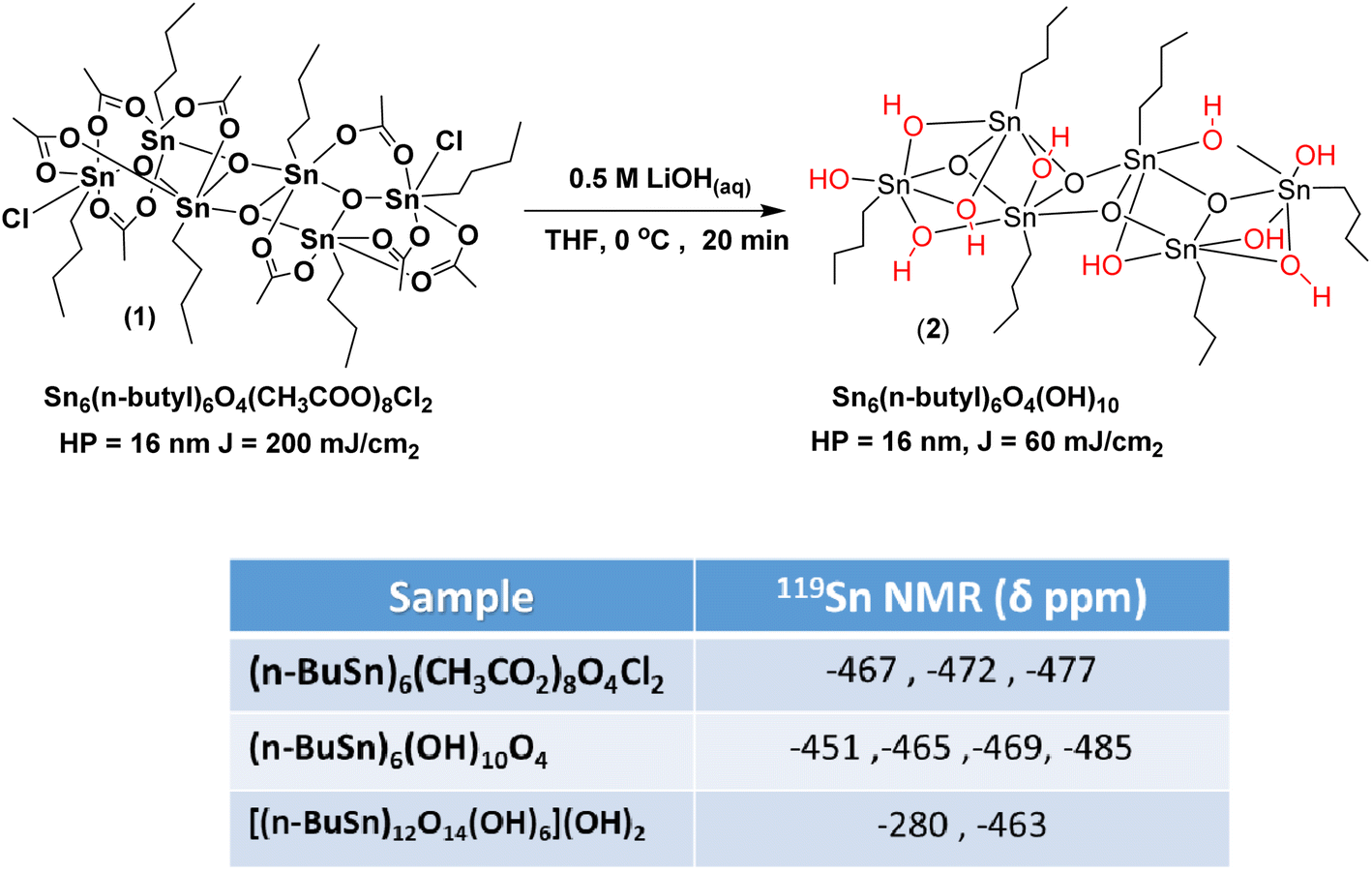 | ||
| Scheme 1 Synthesis of cluster (2) and a summary of 119Sn NMR data. | ||
Fig. 1 shows the thermal gravimetric (TGA) analysis of cluster (2) to test the rationales of our proposed formula. The proposed formula Sn6(n-butyl)6O4(OH)10 for cluster (2) is expected to form SnO2 after stepwise heating under an oxygen atmosphere. In the initial heating from 70 °C to 180 °C, a gradual loss of 6.5% weight is attributed to a dehydration reaction, corresponding to the reaction: 2Sn–OH → 2Sn2O + H2O. Notably, a complete loss of water for cluster (2) is calculated to be 7.0% very close to our observed data (6.5%). Herein, this dehydration is nearly complete at 180 °C. A second stage in the heating process (180–400 °C) mainly involves thermal Sn–butyl bond cleavage. A complete loss of the butyl group is expected to give an additional 26.6% weight loss, very close to our experimental data (24.0%). The residue remains at a constant weight (ca. 69.5%) after 410 °C, very close to the theoretical value of SnO2 formation (70%). This observation indicates negligible loss of volatile Sn species during the stepwise heating of cluster (2). In contrast, clusters (1) and (1′) gave low-weight residues, ca. 47.4% and 39.6%, much lower than the 54.4% and 49.7% values calculated for the SnO2 formation. The formation of SnClxO2−x/2 is also unlikely because of its high formula weight. Significant volatile tin species such as SnCl2 or SnCl4 are likely to occur for clusters (1) and (1′). Accordingly, cluster (2) outperforms clusters (1) and (1′) not only due to its high SnO2 content but also the absence of volatile Sn species. The low SnO2 contents of carboxylate clusters 1 and 1′ indicate their potential problems in edge etching resistance tests.
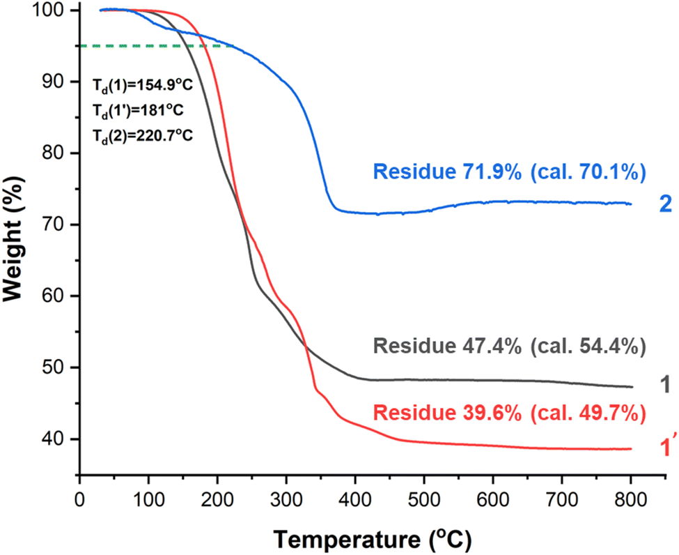 | ||
| Fig. 1 Thermal gravimetric analysis of clusters (1), (1′), and (2); cluster (1′) refers to (vinylSn)6(sec-C4H9 CO2)8O4Cl2.9 | ||
We employed FTIR studies to compare the absorption patterns of clusters (1)–(3) in a KBr pellet. As shown in Fig. 2, cluster (2) shows two absorption bands in the 671 and 603 nm regions (red line), assignable to the Sn–O–Sn bands. But the 12-tin oxide cluster (3) has three Sn–O bands at 670, 619, and 536 cm−1 (blue line). The ladder-type cluster (1) has one band at 667 cm−1 and a second band at 603 cm−1 which was split into four peaks, due to various Sn–O stretching modes of Sn2(O2CMe) groups (black line). Likely, clusters (1) and (2) appear to have the same frameworks. In contrast with 12-tin oxide cluster (3), cluster (2) has two Sn–OH bands at 3651 and 3403 cm−1, assignable to the ν(Sn–OH) vibrations without or with a hydrogen bond respectively.25 A hydrogen-bonding Sn–OH group forms a broad band at a low frequency. To test the effect of PAB (post-applied bake), cluster (2) was heated at 90 °C for 60 s before the preparation of the KBr pellet. The IR absorption spectra are shown using a green line (top). The two ν(C–H) bands of cluster (2) (green and red lines) are kept at the same intensity; the PAB process shows a small loss of IR intensities in the ν(Sn–OH) vibrations at 3651 cm−1 and 3403 cm−1 together with the Sn–O–Sn band at 500–700 nm−1. This IR comparison indicates a small degree of dehydration after a brief heating. The conversion of cluster (2) into 12 tin-oxide cluster (3) is not clear in the solid phase, but observable in the solution as described before.
 | ||
| Fig. 2 IR absorption spectra of clusters (1)–(3) in a KBr pellet. | ||
The effect of PAB on cluster (2) coated on a silicon wafer is further examined by FTIR. As shown in Fig. 3, cluster (2) was prepared in 1.5 μm thickness using an acetone solution for spin casting. The film was air dried for 24 h before the measurement of reflective IR study. Two separate SiO2-coated films were heated at 80 °C for 60 s and 150 °C for 60 s in air. These three films likely have some cracks because a new and strong Si–O–Sn band at 1076 cm−1 is observed, while no Si–O–Si bond was detectable. The migration of Si–O species from the interface layer to the top part of this photoresist is unlikely, given that one sample was left at room temperature. In the air-dried sample (black ink), the band of ν(SnOH) at 3403 cm−1 in the KBr pellet (see Fig. 2) becomes nearly absent whereas a new and strong ν(Si–O–Sn) band at 1076 cm−1 is observed. Nevertheless, only a sharp ν(SnOH) band at 3645 cm−1 remains, indicating that the Sn–OH groups are not in hydrogen bonding.26 Accordingly, we postulate a surface reaction between Si–OH with Sn–OH to form a new Sn2–O–Si unit according to the IR study. Under high PEB conditions, the ν(C–H) bands of all samples in the 2955 cm−1 region are kept at the same intensity, in order to see the change in inorganic bands. Under such PEB conditions, a decrease in the ν(Sn–OH) and ν(Si–O–Sn) and ν(Sn–O–Sn) vibration intensity is significant as shown in the black, red, and blue spectra in Fig. 3. This information shows a dehydration reaction of the Sn–OH, Sn–OH–Si, and Sn–OH–Sn moieties to form H2O, together with dehydrated Sn2O, (SiSn)2O, Sn4O, and other Sn–O containing species.
 | ||
| Fig. 3 FTIR spectra of the cluster (2) at different temperatures. | ||
Thin films of cluster (2) were characterized with optical microscopy (OM) and atomic force microscopy (AFM), and the results are illustrated in Fig. 4. The films were prepared at a concentration of 1.5 wt% in 4-methyl-2-pentanol before spin coating. This film was treated with a PAB process at 90 °C for 60 s, followed by cooling to room temperature for 24 hours. With a thickness of ca. 27.8 nm, cluster (2) exhibited a smooth appearance, and the surface topography of the film of cluster (2) was studied by AFM, revealing very uniform surfaces with a roughness value of only 0.36 nm, over a domain of 5 μm × 5 μm. This film was completely removed using many developers such as 2-heptanone, acetone, and PGME (propylene glycol methyl ether). In contrast, 12-tin oxide cage (3) was reported to have poor surfaces with roughness up to 1.04 nm,15,17 in addition to its undesired nanocrystalline nature.
 | ||
| Fig. 4 Surface characterization of cluster (2) by AFM (THK = 27.8 nm). | ||
Our next task is to compare the e-beam photosensitivity of our cluster (2) to that of cluster (1) and the well-known 12-tin oxide cage (3). We prepared several films with a PAB process (90 °C, 60 s), and their e-beam contrast curves were measured without a PEB (post-exposure baking) treatment using acetone as the developer (20 s); the results are shown in Fig. 5. All these photoresists exhibit negative-tone behavior; the threshold energy for 6-tin oxide cluster (2) was calculated at a J = 560 μC cm−2 value whereas the threshold energy for cluster (1) and 12-tin oxide cluster (3) is up to J = 1240 μC cm−2 and J = 1360 μC cm−2 respectively. Notably, the threshold energy of another tin-carboxylate cluster (1′) is only 240 μC cm−2. Furthermore, the curve slope appears to be sharp for cluster (2) whereas the curves increase relatively slowly for cluster (1) and 12-tin oxide cluster (3). The superior photosensitivity of cluster (2) is likely attributed to a vast number of embedded hydroxyl groups to accelerate a dehydration reaction. This salient feature can facilitate molecular aggregation to save energy doses. A mechanistic analysis using FTIR and HRXPS tools is supportive of this aggregative process. Thickness loss is another concern, as the SnO2 content varies among clusters (1)–(3) and (1′). Compared to their initial thickness, tin carboxylate clusters (1) and (1′) retain 73% and 70% of their initial thickness, respectively, while carboxylate-free clusters (2) and (3) retain up to 83% and 77%, respectively. We hypothesize that the fabricated films of carboxylate-containing clusters (1) and (1′) still retain a significant amount of carboxylate ligands after e-beam exposure, leading to thickness loss due to partial solubility in the acetone developer.
 | ||
| Fig. 5 Contrast curves of the four clusters using e-beam sources; initial thickness is 25 nm, 24 nm, 27.0 nm, and 25.0 nm for clusters (1), (1′), (2), and (3) respectively. Cluster (1′) refers to (vinylSn)6(sec-C4H9 CO2)8O4Cl2.9 The developers are acetone (10 s) for cluster (2) and 2-heptanone (60 s) for cluster (3). | ||
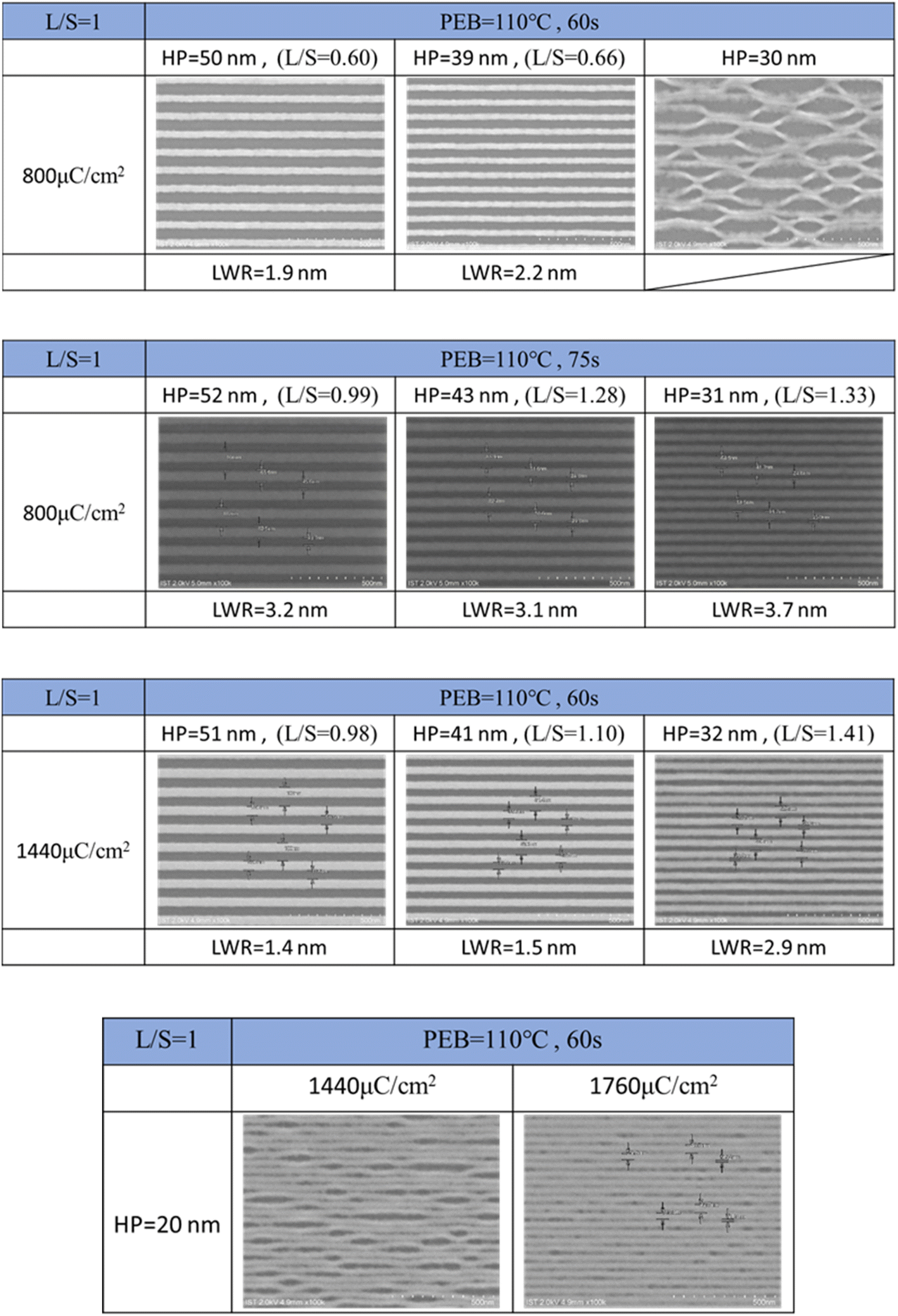
E-beam lithographic patterns were fabricated for cluster (2) under both PAB (80 μC cm−2, 60 s) and PEB conditions (110 °C, 60 s); their SEM images are provided in Fig. 6. Our new cluster (2) was exposed to e-beam doses ranging from 450 to 2720 μC cm−2 across various resolutions (HP = 70–20 nm). SEM images of these patterns are provided in the ESI (Fig. s3).† Under a low J = 800 μC cm−2, cluster (2) can generate a well-defined lithographic pattern with HP = 50 and 39 nm patterns respectively, but a small HP = 30 nm pattern was stripped using an acetone developer to form curved ribbons (see the first row). This delamination pattern can be restored to form a well-defined pattern with an additional 15 s in a new PEB process (the second row). Alternatively, an increased e-beam dose of 1440 μC cm−2 nm−1 enables a clean HP = 30 nm pattern (the third row). A further increase to 1760 μC cm−2 can achieve an even smaller HP = 20 nm pattern (the last row). The line/space (L/S) values at J = 1440 nm μC cm−2 were calculated to be 0.98, 1.10, and 1.31 for HP = 52, 42, and 32 nm patterns, respectively. This trend reflects a typical behavior observed in common photoresists. Additional e-beam patterns, featuring various e-beam doses and HP = 20–70 nm patterns, are provided in the ESI (Fig. S3).†
 | ||
| Fig. 6 SEM images of e-beam lithographic patterns for 6-tin oxide cluster (2); initial thickness 27.8 nm; PAB, 90 °C, 60 s; PEB, 110 °C, 60 s, developer: acetone (10 s). | ||
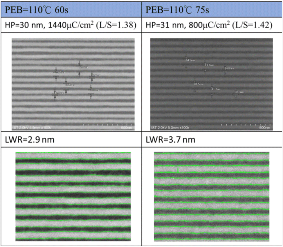
6-Tin oxide cluster (2) is less than the 12-tin oxide cluster (3) in tin density; its superior photosensitivity is unexpected. Line width roughness (LWR) is measured, as this line/edge quality is generally favorable for small metal photoresists. Fig. 7 shows the effects of PEB conditions on e-beam doses and LWR values. With a long PEB duration (110 °C, t = 75 s), an e-beam dose of J = 800 μC cm−2 can produce a mature pattern with HP = 31 nm; the LWR is calculated to be 3.7 nm, showing a good ratio (LWR/HP = 12%). Under mild PEB conditions (110 °C, t = 60 s), a high e-beam dose J = 1440 μC cm−2 is required to form a HP = 30 nm pattern, but the LWR decreased to an outstanding ratio, LWR = 2.9 nm. Accordingly, harsh PEB conditions can reduce the e-beam energy doses, but also deteriorate the line edge quality.
 | ||
| Fig. 7 Line width roughness under different PEB treatments and doses. | ||
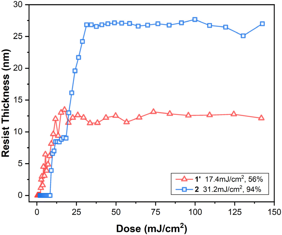
The high photosensitivity toward EUV light is reflected in the contrast curve under different doses; the light exposure was performed with the commercial slots of the Swiss Paul Scherrer Institute Center (PSI) with EUV light at 13.5 nm. The contrast curve in Fig. 8 was measured using acetone as the developer (10 s) without PEB treatment, which well matches a negative-tone photoresist. Cluster 2 takes small EUV doses to develop the EUV pattern; the curve slope is very sharp with the height increasing rapidly to reach the maximum, indicative of high photosensitivity. The threshold energy was 31.2 mJ cm−2 for the cluster (2) to reach the maximum; the height remained at around 27.0 nm from 31.0 to 100 mJ cm−2, corresponding to a small loss (ca. 6%) of height, relative to the initial height (28.8 nm). For the 12-tin oxide cluster (3), the threshold energy was relatively high up to 50 mJ cm−2 without PEB treatment and further decreased to 38 mJ cm−2 under PEB conditions (100 °C, 60 s).13 To our pleasure, this 6-tin oxide cluster (2) appears to be more photosensitive than the 12-tin oxide cluster (3) in both EUV and e-beam lithographic studies. Although the 6-tin oxide cluster (2) has a smaller tin density, a vast number of the embedded Sn2–OH groups accelerate a dehydration process, quickly reducing the solubility. We compared the EUV photolytic behavior of cluster (1′),9 which was previously reported to have a low threshold energy of J = 17.4 mJ cm−2. However, cluster (1′) suffers from significant thickness loss, retaining only 56% (12 nm) of the initial film thickness. We attribute this low EUV dose requirement to rapid radical propagation on the vinyltin moieties. Despite EUV lithography, the film of cluster (1′)9 retains nearly the same amount of carboxylate ligands, resulting in only minor solubility changes in the acetone developer. In contrast, the EUV-promoted aggregation of cluster (2) primarily relies on a dehydration reaction, as revealed by our mechanistic study (vide infra). The loss of two Sn–OH groups to form a Sn–O–Sn unit significantly reduces the resist solubility in the acetone developer, enhancing thickness retention.
 | ||
| Fig. 8 Contract curves of clusters (1′) and (2) under different EUV doses. The initial thickness is 24.2 and 29.1 nm for clusters (1′) and (2) respectively. | ||
Development of EUV lithographic patterns was performed with PEB treatment (110 °C. 90 s); the developer is acetone with a 10 s rinse. The EUV exposure was performed with an interference mask containing dense line/space patterns of 16–50 nm half-pitches. Fig. 9 depicts several SEM images, in which the resolutions are resolved into HP = 35, 25, 19, and 16 nm respectively. Additional SEM images on different EUV doses (40–90 mJ cm−2 and HP = 16–52 nm) are provided in the ESI (Fig. S4).† The threshold energy in the EUV contrast curve in Fig. 6 is relatively small ca. 31.5 mJ cm−2; the SEM images of selected EUV patterns in Fig. 7 show no sign of top loss for the lithographic patterns including HP = 35 and 25 nm; the exposed photoresist is well mature to resist the etching toward the acetone developer. A notable feature is the line/space parameters (L/S), which are 1.06, 1.18, 0.98, and 0.89 for the HP = 35 nm, 25 nm, 19 nm, and 16 nm patterns. These L/S values are close to the idealized value L/S = 1. Small L/S values (0.98–0.89) at HP = 19 and 16 nm indicate that additional EUV doses can produce more qualified patterns with increased thickness.
 | ||
| Fig. 9 SEM images of the EUV lithographic patterns for 6 = tin oxide cluster (2); initial thickness 27.2 nm; PAB, 90 °C 60 s, PEB (110 °C, 90 s), developer: acetone (10 s). | ||
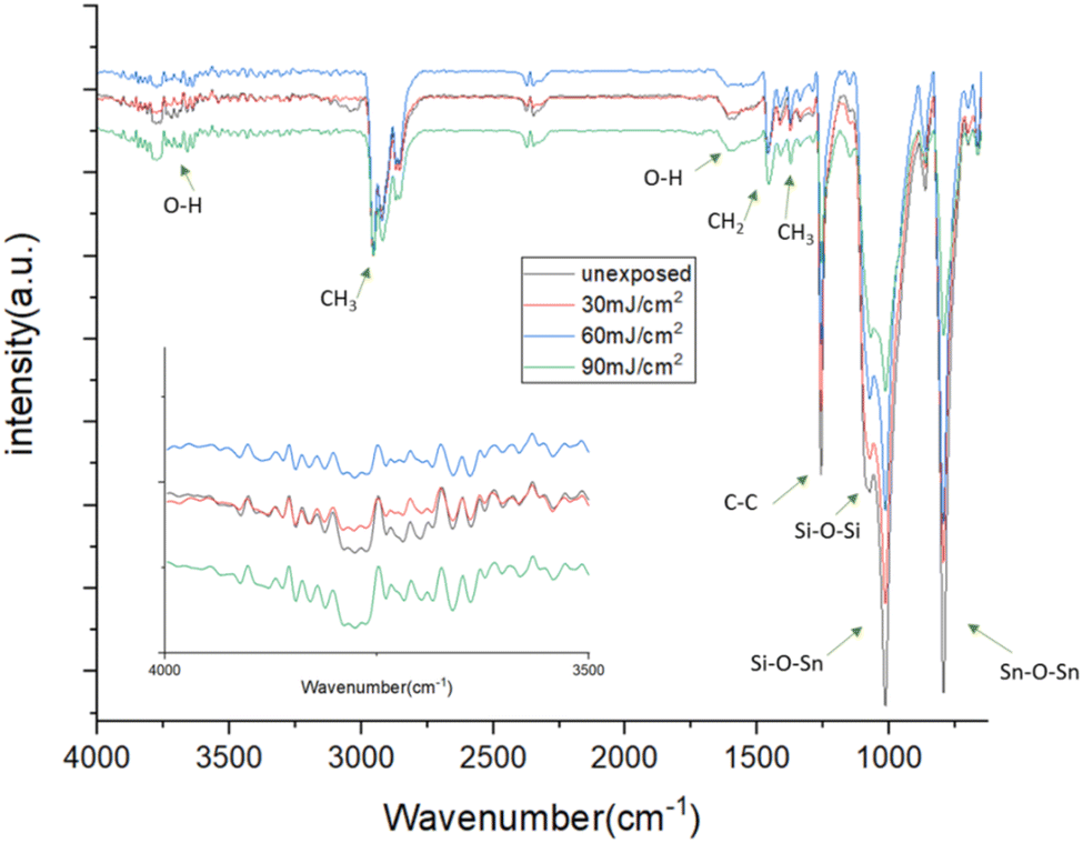
FTIR in ATR (attenuated total reflectance) mode was used as a tool to study the mechanism under EUV light. A film was prepared in 1.5 μm in thickness before the PAB process (90 °C, 60 s). The IR signal sensitivity is generally lower compared to that of XPS studies. After moderate or high EUV doses, the remaining organic species are present in small concentrations, necessitating a thick film. After EUV exposures at 0, 30, 60, and 90 mJ cm−2, the spot of the EUV exposure could not be identified unless the films were developed with acetone for 8 s. In contrast with the Sn–OH band at 3600–3850 nm, the band in the 3200–3400 cm−1 region is very weak; the latter is associated with a hydrogen bonded Sn–OH group. As shown in Fig. 10, the IR absorption bands at J = 30–90 mJ cm−2 were depicted with the ν(C–H) band of equal intensities, in order to manifest the effect of EUV doses on the Sn–O bands in the 1100–1000 and 500–600 cm−1 regions. Absorption bands at 1000–1100 cm−1 are due to the Si–O–Sn or Si–OH–Sn absorption; this information suggests that the exposed spot is stripped by the acetone developer. As the EUV doses are increased, the two bands of the Si–O–Sn and Sn–O–Sn absorption intensities decrease gradually. The same trend is also noted for the Sn–OH bands in the 3500–4000 cm−1, showing decreasing intensity. These spectral changes reveal the following information: (i) the Sn–O band loss is more significant than the Sn–butyl loss and (ii) EUV light can enhance the dehydration of the Sn–OH, Si–OH–Sn, and Sn–OH–Sn moieties.
 | ||
| Fig. 10 FTIR spectra of cluster (2) at different EUV doses. | ||
HRXPS (high resolution X-ray photoelectron spectroscopy) was used as a probe to study the effect of EUV doses on the element compositions of the film surface. The films were treated with a PAB process before the EUV exposure (90 °C, 60 s). Herein, we assume that the formula of cluster (2) is nearly the same as that of the pristine sample although a small degree of dehydration occurred in the PAB process (see Fig. 3). We observed no Si-binding energy because a small thickness (30 nm) warrants a smooth surface. After exposure to different EUV doses, these samples were opened to air before being stored in a nitrogen-filled container. Fig. 11 shows the HRXPS spectra of the thin films at J = 0–120 mJ cm−2. At a J = 30 mJ cm−2 dose, a loss of six carbon and three oxygen atoms occurred; with J = 60–120 mJ cm−2, the loss of carbon atoms becomes slow whereas the oxygen atoms remain constant if standard error is considered. The changes in element composition are well rationalized by two EUV-promoted reactions, including (i) oxidative cleavage of Sn–butyl bonds and (ii) dehydration of Sn–OH or Sn2OH bonds. A typical EUV induced Sn–butyl cleavage followed by air treatment will lead to a loss of carbon atoms accompanied by increased oxygen atoms.
 | ||
| Fig. 11 Composition analysis using HRXPS at different EUV doses. | ||
The photolytic mechanism of cluster (2) is elucidated by HRXPS analysis of the O(1s) component. There are two separate peaks at 530.5 eV and 529.0 eV, assignable to the Sn2–OH and Sn2O according to the literature data of [(BuSn)12O14(OH)6](OH)2 (3).31–33 Notably, the distribution of oxygen contents varies with increasing EUV doses. As shown in Fig. 12, the SnOH groups including Sn–OH and Sn2OH gradually decreased in content from 54% to 43.6% with increasing EUV doses from J = 30 to 120 mJ cm−2 whereas the dehydrated forms such as Sn2O or Sn3O increased in content from 46% to 56.4%. This observation supports the role of EUV-inspired dehydration, which is also inferred by FTIR and composition studies by XPS studies in Fig. 11.
 | ||
| Fig. 12 Band shape fitting of the O(1s) component of cluster (2) at different EUV doses. | ||
We prepared two photoresists, clusters (1′) and (2), representing carboxylate-containing and carboxylate-free tin clusters, respectively, to evaluate their etch resistance using reactive ion etching (RIE) methods. Both materials were coated onto a 100 nm-thick SiO2 layer over silicon wafers. After a post-applied bake (PAB) process, the initial thicknesses were measured to be 30.8 nm for cluster (2) and 25.9 nm for cluster (1′) (Fig. 13). The films were exposed to an e-beam dose of 600 μC cm−2 for cluster (2) and 250 μC cm−2 for cluster (1′). Following exposure, the films were developed using heptanone for cluster (1′) (60 s) and acetone for cluster (2) (10 s) to create a 200 × 200 μm2 square pattern for subsequent etching tests.
 | ||
| Fig. 13 Comparison of etching resistance between clusters (1′) and (2). | ||
A hard bake was performed at 200 °C for 60 seconds, reducing the thickness to 19.6 nm for cluster (2) and 17.2 nm for cluster (1′). The films were then exposed to a CHF3/O2 gas mixture for 15 seconds, and the height loss was used to determine their etching rates. Specific data are shown in Fig. 13. The etching rate of cluster (2) was found to be 2.1 times slower than that of cluster (1′). The selectivity, S = RateSiO2/RatePR, for cluster (2) was calculated to be S = 1.53, which is significantly higher than the S = 0.73 value observed for cluster (1′).
Cluster (2) has a moderate size but its photosensitivity is better than the 12-Sn oxide cluster (3); a vast number of hydroxyl groups on the cluster is likely to be the key factor due to the ease of thermal and photo-inspired dehydration reactions. Out FTIR studies in Fig. 10 reveal that the loss of the n-butyl group is less in amount than that of oxygen atoms, indicating a key process involved a dehydration reaction. This assessment is again supported by the O(1s) component analysis in Fig. 12, in which the Sn–OH contents decrease more significantly with increasing EUV doses. Particularly notable is the loss of carbon and oxygen contents as shown in Fig. 11. A typical photolytic cleavage of Sn–butyl bonds will lead to a significant decrease in carbon contents whereas the oxygen contents are often increased because of a re-oxidation of Sn(III) species by H2O/O2 after exposure to O2/H2O. Our experimental data in Fig. 10–12 strongly support EUV-inspired dehydrations of several different Sn–OH groups as depicted in Scheme 2. Such dehydration reactions are confirmed to be faster than the Sn–butyl cleavage.
 | ||
| Scheme 2 Proposed chemical reactions with EUV exposure. | ||
Surface reactions between the interfaces are informative according to our FTIR studies. Cluster (2) in KBr pellets shows a strong and broad absorption at 3403 and a shadow at 3651 cm−1, as depicted in Fig. 2, indicating that most of Sn–OH groups are hydrogen bonded. With coating on a SiO2 wafer, the broad peak of cluster (2) at 3403 cm−1 becomes very weak whereas the peak at 3646 cm−1 becomes strong and sharp. Meanwhile, we observe a new (Sn–O–Si) band at 1074 cm−1 (see Fig. 3). Accordingly, we postulate that there is an interface reaction between the Si–OH and Sn–OH groups to form Si–O–Sn species. Furthermore, Si(IV) is more electron negative than Sn(IV); the Si–O oxygen is expected to be less basic, thus enabling the formation of hydrogen-bonded Sn–OH groups.
Conclusions
EUV-fabrication of lithographic SnO2-nanostructures1–6,28 is the current trend as traditional SiO2 lithography costs very high EUV energies. Before this work, [(BuSn)12O14(OH)6](OH)2 (3) was the only reported carboxylate-free cluster and is a widely used photoresist to fabricate high-resolution SnO2-like patterns toward the e-beam and EUV light. This work reports a new 6-tin oxide cluster (BuSn)6O4(OH)10,(2) which is better than the 12-oxide cluster (3) not only in the film roughness but also in the photosensitivity of e-beam and EUV exposure. In the e-beam lithographic pattern, cluster (2) can be fabricated with a small HP = 21 nm pattern at J = 1760 μC cm−2. Its EUV lithography has been obtained with a high-resolution pattern (HP = 16 nm) at J = 56 mJ cm−2. Mechanistic studies by both FTIR and HRXPS over various EUV doses reveal that molecular aggregation of photoresist 2 proceeds predominantly on the dehydration of two Sn–OH moieties whereas the Sn–butyl cleavage is not significant. FTIR also unveils a surface reaction between Si–OH and Sn–OH, giving new Sn–O–Si absorption peaks.We also evaluated the photoresist performance of cluster (2) compared to a carboxylate-containing cluster (1′),9 both of which are efficient EUV photoresists. Cluster (1′) and its family member (1) exhibit low SnO2 content and the presence of volatile Sn species, reflecting their material limitations. Following EUV lithography, the mature film thickness of the carboxylate-free cluster (2) is nearly double that of cluster (1′). In etching resistance tests, cluster (2) significantly outperforms cluster (1′) in SiO2-contrast selectivity, with a respective selectivity ratio of S = 1.53:0.73. These results indicate that the synthesis of carboxylate-free photoresists, such as clusters (2) and (3), represents a promising direction for future commercial applications.
Experimental section
Material preparation and characterization
All chemicals were purchased from the Sigma company without further purification. FTIR spectra in the KBr pellet were obtained with a Vertex 80v spectrometer (Bruker). 119Sn 1H and 13C NMR spectra were recorded on a Bruker 500 or 400 MHz spectrometer with CDCl3 as the internal standard. The chemical shifts of 119Sn NMR spectra are referred to Me4Sn (0.0 ppm). A Mettler-Toledo 2-HT was used to measure TGA at a heating rate of 8 °C min−1.Thin-film deposition
A 4-methylpentan-2-ol solution of cluster 2 at 1.5 wt% was filtered through a 0.22 μm PTFE syringe filter. The solution was deposited on a silicon wafer coated with a SiO2 layer (THK = 100 nm), followed by spin-coating at 1200 rpm for 10 s and 1600 rpm for 25 s. The wafer was baked at 90 °C for 60 s for all samples. The thickness of these films is around 27–28 nm, which were measured using a J. A. Woollam M2000. Atomic force microscopy (AFM) images were obtained with a SEIKO SPA-300 HV, using the contact mode.Electron-beam lithography (EBL)
An electron-beam energy source was generated on an Elionix ELS-7800 with an accelerating voltage of 80 kV and a beam current of 200 pA for the contrast curve and 50 pA for the line pattern. After e-beam exposure, the samples were developed with acetone or 2-heptanone for 20 or 60 s before rinsing with deionized water. The contrast curve of the photoresist was obtained on a series of squares (50 × 50 mm2), each with e-beam dosages at 80 to 2400 μC cm−2. After solvent development, the remaining thickness of each exposed area was measured through an α-step tool, providing the data of the contrast curve. The resolution limit of e-beam lithography is designed from 50 nm HP down to 20 nm HP.EUV-IL lithographic studies
An EUV interference lithography (EUV-IL) system involving two-beam interference is used to produce periodic aerial images. The EUV-IL exposure was performed at the Swiss Light Sources (SLS), Paul Scherrer Institute, with 13.5 nm light with a high spatial coherence length and uniform illumination, to transmit a grating mask. This mask comprises multiple grating pairs ranging from 100 nm HP to 32 nm HP. The period of the first-order interference on the resist is half of that on the mask grating. The dosage on the mask (Dosemask) ranges from 20 mJ cm−2 to 150 mJ cm−2 with 5 mJ cm−2 increments. The dosage on the resist (Doseresist) needs to be divided into Dosemask with tool factors corresponding to various grating pairs. ATR-FTIR and HRXPS studies were performed at the National Synchrotron Radiation Research Center, Taiwan (NSRRC); the exposure of photoresist films to EUV light is without any mask on the TLS 21B2 line.Pattern development
After EUV or e-beam exposure, the films were baked at 110 °C for 60 s before cooling at room temperature. The pattern was developed with 2-heptanone or acetone before baking at 110 °C for 90 s.Measurement of edge etching rates
A home-made RIE system (CNT-RPA08 from Creating Nano Technologies Inc.) was used to test the etching rate of the studied photoresist and SiO2. The etching recipe is 50 sccm CHF3 with 10 sccm O2 under 200 mTorr at a power of 150 W for 15 s. The samples of photoresists (1′) and (2) are prepared using the e-beam and mounted on the SiO2 layer, as described in the text. All thickness data were measured using alpha-step (DektakXT, Bruker) and ellipsometer (M2000, J. A. Woollam) techniques.FT-IR measurement
Photoresist 2 was coated on a 2.4 × 5 cm2 silicon wafer by spreading a 4-methylpentan-2-ol solution (3.5 wt%, 0.9 mL) over this wafer substrate. The thickness is measured to be 1.5 μm. This film was dried in air at room temperature for 36 h. Another coated film was baked at 90 °C for 60 s. After EUV exposure, the two films were developed with acetone for 5 s to show the exposed area before baking at 90 °C for 90 s. The operation of FTIR was performed in the air on a Bruker model Tensor 27 containing a KBr beam splitter. The IR signals were then collected with an MCT (mercury cadmium telluride) detector in transmission mode; the resolution is 4 cm−1.High-resolution X-ray photoelectron spectroscopy (HRXPS)
HRXPS data were obtained on a ULVAC-PHI Quantera II, with a monochromatic Al Kα source (energy of 1486.6 eV). A survey spectrum was obtained with a pass energy of 280 eV and an energy step of 1 eV; a pass energy of 55 eV and an energy step of 0.1 eV were used for O, C, and Sn high-resolution spectra. The films were prepared by the same procedure as described in e-beam and EUV studies. The films were baked at 90 °C for 60 s for EUV exposure at the NSRRC center, Taiwan. After exposure, standard development was performed with acetone for 20 s before baking at 90 °C for 90 s. This film is used for HRXPS study.Procedure for synthesis of cluster (1)
To a DCM (20 mL) solution of butyltrichlorostannane (0.50 g, 1.80 mmol) acetic silver salt (0.90 g, 5.4 mmol) was added. The mixture was then stirred at 40 °C for 8 h. For this reaction mixture was cooled to room temperature before filtration. The filtrate was concentrated under reduced pressure. Recrystallization of this crude product using hexane/DCM afforded cluster (1) as a colorless solid (65%).Procedure for synthesis of cluster (2)
Cluster 1 (300 mg, 0.18 mmol) in THF (20 mL) was treated with LiOH (0.5 M, 5 mL) at 0 °C and the mixture was stirred for 20 min. The solution was concentrated under reduced pressure to a reduced volume of ca. 5 mL The solution was extracted with a mixing solvent of DCM/H2O (1:1, 10 mL) three times; the combined DCM layer was dried in vacuo before addition of hexane to yield cluster 2 as a white precipitate (53 mg, 0.041 mmol, 23% yield). Elemental analysis, 1H, 13C, and 119Sn NMR and TGA spectra and their spectral data are provided in the ESI.†
Data availability
All data associated with this work can be found in the Experimental section of this manuscript.Author contributions
J.-H. Liu is responsible for the design of all synthetic work. T.-S. Gau and B.-J. Lin are in charge of the lithographic development. P.-W. Chiu and B.-H. Chen conducted e-beam lithographic work. C.-F. Chou, C.-D. Li, and Y.-F. Tseng were responsible for the synthesis and spectroscopic studies of photoresists. S.-Z. Chen, S.-L. Tsai and W.-B. Jian performed edge etching experiments using an e-beam source and the RIE method. The chief investigator, Jui-Hsiung Liu, is the passport name of Rai-Shung Liu; the patent laws of Taiwan and the USA must use passport names for patent applications.Conflicts of interest
There are no conflicts to declare.Acknowledgements
The authors thank the National Science and Technology Council (NSTC), Taiwan, and Taiwan Semiconductor Manufacturing Company (TSMC) for financial support of this project. The availability of commercial slots at the Swiss Light Sources (SLS), Paul Scherrer Institute, is also acknowledged. We also thank NSRRC, Taiwan, for the EUV-beam service.References
- J. Stowers and D. A. Keszler, Microelectron. Eng., 2009, 86, 730–733 CrossRef CAS.
- N. Mojarad, J. Gobrecht and Y. Ekinci, Sci. Rep., 2015, 5, 9235 CrossRef CAS PubMed.
- L. Li, X. Liu, S. Pal, S. Wang, C. K. Ober and E. P. Giannelis, Chem. Soc. Rev., 2017, 46, 4855–4866 RSC.
- H. Xu, K. Sakai, K. Kasahara, V. Kosma, V. K. Yang, H. C. Herbol, J. Odent, P. Clancy, E. P. Giannelis and C. K. Ober, Chem. Mater., 2018, 30(12), 4124–4133 CrossRef CAS.
- G. Lim, K. Lee, S. Choi and H. J. Yoon, Coord. Chem. Rev., 2023, 493, 215307 CrossRef CAS.
- A. Develioglu, M. Vockenhuber, L. Van Lent-Protasova, I. Mochi, Y. Ekinci and D. Kazazis, Proc. SPIE, 2023, 12750, 1275008 Search PubMed.
- P.-C. Liao, P.-H. Chen, Y.-F. Tseng, T.-A. Shih, T.-A. Lin, T.-S. Gau, B.-J. Lin, P.-W. Chiu and J.-H. Liu, J. Mater. Chem. C, 2022, 10, 15647–15655 RSC.
- Y.-F. Tseng, P.-C. Liao, P.-H. Chen, T.-S. Gau, B.-J. Lin, P.-W. Chiu and J.-H. Liu, Nanoscale Adv., 2024, 6, 197–208 RSC.
- J.-R. Wu, T.-A. Lin, Y.-R. Wu, P.-H. Chen, T.-S. Gau, B.-J. Lin, P.-W. Chiu and R.-S. Liu, Nanoscale Adv., 2023, 5, 3033–3043 RSC.
- C.-D. Li, T.-A. Lin, P.-H. Chen, T.-S. Gau, B.-J. Lin, P.-W. Chiu and J.-H. Liu, Nanoscale Adv., 2024, 6, 2928–2944 RSC.
- H. Xu, K. Sakai, K. Kasahara, V. Kosma, K. Yang, H. C. Herbol, J. Odent, P. Clancy, E. P. Giannelis and C. K. Ober, Chem. Mater., 2018, 30, 4124–4133 CrossRef CAS.
- N. Thakur, M. Vockenhuber, Y. Ekinci, B. Watts, A. Giglia, N. Mahne, S. Nannarone, S. Castellanos and A. M. Brouwer, ACS Mater. Au, 2022, 2, 343–355 CrossRef CAS PubMed.
- B. Clark, M. Kocsis, M. Greer, A. Grenville, T. Saito, L. Huli, R. Farrell, D. Hetzer, S. Hu, H. Matsumoto, A. Metz, S. Kawakami, K. Matsunaga, M. Enomoto, J. Lauerhaas, A. Ratkovich and D. DeKraker, Proc. SPIE, 2015, 9425, 94251A–1 CrossRef.
- Y. Ekinci, H. H. Solak, C. Padeste, J. Gobrecht, M. P. Stoykovich and P. Nealy, Microelectron. Eng., 2007, 84, 700–704 CrossRef CAS.
- A. Rathore, I. Pollentier, M. Cipriani, H. Singh, D. D. Simone, O. Ingolfsson and S. De Gendt, ACS Appl. Polym. Mater., 2021, 3, 1964–1972 CrossRef CAS.
- B. Cardineau, R. D. Re, M. Marnell, H. Al-Mashat, M. Vockenhuber, Y. Ekinci, C. Sarma, D. A. Freedman and R. L. Brainard, Microelectron. Eng., 2014, 127, 44–50 CrossRef CAS.
- B. Cardineau, R. D. Re, M. Marnell, H. Al-Mashat, M. Vockenhuber, Y. Ekinci, C. Sarma, D. A. Freedman and R. L. Brainard, Proc. SPIE, 2014, 9051, 90511B CrossRef.
- A. M. Brouwer, J. Photopolym. Sci. Technol., 2022, 35, 81–86 CrossRef CAS.
- J. H. Ma, C. Needham, H. Wang, A. Neureuther, D. Prendergast and P. Naulleau, ACS Appl. Mater. Interfaces, 2022, 14, 5514–5524 CrossRef CAS PubMed.
- J. Haitjema, M. Zhang, M. Vockenhuber, D. Kazazis and Y. Ekinci, J. Micro/Nanolithogr., MEMS, MOEMS, 2017, 16, 033510–033517 Search PubMed.
- I. Bespalov, Y. Zhang, J. Haitjema, R. M. Tromp, S. J. van der Molen, A. M. Brouwer, J. Jobst and S. Castellanos, ACS Appl. Mater. Interfaces, 2020, 12, 9881–9889 CrossRef CAS PubMed.
- N. Kenane and D. A. Keszler, ACS Appl. Mater. Interfaces, 2021, 13(16), 18974–18983 CrossRef CAS PubMed.
- M. C. Sharps, R. T. Frederick, M. L. Javitz, G. S. Herman, D. W. Johnson and J. E. Hutchison, Chem. Mater., 2019, 31, 4840–4850 CrossRef CAS.
- N. Kenane, M. A. Grove, C. K. Perkins, T. R. Reynolds, P. H. Cheong and D. A. Keszler, Inorg. Chem., 2020, 59, 3934–3941 CrossRef CAS PubMed.
- J. T. Diulus, R. T. Frederick, D. C. Hutchison, I. Lyubinetsky, R. Addou, M. Nyman and G. S. Herman, ACS Appl. Nano Mater., 2020, 3, 2266–2277 CrossRef CAS.
- R. T. Frederick, S. Sahab, J. T. Diulus, F. Luo, J. M. Amador, M. Li, D. -H Park, E. L. Garfunkel, D. A. Keszler and G. S. Herman, Microelectron. Eng., 2019, 205, 26–31 CrossRef CAS.
- A. D. O. Jorgetto, M. V. Boldrin and M. O. Orlandi, Sci. Rep., 2023, 13, 14774 CrossRef CAS PubMed.
- J. Haitjema, L. Wu, A. Giuliani, L. Nahon, S. Castellanos and A. M. Brouwer, Phys. Chem. Chem. Phys., 2021, 23, 20909 RSC.
- P. Piszczek, A. Radtke, A. Grodzicki, A. Wojtczak and J. Chojnacki, Polyhedron, 2007, 26, 679–685 CrossRef CAS.
- D. De Simone, M. Mao, M. Kocsis, P. De Schepper, F. Lazzarino, G. Vandenberghe, J. Stowers, S. Meyers, B. L. Clark, A. Grenville, V. Luong, F. Yamashita and D. Parnell, Proc. SPIE, 2016, 9776, 97660B Search PubMed.
- Y. Zhang, J. Haitjerna, X. Liu, F. Johansson, A. Lindblad, S. Castellanos, N. Ottosson and A. M. Brouwer, J. Micro/Nanolithogr., MEMS, MOEMS, 2017, 16(2), 023510 CrossRef.
- G. Lim, K. Lee, C. Koh, T. Nishi and H. J. Yoon, ACS Mater. Au, 2024, 4, 468–478 CrossRef CAS PubMed.
- Y. Zhang, J. Haitjema, X. Liu, F. Johansson, A. Lindblad, S. Castellanos, N. Ottosson and A. M. Brouwer, J. Micro/Nanolithogr., MEMS, MOEMS, 2017, 16, 023510 CrossRef.
Footnote |
| † Electronic supplementary information (ESI) available. See DOI: https://doi.org/10.1039/d4na00651h |
| This journal is © The Royal Society of Chemistry 2025 |