
Multifunctional polymers with biomimetic compound architectures via nanoporous AAO films for efficient solar energy harvesting in dye-sensitized solar cells†
Bhaskar Dudem‡
,
Jung Woo Leem‡,
Joo Ho Lim,
Soo Hyun Lee and
Jae Su Yu*
Department of Electronics and Radio Engineering, Kyung Hee University, 1732 Deogyeong-daero, Giheung-gu, Yongin-si 446-701, South Korea. E-mail: jsyu@khu.ac.kr
First published on 6th October 2015
Abstract
We report the considerable enhancement of the solar power conversion efficiency (PCE) in dye-sensitized solar cells (DSSCs) using polydimethylsiloxane (PDMS) patterned with a novel biomimetic compound architecture (CA) (i.e., hierarchical nanobumps/microcone arrays) with light-harvesting and self-cleaning functions as a protective cover-layer. The CA-PDMS is transferred from a nanoporous anodic alumina oxide mold by a facile and cost-effective soft imprint lithography via a microcone-patterned sapphire substrate. A lamination of CA-PDMS on the glass leads to increased total and diffuse transmittance properties (i.e., antireflection and light scattering effects), simultaneously, compared to bare glass over a wide wavelength range of 350–800 nm, exhibiting a much larger solar weighted total transmittance (TSW) value of ∼94% and an average haze ratio (HA) value of ∼49.7% (TSW ≈ 90.4% and HA ≈ 1.4% for bare glass). In addition, sand grains on the hydrophobic surface with a water contact angle of ∼134° are clearly washed by rolling down water droplets (i.e., self-cleaning effect). To simply demonstrate the device applicability, CA-PDMS is introduced onto an outer surface of the front glass substrate in a DSSC. The resulting DSSC with CA-PDMS exhibits a boosted PCE value of ∼8.24% mainly due to a strongly increased short-circuit current density (JSC) value of ∼18.11 mA cm−2 compared to the reference DSSC with bare glass (PCE ≈ 7.45% and JSC ≈ 16.37 mA cm−2) under AM1.5G illumination, indicating a large PCE enhancement percentage value of ∼10.7%.
Introduction
Techniques to harvest energy from renewable energy sources including sunlight, wind, biomass, geothrmal heat, tide, etc. have been increasingly crucial to overcome the energy crisis, environmental pollution, and global warming throughout the world due to their more extensive exploitation possibilities compared to the conventional power supply using fossil fuels.1–3 Particularly, among these, solar energy has been considered as an outstanding renewable power source because of its safety, cleanliness (e.g., pollution-, waste-, and noise-free), and unlimited supply.4,5 Its application fields are also very extensive from small power fields such as portable and mobile electronic equipment to large electrical power generating plants. Over the past few years, tremendous efforts have been made to boost the power conversion efficiency (PCE) of dye-sensitized solar cells (DSSCs) due to their technical feasibility and cost-effectiveness as alternatives to silicon or III–V material-based solar cells.6,7 In order to improve the spectral sensitivity and the PCE of DSSCs, many studies have reported on various approaches: optimizing sensitizers,8 using nanostructured active layers themselves as scattering layers,9 using photonic crystals,10 optimizing the active layer thickness,11 and increasing the concentration of the attached dye molecules.12 Additionally, an undyed layer placed on the top of the active layer13 or a mirror-like platinum (Pt) counter electrode as an internal rear reflector14 was also studied. Among various strategies for increasing solar energy harvesting in DSSCs, one simple method is to enhance the light absorption in the active layer of the devices over a wide spectral range of sunlight by introducing an antireflective (AR) and light-scattering layer on the externally facing surfaces of the transparent substrates such as glasses and plastics.15–19 Recently, for this, biomimetic architectures consisting of nano, micro, or compound (e.g., hierarchical nano/micro configurations) structures have been widely studied in several solar cells.20–24 In particular, compound structures strongly enhance the optical behaviors (e.g., antireflection, transmission, and diffuse light scattering) of the transparent substrates over a wide range of wavelengths and incident angles.25–29 With a compound architecture (CA), the microstructure extends the optical path of the light and promotes a diffuse light-scattering transmission resulting from higher orders of diffracted waves, while maintaining a high total (i.e., specular and diffuse) transmission.30 On the other hand, nanostructures with a period smaller than the wavelength of the incident light allow for only the zeroth order of the diffracted wave and act as a homogeneous medium with a gradient-refractive-index (GRIN) profile between the air and the material, thus further effectively suppressing the Fresnel reflection at the surface.31,32 Therefore, the introduction of compound structures into the solar cells would lead to the increase of the overall light absorption in the active layer, and thus the solar power generation of DSSCs could be enhanced. However, for the realization of these multi-scale compound structures, complicated and expensive fabrication methods including patterning and etching processes are mostly required, which causes an increase in the fabrication cost and time, including a scale limitation.25–29 A cost-effective, simple, and fast soft imprint lithographic (SIL) patterning method makes it possible to relatively easily form artificial compound structures on the surface of transparent substrates using ultraviolet or thermal curable polymers.33–36 Although the master molds are also prepared by lithography patterning and etching processes, once the molds and the replica polymer stamps are made, they can be repeatedly used for pattern transfers into secondary substrates. Furthermore, large-scale fabrication techniques (i.e., roll-to-roll and roll-to-plate processes) of the master molds and stamps have been developed in SIL,37 which would facilitate mass-production for industry applications. In general, polydimethylsiloxane (PDMS) has often been used to transfer multi-scale patterns precisely on other substrates due to its low free surface energy, flexibility, transparency, and hardness.33–39 For transparent substrates, CA-PDMS can be used since it is not only easily laminated on a planar surface, but also simply detached from it. Furthermore, as a protective cover-layer, it can improve the optical properties of transparent substrates because of its lower refractive index (n ≈ 1.43),40 which could enhance the photo-generated currents in DSSCs. To form a desirable CA-PDMS, a mold with the negative of the compound structure, which is usually prepared by nano- and micro-lithography patterning and etching, is required. Actually, the formation of nanostructures rather than microstructures on the surface of the molds gives rise to an increase in fabrication complexity and cost because they are generally fabricated by expensive electron (e)-beam, nanoimprint, and laser interference lithography or post-heat/chemically treated colloidal spheres and metal nanoparticles with a subsequent dry etching process (e.g., reactive ion etching or inductively coupled plasma etching system). But, if electrochemical oxidation of aluminum (Al) films is employed in a particular acidic electrolyte solution, nanostructures on the microstructured molds can be easily and cost-effectively fabricated without any dry etching processes.41,42 Meanwhile, self-cleaning properties have been found to be useful in removing any surface pollutants for high-performance devices in practical external applications.20,33 Thus, the surface wetting behavior of CA-PDMS is also important. Several studies have reported the efficient antireflection characteristics of nano, micro, or compound structured polymer films, which were prepared using the SIL method,34,43,44 as well as the PCE improvement of organic and inorganic solar cells by utilizing them on the surface of transparent substrates as a protective cover-layer.20,33,45,46 However, there are very few or no reports on the use of CA consisting of hierarchical nanostructures on microstructured arrays on the surface of polymer films as multifunctional (i.e., light-harvesting and self-cleaning) protective cover-layers of glass substrates in DSSCs using porous anodic alumina oxide (AAO) templates with a negative CA as a master mold via the SIL method. So, it is very meaningful to study the photovoltaic performance of the DSSCs containing compound structured polymer films on the outer glass surface, including their optical and surface wetting properties. In this work, we fabricated artificial biomimetic compound structures consisting of hierarchical nanobumps on microcone arrays on the surface of PDMS using the SIL method via AAO molds imprinted from patterned sapphire substrate (PSS) with microcone arrays. The fabricated CA-PDMS was laminated on the glass substrates and its optical and self-cleaning behaviors were characterized. For a theoretical analysis of the optical light scattering properties, finite-difference time-domain (FDTD) simulations were also performed. Finally, to simply show the practical feasibility in solar cell devices, the fabricated CA-PDMS was applied to the glass substrates of DSSCs as a protective cover-layer and their device current–voltage (J–V) curves and incident photon to current conversion efficiency (IPCE) spectra were explored.Experimental and numerical modelling details
Fabrication of AAO molds
0.25 mm-thick Al sheets (99.999% purity, Alfa Aesar) with a size of 3 × 3 cm2 were cleaned using ultra-sonication with acetone, ethanol and de-ionized (DI) water for 10 min, and subsequently dried under a stream of argon. To reduce the surface roughness, the Al sheets were electro-polished in a mixture of perchloric acid and ethanol (HClO4![[thin space (1/6-em)]](https://www.rsc.org/images/entities/char_2009.gif) :C2H5OH = 1:4 in volume ratio) with a voltage of 15 V, which was applied between the anode (Al) and cathode (Pt) for 5 min, at an electrolyte temperature of 5 °C. Two-dimensional (2D) periodic inverted microcone arrays on the surface of the Al sheets (i.e., IMc-Al mold) were formed using a commercial microcone-PSS (Mc-PSS), which was fabricated using a conventional photolithography and subsequently an inductively coupled plasma dry etching process with BCl3/He mixture gases, purchased from AND Co. using an imprinting method with an applied pressure of 25 MPa at a temperature of 210 °C. After that, the IMc-Al molds were anodized in a 3 wt% phosphoric acid (H3PO4) solution at 0 °C for 25 min under an applied voltage of 120 V. To widen the pore diameter, the anodized samples were additionally dipped into a 5 wt% H3PO4 solution at 30 °C for 8 min, creating AAO molds with hierarchical inverted nanopore/microcone (compound) architectures (i.e., ICA-AAO molds). The AAO molds with nanopores (i.e., Np-AAO molds) with a large pore size were prepared from the electro-polished Al sheets using the same anodization process.
:C2H5OH = 1:4 in volume ratio) with a voltage of 15 V, which was applied between the anode (Al) and cathode (Pt) for 5 min, at an electrolyte temperature of 5 °C. Two-dimensional (2D) periodic inverted microcone arrays on the surface of the Al sheets (i.e., IMc-Al mold) were formed using a commercial microcone-PSS (Mc-PSS), which was fabricated using a conventional photolithography and subsequently an inductively coupled plasma dry etching process with BCl3/He mixture gases, purchased from AND Co. using an imprinting method with an applied pressure of 25 MPa at a temperature of 210 °C. After that, the IMc-Al molds were anodized in a 3 wt% phosphoric acid (H3PO4) solution at 0 °C for 25 min under an applied voltage of 120 V. To widen the pore diameter, the anodized samples were additionally dipped into a 5 wt% H3PO4 solution at 30 °C for 8 min, creating AAO molds with hierarchical inverted nanopore/microcone (compound) architectures (i.e., ICA-AAO molds). The AAO molds with nanopores (i.e., Np-AAO molds) with a large pore size were prepared from the electro-polished Al sheets using the same anodization process.
Fabrication of NbA-, McA- and CA-PDMS
A hard PDMS (h-PDMS) solution, which was prepared by mixing VDT-731 (Gelest, Inc.) and HMS-301 (Gelest, Inc.) copolymers, was spin-casted onto the Np-AAO molds, IMc-Al molds, and ICA-AAO molds, and then cured at 80 °C for 30 min. Afterwards, a Sylgard 184 (Dow Corning Co.) mixed soft PDMS (s-PDMS) solution with a ratio of 10:1 (base:agent) was poured onto the corresponding h-PDMS/molds, and subsequently cured at 80 °C for 3 h. Finally, the PDMS (h-PDMS/s-PDMS) was carefully peeled off the molds, thus producing nanobump architecture- (NbA-), microcone architecture- (McA-), and CA-PDMS.
Preparation of DSSCs
DSSCs with an active area of 0.5 × 0.5 cm2 were conventionally fabricated by drop-casting polymer electrolyte solution onto the photoanode and covering the device with the counter electrode. 15 μm-thick TiO2 particles (PST-18NR, CCIC) were coated onto the surface of fluorine doped tin oxide (FTO)-deposited soda lime glasses by a doctor-blade process using polyimide tape as the spacer, and then it was heat-treated at 500 °C for 2 h in a furnace. The TiO2-coated FTO/glasses were sensitized with a ruthenium(II) N719 dye solution (3 × 10⁻⁴ M in ethanol, Solaronix) for 24 h at room temperature in the dark. To prepare a counter electrode, Pt paste (counter PT-1, Dyesol) was coated onto the FTO/glass using the same doctor-blade method, followed by calcination at 500 °C for 2 h. Subsequently, the electrolyte (electrolyte HPE, Dyesol) was injected and sealed with the help of a hot press. Finally, the DSSCs were placed in a vacuum oven for one day to completely evaporate the solvent.Characterization
The surface morphologies of the fabricated samples were observed by using a field-emission scanning electron microscope (FE-SEM; LEO SUPRA 55, Carl Zeiss). The optical properties were measured by using a UV-vis-NIR spectrophotometer (Cary 5000, Varian) with an integrating sphere at near normal incidence. The water contact angles were measured and averaged at three different positions on the surface of the samples by using a contact angle measurement system (Phoenix-300, SEO Co., Ltd.) with ∼5 μL droplets of DI water. The dynamic advancing and receding water contact angles were also explored on a precisely controlled tilting stage with an inclination angle of 40°. A solar simulator (SUN 3000, ABET) with a 1000 W Xe short arc lamp and a source meter (Keithley 2400) were used for the J–V measurements of the DSSCs. IPCE data were obtained using a 300 W xenon arc lamp as the light source coupled to a monochromater (TLS-300x xenon light source, Newport) with an optical power meter (2935-c, Newport). After calibration using a silicon photodiode (818-UV, Newport), the IPCE spectra were recorded by illuminating the DSSCs with monochromatic light.Numerical modelling and simulations
The theoretical analysis of the optical light scattering behaviors of the different architectures on the PDMS was also carried out using FDTD simulations. To design the theoretical model, in simulations, the hierarchical nanobumps/microcones on the PDMS were represented by a periodic geometry in the Cartesian coordinate system by a scalar-valued function of two variables, f(x, z), for simplicity. It was assumed that the incident light enters from the air into the structure at normal incidence. The Ey, that is, amplitude of the y-polarized electric field, was calculated for the incident plane wave with a slab mode beam profile, which is normalized at λ = 550 nm. For the PDMS film, the refractive index was assumed to be 1.43, and the extinction coefficient was not considered because it is negligible.Results and discussion
Fig. 1 illustrates the schematic diagram of the process for the fabrication of PDMS with different architectures via the SIL technique. Firstly, to fabricate the McA-PDMS (Fig. 1(a)), 2D periodic inverted microcone arrays on the surface of the electro-polished Al sheets (IMc-Al molds) were formed by pressing the Mc-PSS. Subsequently, the IMc-Al mold was anodized (Fig. 1(b)). After widening the nanopore size of samples, the AAO mold consisting of hierarchical nanopores on inverted microcone arrays (i.e., ICA-AAO mold) was produced. The Np-AAO mold was obtained from the electro-polished planar Al sheets via the same anodizing process (Fig. 1(d)). For the pattern transfer onto the surface of the PDMS, a h-PDMS solution was spin-coated onto the corresponding molds, and then all the samples were cured at 80 °C for 30 min. After that, a s-PDMS solution (Sylgard 184) was poured on the h-PDMS/mold, followed by a curing at 80 °C for 3 h. Finally, the PDMS (h-PDMS/s-PDMS) was carefully peeled off from the mold, thus forming 200 μm-thick PDMS with positive nanobumps, microcones, and nanobumps/microcones (compound) (i.e., NbA-, McA-, and CA-PDMS, respectively). Additionally, the patterned PDMS layers cannot only be easily and strongly laminated onto the surface of glass, but also simply separated from it (Fig. 1(c)). | ||
| Fig. 1 Schematic diagram of the process for the fabrication of PDMS with different architectures via the SIL technique: (a) McA-PDMS, (b) CA-PDMS, and (d) NbA-PDMS. (c) Photograph showing the easy lamination and detachability of CA-PDMS on flat bare glass. | ||
Fig. 2 shows the top- and side-view SEM images of the fabricated molds (a–c) and the PDMS with different architectures (d–f). To obtain efficient light-harvesting (antireflection and light scattering) effects, we chose the conical micrograting structure, which has an average diameter, height, and period of 2.7 μm, 1.5 μm, and 2.9 μm, respectively, with 2D periodic hexagonal pattern arrays (see Fig. S1 in the ESI†). This microstructure exhibits strong light scattering during transmission, while keeping a high total transmission, over a wide wavelength range of 350–800 nm. The detailed optical properties can be found in our previous report.30 The closely-packed negative microcone patterns imprinted by the Mc-PSS were relatively well formed on the surface of the Al sheets (Fig. 2(a)). The average diameter, depth, and period of the formed IMc-Al mold are approximately 2.35 μm, 1.4 μm, and 2.9 μm, respectively. By anodizing the IMc-Al mold with the nanopore-widening process, the ICA-AAO mold was obtained (Fig. 2(b)), showing an increased average diameter and depth of 2.45 μm and 1.55 μm, respectively. Meanwhile, the flat AAO mold with randomly distributed nanopores (Np-AAO mold) was also prepared (Fig. 2(c)) via the same anodization process, exhibiting an average diameter, depth, and period of about 100 nm, 200 nm, and 180 nm, respectively, and a remaining AAO layer thickness of 100 nm. By using these molds, positive McA-, CA-, and NbA-patterned PDMS were fabricated using the SIL technique without any large pattern deformations and distortions (Fig. 2(d–f)). Here, it is noteworthy that CA-PDMS consisting of hierarchical nanobumps/microcones could be easily obtained from the ICA-AAO mold without any expensive and complicated nanolithography processes such as e-beam lithography, nanoimprint lithography, use of colloidal spheres or metal nanoparticles, etc., for the formation of etching mask nanopatterns. In this experiment, only the Mc-PSS, which can be prepared by a relatively facile, fast, cost-effective, easily-controllable, and large-scale photolithography, was used to form the microstructures. For the resulting McA-PDMS and CA-PDMS, the average diameters and heights are 2.35 and 2.45 μm and 1.4 and 1.54 μm, respectively. In contrast, the Np-patterns on the AAO mold with an average depth of ∼200 nm were poorly transferred onto the surface of the PDMS despite the use of h-PDMS. This may be caused by the very small nanopores (i.e., diameter of ∼100 nm) with a low average period of ∼180 nm, and thus the h-PDMS solution cannot be squeezed into the empty space between the NPs. Consequently, NbA with a low average depth of ∼100 nm was formed on the surfaces of both the periodic McA-PDMS and the flat PDMS (F-PDMS) as shown in Fig. 2(e) and (f), respectively. Nevertheless, the relatively favorable NbA-PDMS, McA-PDMS, and CA-PDMS were fabricated from the corresponding molds using the SIL method.
 | ||
| Fig. 2 Top- and side-view SEM images of the fabricated molds and samples: (a) IMc-Al mold, (b) ICA-AAO mold, (c) Np-AAO mold, (d) McA-PDMS, (e) CA-PDMS, and (f) NbA-PDMS. | ||
The incorporation of the PDMS onto the glass clearly improved its transmittance in the wavelength range of 350–800 nm, thus leading to decreased reflection (Fig. 3(a)). For comparison, the F-PDMS without any patterns was also prepared using the SIL method. In Fig. 3(a), the lamination of the F-PDMS on the glass (F-PDMS/glass) resulted in the slight enhancement of the total transmittance due to the step GRIN profile in the constituent materials of air (n = 1)/PDMS (n ≈ 1.43)/glass (n ≈ 1.53).30 The patterned PDMS further enhanced the total transmittance of the glass. For the NbA-PDMS/glass, the total transmittance was increased because of a linear GRIN profile between the air and the PDMS via the nanobumps. However, at wavelengths of 350–800 nm, its average increment is only about 0.6% compared to the F-PDMS/glass since the average arrays not only have a more linear GRIN profile from the air to the PDMS due to the larger heights of ≥1.4 μm, but also lead to the extension of the effective optical path lengths caused by the diffracted and rebounded light between the microcones,28,30,49 which can efficiently increase the transmission in transparent materials by reducing the surface reflection. The light scattering properties will be covered in Fig. 3(c). For CA-PDMS, the 180 nm-period nanobumps, which can be regarded as an effective homogeneous medium with a GRIN distribution between the air and the bulk PDMS, on the microcones allow only the zeroth-order diffracted light to penetrate the PDMS and capture the reflected light preventing it from escaping back to the air, thus enhancing the total transmittance (reducing the total reflectance).47,48 As mentioned earlier, in terms of reflection (inset of Fig. 3(a)), CA-PDMS considerably decreased the total reflectance of the glass up to ∼5% at wavelengths of 350–800 nm. To explore the effect of the transmittance (or reflectance) properties of patterned PDMS as an AR cover-layer on the solar cell performance, the solar weighted transmittance (TSW) (reflectance, RSW), which is the ratio of the usable photons transmitted (reflected) to the total usable photons, was estimated. The TSW (RSW) can be calculated by normalizing the transmittance (reflectance) spectrum with the solar spectral photo flux (i.e., air mass 1.5 global, AM1.5G50) integrated over a wavelength range of 350–800 nm.48 As expected, for CA-PDMS/glass, a higher (lower) TSW (RSW) value of ∼94% (∼5.3%) was obtained compared to the other samples (TSW ≈ 90.8, 91.4, and 92.9% and RSW ≈ 7.9, 7.3, and 6.2% for F-PDMS/glass, NbA-PDMS/glass, and McA-PDMS/glass, respectively) as well as bare glass (TSW ≈ 90.4% and RSW ≈ 9%).
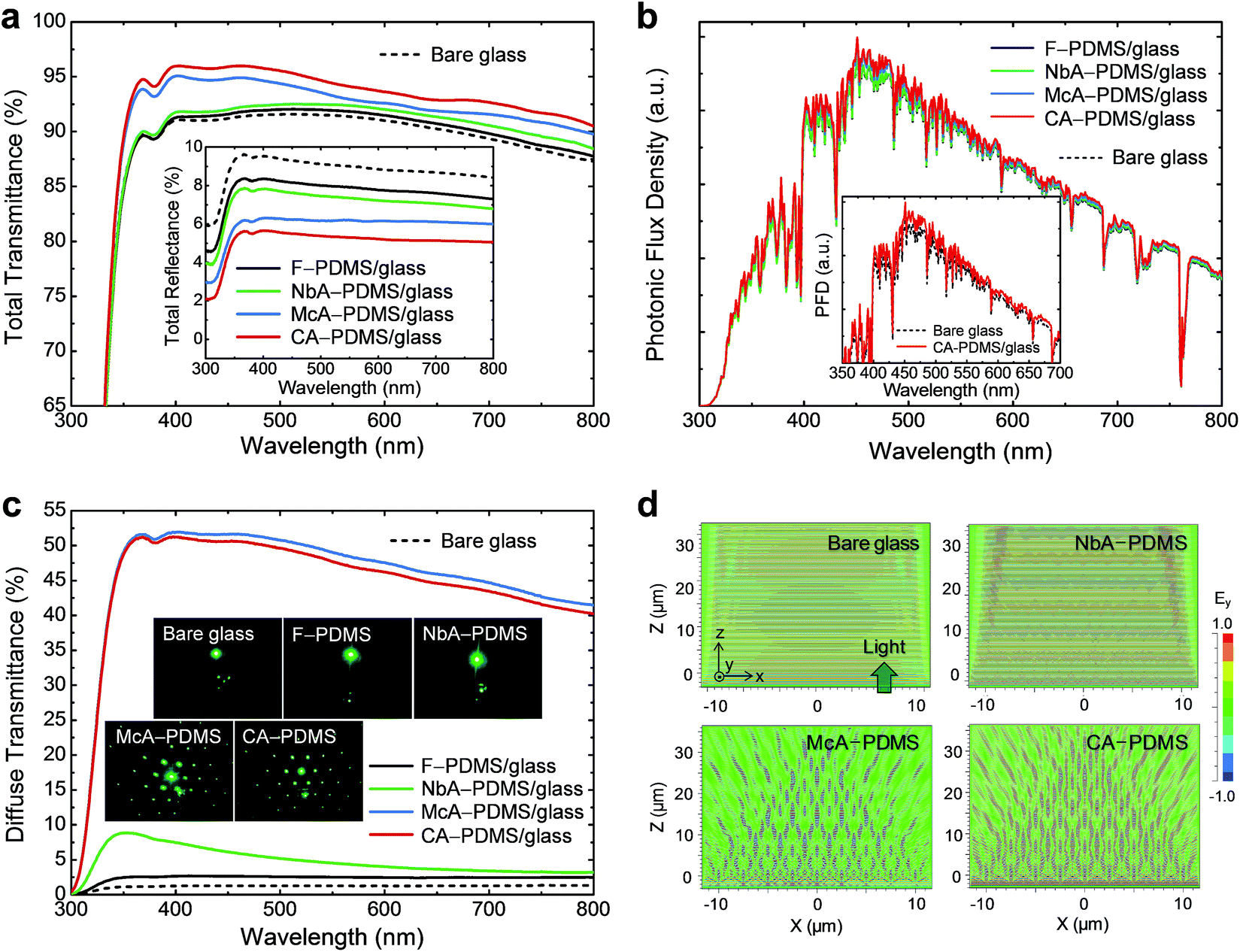 | ||
| Fig. 3 Measured (a) total and (c) diffuse transmittance spectra of bare glass, and the PDMS with different architectures (F-PDMS, NbA-PDMS, McA-PDMS, and CA-PDMS) including their measured total reflectance spectra in the inset of (a). (b) Spectral distributions of the PFD for their measured total transmittance spectra in (a) and (d) contour plots of the Ey distributions for the incident light propagating from the air to the corresponding structured PDMS at λ = 550 nm. Photographs of the corresponding samples for the verification of the light scattering properties are also shown in the inset of (c). | ||
These transmittance properties at specific wavelengths of the solar spectrum can be also observed using the calculation of the photonic flux density (PFD) which is the number of photons transmitted across the sample.51 Fig. 3(b) shows the spectral distributions of the PFD for the corresponding samples. Clearly, for CA-PDMS/glass, a larger PFD spectral distribution than those of the other samples is shown in the broad wavelength region of 350–800 nm, particularly at wavelengths of 450–550 nm, which is a range of high solar spectral photonic flux intensity. Compared with bare glass, it also exhibited a much higher PFD spectral distribution at wavelengths of 350–800 nm, as shown in the inset of Fig. 3(b). Therefore, it can be expected that an increase of photo-generated currents could be obtained from the cell absorption layer of DSSCs incorporated with CA-PDMS as a protective AR cover-layer of the glass, so it would lead to an efficiency enhancement of DSSCs.
When light enters into the grating structure with a period of P at normal incidence, the angle of the transmitted diffraction waves, θt,m, in the m-th diffraction order is given by the grating equation of sinθt,m = mλ/Pn,52 where λ is the incident wavelength of light and n is the refractive index of the incident medium. Therefore, the micro-periodic structures on transparent substrates such as glasses, polymers, etc., have a strong light scattering during transmissions. In addition, the haze ratio (H) is defined by the ratio of the diffuse transmittance (Td) to the total transmittance (Tt), i.e., H(%) = Td/Tt × 100. This H value indicates the light scattering property of a sample. In Fig. 3(c), the diffuse transmittance spectra of both McA-PDMS/glass and CA-PDMS/glass were much larger over a wide wavelength range of 350–800 nm due to their grating period of 2.9 μm while the other samples show almost no diffuse transmittance, exhibiting average H (HA) values of ∼51.4 and ∼49.7%, respectively (HA ≈ 1.4, 2.8, and 5.3% for bare glass, F-PDMS/glass, and NbA-PDMS/glass, respectively). This strong light scattering property of both McA-PDMS and CA-PDMS can also be confirmed from the photographs in the inset of Fig. 3(c). For flat bare glass, F-PDMS, and NbA-PDMS, there is almost no light diffraction, whereas McA-PDMS and CA-PDMS show a large diffracted light distribution at λ = 550 nm. Similarly, from the FDTD calculation in Fig. 3(d), McA-PDMS and CA-PDMS with a period of 2.9 μm exhibit a strong light scattering with a wide angular spread and help light to propagate across the interface between the air and the PDMS. For both flat bare glass and NbA-PDMS, there is no scattered light. From these results, it can be seen that this strong light scattering effect would positively improve the PCE of DSSCs.24–26
The influence of the PDMS with biomimetic architectures as a light-harvesting tool and a protective cover-layer of the outer glass surface on the device performance of DSSCs was studied. The J–V curves, the enhancement percentage of device characteristics relative to the reference DSSC, and the IPCE spectra for DSSCs with differently structured PDMS cover-layers are shown in Fig. 4(a–c), respectively. A schematic diagram and a photograph of the DSSC laminated with CA-PDMS are shown in the insets of Fig. 4(a) and (c), respectively. For comparison, the J–V curve and IPCE spectrum of the DSSC with bare glass as a reference device are also shown in Fig. 4(a) and (c), respectively. The device characteristics (open circuit voltage, VOC; short circuit current density, JSC; fill factor, FF; PCE) of the corresponding DSSCs are summarized in Table 1. The introduction of the patterned PDMS on the external surface of the glass substrate in the DSSCs improved the PCE. In particular, for the DSSC with CA-PDMS, a significantly increased PCE value of ∼8.24% was obtained compared to that (PCE ≈ 7.45%) for the reference DSSC, exhibiting a large PCE enhancement percentage of ∼10.7%. This is mainly due to the remarkable enhancement of the JSC value from ∼16.37 to ∼18.11 mA cm−2 rather than the VOC and FF, as can be seen in Table 1 and Fig. 4(b), because of the higher total transmittance (superior AR ability) and strong light scattering effect over a wide wavelength range of 350–800 nm. This confirms that the efficient light-harvesting layer can boost the light absorption in DSSCs, which produces improved photocurrents. On the other hand, for all the DSSCs, there is no distinct difference in both the VOC and FF. This indicates that the lamination of the PDMS layer does not affect the electrical and material properties of the DSSCs. The increased photocurrent can also be observed from the IPCE data (Fig. 4(c)). The DSSC with CA-PDMS showed a higher IPCE spectrum than those of the other DSSCs over the entire spectral range of 350–750 nm, indicating an average increment of ∼10% compared to the reference DSSC at the corresponding wavelengths. This value is similar to the JSC enhancement percentage of ∼10.6% in the J–V characteristics of Table 1.
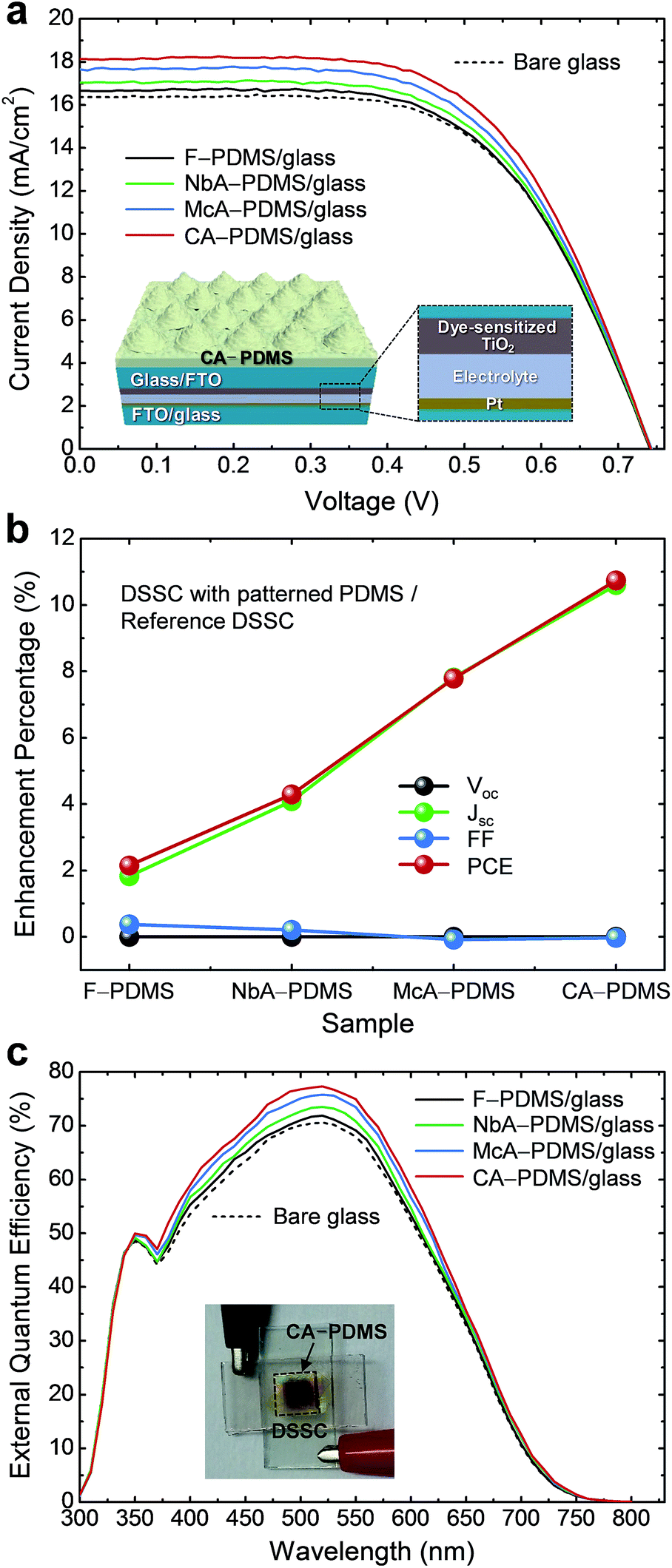 | ||
| Fig. 4 (a) J–V curves, (b) enhancement percentage of the device characteristics relative to the reference DSSC, and (c) IPCE spectra for DSSCs with differently structured PDMS cover-layers. A schematic diagram and a photograph of the DSSC laminated with CA-PDMS are shown in the insets of (a) and (c), respectively. | ||
| DSSCa | VOC [V] | JSC [mA cm−2] | FF [%] | PCE [%] |
|---|---|---|---|---|
| a For each DSSC, five devices or more were fabricated in the same fabrication facilities. All the DSSCs were characterized using a solar simulator under 1-sun AM1.5G illumination.b Mean value ± standard deviation. | ||||
| Bare | 0.742 ± 0.001b | 16.37 ± 0.21 | 61.33 ± 1.05 | 7.45 ± 0.02 |
| F-PDMS | 0.742 ± 0.001 | 16.67 ± 0.20 | 61.56 ± 1.00 | 7.61 ± 0.03 |
| NA-PDMS | 0.742 ± 0.001 | 17.04 ± 0.18 | 61.46 ± 1.02 | 7.77 ± 0.06 |
| MA-PDMS | 0.742 ± 0.001 | 17.65 ± 0.22 | 61.28 ± 1.01 | 8.00 ± 0.05 |
| CA-PDMS | 0.742 ± 0.001 | 18.11 ± 0.19 | 61.30 ± 1.06 | 8.24 ± 0.04 |
In outdoor environments, the dust particles and contaminants on the surface of solar cell systems are very harmful and degrade the device performance since they interfere with the incident light into the cell absorption layer. Therefore, a self-cleaning function at the top surface of solar cells is very useful to maintain the device performance.33,53 The water wetting behaviors of PDMS with differently structured surfaces were investigated as shown in Fig. 5. In the photographs of Fig. 5(a), the patterned PDMS showed higher water contact angle (θC) values compared to those of F-PDMS (θC ≈ 98°) as well as bare glass (θC ≈ 37°) (see Fig. S2(a) of the ESI†), indicating a hydrophobic surface. This is attributed to the increased surface roughness of PDMS explained by the Cassie and Baxter theory.54,55 In particular, CA-PDMS exhibited a larger θC value of ∼134° compared to those of NbA-PDMS (θC ≈ 104°) and McA-PDMS (θC ≈ 108°). The air is trapped in the interstices of the rough surface, and thus it can prevent the intrusion of water droplets into the nanobumps/microcones, resulting in the enhancement of the water contact angle on the more roughened surface of CA-PDMS. The dust and pollutants on the hydrophobic surface of CA-PDMS with θC ≈ 134° can be washed by rainwater droplets because it has relatively large dynamic advancing (θAC) and receding (θRC) water contact angle values of θAC ≈ 160° and θRCA ≈ 102° at the inclination angle of 40°, exhibiting a contact angle hysteresis (i.e., θAC − θRC) of ∼58° (see Fig. S2(b) in the ESI†). The self-cleaning behavior of CA-PDMS is observed in Fig. 5(b). When water droplets were dropped onto the surface of CA-PDMS covered with sand grains, the grains were clearly removed with rolling down water droplets without any sand and water droplets remaining at the surface. Thus, a protective cover-layer with an additional self-cleaning function like this CA-PDMS would enhance the practical feasibility of solar cells, displays, windows of buildings or cars, and various other optical components in real outdoor applications.
 | ||
| Fig. 5 (a) Photographs of a water droplet on the surface of NbA-PDMS, McA-PDMS, and CA-PDMS. (b) Sequential photographs of the water droplet cleaning behavior for CA-PDMS. | ||
Conclusions
PDMS with a biomimetic compound architecture consisting of hierarchical nanobumps/microcone arrays (i.e., CA-PDMS) was fabricated using a ICA-AAO mold by the SIL technique via the Mc-PSS. For CA-PDMS/glass, optical and surface wetting behaviors were investigated, together with theoretical analysis using the FDTD method. It exhibited much higher total and diffuse transmittance characteristics (TSW ≈ 94% and HA ≈ 49.7%) than those (TSW ≈ 90.4% and HA ≈ 1.4%) of bare glass in the broad wavelength range of 350–800 nm, and thus the surface reflection was reduced (RSW ≈ 5.3%). Furthermore, its self-cleaning effect (cf., θC ≈ 134° at the inclination angle of 0°, θAC ≈ 160° and θRC ≈ 102° at 40°) was also verified by the removal of sand grains by rolling down water droplets. For the DSSC with CA-PDMS as a protective light-harvesting cover-layer of the outer glass substrate, an improved PCE value of ∼8.24% was achieved by the enhanced photo-generated current of JSC ≈ 18.11 mA cm−2, indicating a significant PCE enhancement percentage of ∼10.7% compared to the reference DSSC with bare glass (PCE ≈ 7.45%, JSC ≈ 16.37 mA cm−2). These results can offer a deep understanding of biomimetic polymers with compound architectures, which can be easily realized by a simple and cost-effective SIL method via an AAO mold, with broadband light-harvesting and self-cleaning functions for high-efficiency DSSC device applications. Also, it is important to note that these CA-patterned polymers can be applied to various other solar cells and optical systems that use transparent substrates and covers such as glasses, plastics, sapphires, and quartzes.Acknowledgements
This work was supported by the National Research Foundation of Korea (NRF) grant funded by the Korea government (MSIP) (No. 2014-069441).References
- N. L. Panwar, S. C. Kaushik and S. Kothari, Renewable Sustainable Energy Rev., 2011, 15, 1513–1524 CrossRef PubMed.
- N. S. Lewis, Science, 2007, 315, 798–801 CrossRef CAS PubMed.
- M. E. Himmel, S. Y. Ding, D. K. Johnson, W. S. Adney, M. R. Nimlos, J. W. Brady and T. D. Foust, Science, 2007, 315, 804–807 CrossRef CAS PubMed.
- M. S. Dresselhaus and I. L. Thomas, Nature, 2001, 414, 332–337 CrossRef CAS PubMed.
- S. Mekhilef, R. Saidur and A. Safari, Renewable Sustainable Energy Rev., 2011, 15, 1777–1790 CrossRef PubMed.
- U. Bach, D. Lupo, P. Comte, J. E. Moser, F. Weissortel, J. Salbeck, H. Spreitzer and M. Gratzel, Nature, 1998, 395, 583–585 CrossRef CAS.
- A. Hagfeldt, G. Boschloo, L. Sun, L. Kloo and H. Pettersson, Chem. Rev., 2010, 110, 6595–6663 CrossRef CAS PubMed.
- N. Robertson, Angew. Chem., Int. Ed., 2006, 45, 2338–2345 CrossRef CAS PubMed.
- J. Lee and M. Lee, Adv. Energy Mater., 2014, 4, 1300978 Search PubMed.
- S. Colodrero, A. Mihi, L. Haggman, M. Ocana, G. Boschloo, A. Hagfeldt and H. Miguez, Adv. Mater., 2009, 21, 764–770 CrossRef CAS PubMed.
- K. Zhu, N. R. Neale, A. Miedaner and A. J. Frank, Nano Lett., 2007, 7, 69–74 CrossRef CAS PubMed.
- M. Pazoki, P. W. Lohse, N. Taghavinia, A. Hagfeldt and G. Boschloo, Phys. Chem. Chem. Phys., 2014, 16, 8503–8508 RSC.
- S. Ito, S. M. Zakeeruddin, R. H. Baker, P. Liska, R. Charvet, P. Comte, M. K. Nazeeruddin, P. Pechy, M. Takata, H. Miura, S. Uchida and M. Gratzel, Adv. Mater., 2006, 18, 1202–1205 CrossRef CAS PubMed.
- N. N. Zhang, B. Zhang, Y. H. Li, Y. Hou, S. Yang, J. H. Zhong and H. G. Yang, J. Mater. Chem. A, 2014, 2, 1641–1646 CAS.
- Y. M. Song, J. H. Jang, J. C. Lee, E. K. Kang and Y. T. Lee, Sol. Energy Mater. Sol. Cells, 2012, 101, 73–78 CrossRef CAS PubMed.
- H. K. Raut, S. S. Dinachali, Y. C. Loke, R. Ganesan, K. K. Ansah-Antwi, A. Gora, E. H. Khoo, V. A. Ganesh, M. S. M. Saifullah and S. Ramakrishna, ACS Nano, 2015, 9, 1305–1314 CrossRef CAS PubMed.
- Y. Nasuno, N. Kohama, K. Nishimura, T. Hayakawa, H. Taniguchi and M. Shimizu, Appl. Phys. Lett., 2006, 88, 071909 CrossRef PubMed.
- K. Choi, S. H. Park, Y. M. Song, Y. T. Lee, C. K. Hwangbo, H. Yang and H. S. Lee, Adv. Mater., 2010, 22, 3713–3718 CrossRef CAS PubMed.
- K. C. Park, H. J. Choi, C. H. Chang, R. E. Cohen, G. H. McKinley and G. Barbastathis, ACS Nano, 2012, 6, 3789–3799 CrossRef CAS PubMed.
- S. Y. Heo, J. K. Koh, G. Kang, S. H. Ahn, W. S. Chi, K. Kim and J. H. Kim, Adv. Energy Mater., 2014, 4, 1300632 Search PubMed.
- Q. Lin, S. F. Leung, L. Lu, X. Chen, Z. Chen, H. Tang, W. Su, D. Li and Z. Fan, ACS Nano, 2014, 8, 6484–6490 CrossRef CAS PubMed.
- Y. Liu, A. Das, S. Xu, Z. Lin, C. Xu, Z. L. Wang, A. Rohatgi and C. P. Wong, Adv. Energy Mater., 2012, 2, 47–51 CrossRef PubMed.
- J. W. Leem, J. S. Yu, D. H. Jun, J. Heo and W. K. Park, Sol. Energy Mater. Sol. Cells, 2014, 127, 43–49 CrossRef CAS PubMed.
- B. Janthong, Y. Moriya, A. Hongsingthong, P. Sichanugrist and M. Konagai, Sol. Energy Mater. Sol. Cells, 2013, 119, 209–213 CrossRef CAS PubMed.
- H. P. Wang, T. Y. Lin, M. L. Tsai, W. C. Tu, M. Y. Huang, C. W. Liu, Y. L. Chueh and J. H. He, ACS Nano, 2014, 8, 2959–2969 CrossRef CAS PubMed.
- C. H. Ho, D. H. Lien, H. C. Chang, C. A. Lin, C. F. Kang, M. K. Hsing, K. Y. Lai and J. H. He, Nanoscale, 2012, 4, 7346 RSC.
- J. W. Leem, M. S. Kim and J. S. Yu, J. Opt. Soc. Am. B, 2013, 30, 1665–1670 CrossRef CAS.
- Y. M. Song, G. C. Park, S. J. Jang, J. H. Ha, J. S. Yu and Y. T. Lee, Opt. Express, 2011, 19, A157–A165 CrossRef PubMed.
- J. W. Leem, Y. M. Song and J. S. Yu, Nanoscale, 2013, 5, 10455–10460 RSC.
- Y. H. Ko and J. S. Yu, Opt. Express, 2011, 19, 15574–15583 CrossRef CAS PubMed.
- W. Stork, N. Streibl, H. Haidner and P. Kipfer, Opt. Lett., 1991, 16, 1921–1923 CrossRef CAS.
- E. E. Perl, W. E. McMahon, R. M. Farrell, S. P. DenBaars, J. S. Speck and J. E. Bowers, Nano Lett., 2014, 14, 5960–5964 CrossRef CAS PubMed.
- Y. B. Park, H. Im, M. Im and Y. K. Choi, J. Mater. Chem., 2011, 21, 633–636 RSC.
- R. J. Martin-Plama, C. G. Pantano and A. Lakhtakia, Nanotechnology, 2008, 19, 355704 CrossRef PubMed.
- N. Koo, M. Bender, U. Plachetka, A. Funchs, T. Wahlbrink, J. Bolten and H. Kurz, Microelectron. Eng., 2007, 84, 904–908 CrossRef CAS PubMed.
- S. H. Lee, J. W. Leem and J. S. Yu, Opt. Express, 2013, 21, 29298–29303 CrossRef PubMed.
- S. H. Ahn and L. J. Guo, ACS Nano, 2009, 3, 2304–2310 CrossRef CAS PubMed.
- Y. M. Song, Y. Xie, V. Malyarchuk, J. Xiao, I. Jung, K. J. Choi, Z. Liu, H. Park, C. Lu, R. H. Kim, R. Li, K. B. Crozier, Y. Huang and J. A. Rogers, Nature, 2013, 497, 95–99 CrossRef CAS PubMed.
- T. W. Odom, J. C. Love, D. B. Wolfe, K. E. Paul and G. M. Whitesides, Langmuir, 2002, 18, 5314–5320 CrossRef CAS.
- S. Al-Maawali, J. E. Bemis, B. B. Akhremitchev, R. Leecharoen, B. G. Janesko and G. C. Walker, J. Phys. Chem. B, 2001, 105, 3965–3971 CrossRef CAS.
- C. Goh, K. M. Coakley and M. D. McGehee, Nano Lett., 2005, 5, 1545–1549 CrossRef CAS PubMed.
- F. Buyukserin, M. Aryal, J. Gao and W. Hu, Small, 2009, 5, 1632–1636 CrossRef CAS PubMed.
- F. Galeotti, F. Trespidi, G. Timo and M. Pasini, ACS Appl. Mater. Interfaces, 2014, 6, 5827–5834 CAS.
- D. H. Ko, J. R. Tumbleston, K. J. Henderson, L. E. Euliss, J. M. DeSimone, R. Lopez and E. T. Samulski, Soft Matter, 2011, 7, 6404–6407 RSC.
- J. W. Leem, X. Y. Guan, M. Choi and J. S. Yu, Sol. Energy Mater. Sol. Cells, 2015, 134, 45–53 CrossRef CAS PubMed.
- J. K. Hyun, C. Ahn, H. Kang, H. J. Kim, J. Park, K. H. Kim, C. W. Ahn, B. J. Kim and S. Jeon, Small, 2013, 9, 369–374 CrossRef CAS PubMed.
- Y. M. Song, H. J. Choi, J. S. Yu and Y. T. Lee, Opt. Express, 2010, 18, 13063–13071 CrossRef CAS PubMed.
- J. W. Leem, Y. Yeh and J. S. Yu, Opt. Express, 2012, 20, 4056–4066 CrossRef CAS PubMed.
- J. Zhao and M. A. Green, IEEE Trans. Electron Devices, 1991, 38, 1925–1934 CrossRef CAS.
- NREL’s Renewable Resource Data Center, retrieved 2014, http://rredc.nrel.gov/solar/spectra/am1.5.
- J. W. Leem and J. S. Yu, Mater. Sci. Eng., B, 2011, 176, 1207–1212 CrossRef CAS PubMed.
- E. Hecht, Optics, Addison Wesley, San Francisco, CA, 4th edn, 2002 Search PubMed.
- J. Son, S. Kundu, L. K. Verma, M. Sakhuja, A. J. Danner, C. S. Bhatia and H. Yang, Sol. Energy Mater. Sol. Cells, 2012, 98, 46–51 CrossRef CAS PubMed.
- A. B. D. Cassie and S. Baxter, Trans. Faraday Soc., 1994, 40, 546–551 RSC.
- A. D. Tserepi, M. E. Vlachopoulou and E. Gogolides, Nanotechnology, 2006, 17, 3977–3983 CrossRef CAS.
Footnotes |
| † Electronic supplementary information (ESI) available: SEM image of the Mc-PSS, wetting behavior of the bare glass and the F-PDMS, dynamic wetting behavior of the CA-PDMS at an inclination angle of 40°. See DOI: 10.1039/c5ra16276a |
| ‡ These authors contributed equally to this work. |
| This journal is © The Royal Society of Chemistry 2015 |