
 Open Access Article
 This Open Access Article is licensed under a
 Creative Commons Attribution 3.0 Unported Licence
Memory effect and coexistence of negative and positive photoconductivity in black phosphorus field effect transistor for neuromorphic vision sensors†
Arun
Kumar
 *a,
Kimberly
Intonti
ab,
Loredana
Viscardi
ab,
Ofelia
Durante
ab,
Aniello
Pelella
c,
Osamah
Kharsah
d,
Stephan
Sleziona
d,
Filippo
Giubileo
b,
Nadia
Martucciello
b,
Paolo
Ciambelli
e,
Marika
Schleberger
d and
Antonio
Di Bartolomeo
*ab
*a,
Kimberly
Intonti
ab,
Loredana
Viscardi
ab,
Ofelia
Durante
ab,
Aniello
Pelella
c,
Osamah
Kharsah
d,
Stephan
Sleziona
d,
Filippo
Giubileo
b,
Nadia
Martucciello
b,
Paolo
Ciambelli
e,
Marika
Schleberger
d and
Antonio
Di Bartolomeo
*ab
aDepartment of Physics ‘E.R. Caianiello’, University of Salerno, Via Giovanni Paolo II 132, Fisciano 84084, Italy. E-mail: akumar@unisa.it; adibartolomeo@unisa.it
bCNR-SPIN Salerno, Via Giovanni Paolo II 132, Fisciano 84084, Italy
cDepartment of Science and Technology, University of Sannio, Via de Sanctis, Benevento 82100, Italy
dFakultät für Physik and CENIDE, Universität Duisburg-Essen, Lotharstrasse 1, Duisburg D-47057, Germany
eNarrando Srl, Via Arcangelo Rotunno 43, Salerno 84134, Italy
First published on 4th March 2024
Abstract
Black phosphorus (BP) field-effect transistors with ultrathin channels exhibit unipolar p-type electrical conduction over a wide range of temperatures and pressures. Herein, we study a device that exhibits mobility up to 100 cm2 V−1 s−1 and a memory window up to 1.3 μA. Exposure to a supercontinuum white light source reveals that negative photoconductivity (NPC) and positive photoconductivity (PPC) coexist in the same device. Such behavior is attributed to the chemisorbed O2 molecules, with a minor role of physisorbed H2O molecules. The coexistence of NPC and PPC can be exploited in neuromorphic vision sensors, requiring the human eye retina to process the optical signals through alerting and protection (NPC), adaptation (PPC), followed by imaging and processing. Our results open new avenues for the use of BP and other two-dimentional (2D) semiconducting materials in transistors, memories, and neuromorphic vision sensors for advanced applications in robotics, self-driving cars, etc.
New conceptsTwo-dimensional black phosphorus on SiO2 dielectric enables back gate field effect transistor with mobility up to 100 cm2 V−1 s−1, gate tunable hysteresis and coexisting negative and positive photoconductivity. This work is the first report on the coexistence of negative and positive photoconductivity in two-dimensional black phosphorus transistors. The black phosphorus devices are demonstrated as memories at higher temperature and low pressure. More importantly, the negative and positive photoconductivity enable their use as a neuromorphic vision sensor, which can be employed for advanced applications in robotics, self-driving cars, etc. |
Introduction
The recent surge of interest in two-dimensional (2D) materials, such as transition metal dichalcogenides (TMDs)1–6 and single elemental materials,7 has enabled tremendous progress in a broad range of applications, such as electronics,8,9 optoelectronics,10,11 spintronics,12,13 non-volatile memories,14 and neuromorphic computing.15,16 In this regard, single elemental 2D materials, such as graphene,17–19 phosphorene,14,20 silicene,21,22 and others, have gained much attention due to their superior properties.7 Despite its remarkable mobility and flexibility, graphene lacks a bandgap, which poses a significant hindrance to its application in digital logic circuits and transistors.23 Overcoming this limitation by introducing a bandgap in graphene is a complex challenge that remains a current focus of research.24,25 As an alternative to graphene, black phosphorus (BP) is a van der Waals type semiconducting layered material with a direct band gap from 0.3 eV (bulk) to 2 eV (monolayer) dependent on the number of layers.20 Notably, BP demonstrates high mobility values of 1000 cm2 V−1 s−1 and 3900 cm2 V−1 s−1 at room temperature (RT) 20 and low temperatures,26 respectively. On the other hand, the mobility diminishes at higher temperatures, due to the dominant phonon scattering, following a power law, μeff ∼ T−α, where α is a positive number that can be measured experimentally.27However, a major challenge in the fabrication of devices based on BP lies in its instability under ambient conditions, primarily due to spontaneous surface oxidation.28 Studies indicate that oxidation is triggered by interactions with oxygen (O2), as water (H2O) alone does not appear to react with pristine BP, although it may catalyze O2 induced oxidation.29,30 While the interaction of pristine BP with H2O has been extensively explored, the study of the hydrophilicity of oxidized BP is limited to the effects of localized O2 atoms chemisorbed on the surface.29,31 Consequently, exposure of BP to air results in moisture absorption, leading to modifications in both physical and chemical properties31,32 and, ultimately, to the degradation of its electronic properties.33 Despite this, most of the prior research has focused solely on the impacts of environmental molecules adsorbed on pristine BP. However, detailed investigations on the effect of the adsorbed molecules on the functional properties of BP have not been carried out so far.
In the present work, we explore a BP ultrathin flake, cleaned with deionized H2O and acetone, as the channel of a back gate field effect transistor (FET). The output and transfer characteristics confirm the unipolar p-type conduction. The transfer characteristics show a large hysteresis that depends on the applied gate and drain voltages. We exploit this property to achieve a memory behavior at different temperatures and low pressures. At higher temperatures, the device exhibits a wider programming window, in comparison to RT. Furthermore, we investigate the photoconductivity of the device at various temperatures. The device shows the coexistence of negative photoconductivity (NPC) and positive photoconductivity (PPC), a behavior found also at higher temperatures. We attribute this phenomenon to the adsorption and desorption of chemisorbed O2 molecules over the BP surface. More importantly, we point out that such behavior corresponds to a neuromorphic vision sensor, as a human eye retina processes the optical signal through alerting and protection (NPC), and adaptation (PPC), followed by imaging and processing.
Experimental methods
Bulk BP was mechanically exfoliated by employing adhesive tape to peel off a small thin flake of BP. The tape with BP was pressed onto a 300 nm SiO2/Si substrate surface. A maskless photolithography process followed e-beam evaporation to deposit 10 nm Ni and resistive thermal evaporation to deposit 70 nm Au electrodes. Ni contacts were chosen because they yield lower contact resistance in comparison to other metals or alloys.34,35 To minimize any degradation due to moisture absorption, a poly(methyl methacrylate) PMMA capping layer (80 nm) was placed over the top of the BP thin flake by spin coating at 40 rotations per second for 60 s.36 Prior to transferring the substrate for electrical measurements, the device was kept in diluted acetone containing 50% deionized (DI) H2O for 5 minutes and then cleaned with isopropanol. Dispersion in H2O and unavoidable exposure to air during sample handling causes oxidation; H2O alone does not seem to react with pristine BP, however, it may act as a catalyst for O2 oxidation. This induces physiosorbed H2O and chemisorbed O2 on the BP channel surface. The fabricated BP device was back gated by the heavily doped p ++ Si substrate, contacted by a silver (Ag) paste. Atomic force microscopy (AFM) (Nanosurf AG) was used to measure the thickness of the BP flake.Electrical measurements were performed in the two-probe configuration using a Janis ST-500 probe station connected to a Keithley 4200 SCS (semiconductor characterization system), having a current and a voltage sensitivity of about 0.1 pA, and 2 μV, respectively. Electrical measurements were carried out at 2 and 10−5 mbar pressure, and different temperatures ranging from RT to 370 K. The substrate temperature was monitored using a Scientific Instruments Model 9700 temperature controller, and the chamber pressure was maintained using a Pfeiffer vacuum pump.
Results and discussion
Fig. 1a shows the optical image of the fabricated BP FET device with a PMMA capping layer, having a channel length and width of 10.5 μm and 9.4 μm, respectively, resulting in a BP channel area of about Σ = 100 μm2. Fig. 1b displays the device schematic with the circuit utilized for the back gate and source–drain biases, Vgs, and Vds. Fig. 1c and d show the AFM image of the BP flake and the corresponding height profile, which confirms that the BP flake is about 10 nm thick.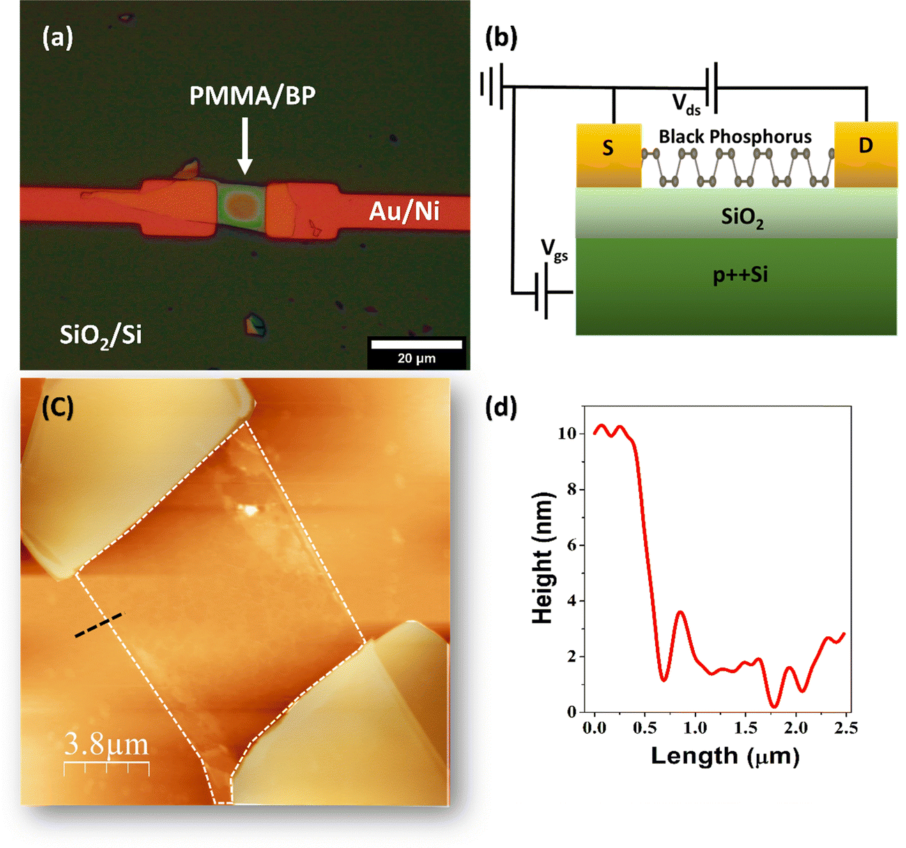 | ||
| Fig. 1 (a) Optical image of the BP FET device. (b) Schematic diagram of the BP FET device. (c) AFM image of the BP FET device. (d) Height profile along the black line over the BP channel. | ||
Initially, we conducted two-terminal transport measurements between the source and drain contacts at RT and 2 mbar pressure. In Fig. 2a, the output characteristics are shown, with the drain current (Id) plotted against the voltage drop across the two contacts (Vds), while the gate-source voltage (Vgs) serves as the control parameter. Notably, the device exhibits unipolar p-type conduction behavior, evident in the channel current increase under a negative applied gate voltage. The Id–Vds curves display linear behavior confirming ohmic contacts at any applied gate voltage.
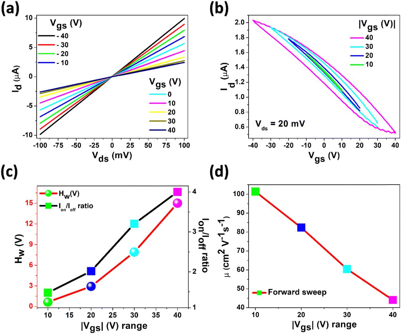 | ||
| Fig. 2 (a) Output, (b) transfer characteristics, (c) hysteresis width and on/off current ratio, and (d) calculated mobility as a function of the gate voltage at RT and 2 mbar pressure. Lines in (c) and (d) are guide to the eye. | ||
Fig. 2b illustrates the transfer characteristics of the device under a drain bias of 20 mV across varying loops of the gate voltage, covering the range of −40 V ≤ Vgs ≤ 40 V. We refrained from using higher gate voltages to prevent potential damage to the gate oxide. The observed transfer characteristics affirm the p-type behavior of the transistor, thereby validating that the Fermi level of the BP transistor fabricated with Ni contacts aligns closely with the valence band of the BP flake, and results in low contact resistance in comparison to other metals or alloys.34,35 We also observe that the transistor remains in the on-state at zero gate voltage, primarily due to the doping effect of the residual adsorbates, such as O2 and H2O molecules, as well as charges trapped at the BP/SiO2 interface which serve as p-dopants. Subsequently, we noted a minor modulation in the current and an increase in the hysteresis width, Hw, with an increasing sweeping range of Vgs. The limited current modulation is attributed to the low energy band gap of the multi-layer BP. We note that no pressure or strain was applied, which could otherwise enhance the band gap.37,38 Additionally, the applied gate electric field induces free carriers in the bottom layers of the BP flake, while the top layers could be relatively unaffected by the gate, thereby reducing the modulation in the drain current.39
Fig. 2c illustrates that the hysteresis width, defined as the difference in Vgs corresponding to the average current between the highest (Ion) and lowest (Ioff) currents at the extremes of the gate voltage range, increases with Vgs. The substantial hysteresis width, extending up to about 15 V, is attributed to trapped charges at the BP/SiO2 interface and intrinsic defects in BP. In Fig. 2c, the ratio of the on current to the off current (Ion/Ioff) is depicted, extracted from the transfer characteristics of the BP device across the investigated Vgs range. This highlights a current modulation factor of approximately 4. Our results of the Ion/Ioff ratio of around 4 are consistent with findings in the existing literature. The Ion/Ioff current depends directly on the thickness of the BP channel. F. Xia et al. investigated the dependence of BP based transistors on the thickness. They reported an exponentially decreasing on/off current ratio for BP flakes ranging from 2 to 17 nm.40 L. Feng et al. fabricated devices with BP flakes with a thickness ranging from 6 to 50 nm and studied the dependence of the transistor parameters on the BP channel thickness. They found a substantial increase in the drain current (several orders of magnitude) in devices fabricated with BP flakes ranging from 6 to 20 nm, while marginal increases were observed beyond 20 nm.41 Li et al. showed that the on/off current ratio of the BP transistor could reach up to 5 orders of magnitude when the thickness of the BP flake is less than 7.5 nm.20
The charge carrier mobility of the BP flake was determined through the utilization of the following equation:
In this equation, L = 10.5 μm, W = 9.4 μm, and Cox = 1.15 × 10⁻⁸ F cm−2 are the channel length, channel width, and gate oxide capacitance, respectively, while dId/dVgs is the maximum slope of the transfer curve.
Fig. 2d illustrates the two-terminal field-effect hole mobilities, showcasing the highest values of about 100 cm2 V−1 s−1 in the forward bias direction at Vds = 20 mV. The mobility and the sensitivity to Vgs are attributed to variations in the occupancy and behavior of interfacial trap states, exhibiting different characteristics during gate-voltage sweeps. The obtained mobility is comparable with the values reported in the literature for BP FET devices of similar thickness.42 Furthermore, it has been recently reported that the mobility of the carrier increases with the increase of the BP thickness.41 We have observed a similar trend of mobilities 100, 175, and 283 cm2 V−1 s−1 for exfoliated BP flakes with thicknesses of around 10, 20, and 30 nm, respectively.14,27
In Fig. 3a, the transfer curves of the BP device are depicted as a function of Vds, in the range from 10 to 100 mV. The recorded measurements reveal an absence of ambipolar behavior in the![[thin space (1/6-em)]](https://www.rsc.org/images/entities/char_2009.gif) ±40 V range, demonstrating instead strong unipolar p-type conduction behavior. Furthermore, the hysteresis width (Hw) was calculated as the change in current (μA) over the transfer characteristics at Vgs = 0 V. In Fig. 3b, it is observed that the hysteresis width increases with an increase in Vds. This trend suggests the influence of intrinsic traps within the BP channel, in addition to those at the BP/SiO2 interface, contributing to hysteresis generation. Indeed, the drain bias can affect the dynamics of intrinsic traps through the control of the channel current while the BP/SiO2 interface states and the traps in SiO2 dielectric are mainly controlled by the gate voltage. Higher current facilitates charge trapping in the channel, leading to a broader hysteresis. Fig. 3c illustrates that both Ion and Ioff currents exhibit a linear dependence on Vds, affirming the device operation in the linear (triode) region across the investigated Vgs and Vds ranges. Furthermore, the mobility reported in Fig. 3d, evaluated at Vgs ∼−40 V, increases with Vds and attains a maximum of about 48 cm2 V−1 s−1. The growing in-plane electric field increases the kinetic energy of charge carriers and makes the Coulomb scattering from trapped charges less effective.
±40 V range, demonstrating instead strong unipolar p-type conduction behavior. Furthermore, the hysteresis width (Hw) was calculated as the change in current (μA) over the transfer characteristics at Vgs = 0 V. In Fig. 3b, it is observed that the hysteresis width increases with an increase in Vds. This trend suggests the influence of intrinsic traps within the BP channel, in addition to those at the BP/SiO2 interface, contributing to hysteresis generation. Indeed, the drain bias can affect the dynamics of intrinsic traps through the control of the channel current while the BP/SiO2 interface states and the traps in SiO2 dielectric are mainly controlled by the gate voltage. Higher current facilitates charge trapping in the channel, leading to a broader hysteresis. Fig. 3c illustrates that both Ion and Ioff currents exhibit a linear dependence on Vds, affirming the device operation in the linear (triode) region across the investigated Vgs and Vds ranges. Furthermore, the mobility reported in Fig. 3d, evaluated at Vgs ∼−40 V, increases with Vds and attains a maximum of about 48 cm2 V−1 s−1. The growing in-plane electric field increases the kinetic energy of charge carriers and makes the Coulomb scattering from trapped charges less effective.
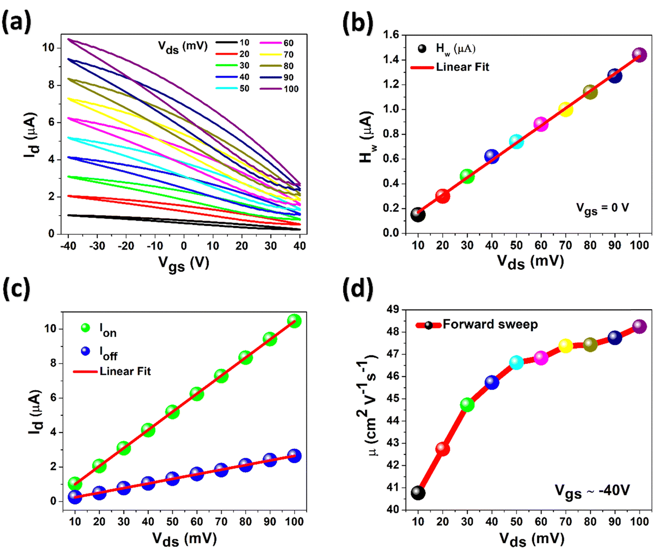 | ||
| Fig. 3 (a) Transfer characteristics, (b) hysteresis width, (c) on and off current values at Vgs = −40 V and Vgs = 40 V, respectively, and (d) calculated mobility as a function of the drain voltage at Vgs = −40 V, RT and 2 mbar pressure. Line in (d) is guide to the eye. | ||
In Fig. 4a and b, the transfer curves of the BP device are depicted at different temperatures, from RT to 370 K, at 2 mbar and 10−5 mbar, respectively. The recorded measurements reveal an absence of ambipolar behavior within the explored temperature range, instead a strong unipolar p-type conduction behavior is still maintained. However, a sawtooth-shape phenomenon was observed over the transfer curves at the explored range of temperatures. This could be due to the bubble/wrinkle formation over the BP surface resulting from dipping in H2O and interaction with O2.33,43 Wrinkles can lead to 2D material softening and affect their properties.44 Numerical simulations have shown that wrinkling in monolayer BP can lead to the sawtooth-shape phenomenon as a function of temperature due to shear deformation.45 The same phenomenon is noted in other 2D materials like graphene44 and MoS2.46 In Fig. 4c, it is observed that the hysteresis width increases with the rising temperature, both at 2 mbar and 10−5 mbar. This can be understood considering that the higher temperature facilitates the charge trapping processes at the BP/SiO2 interface, which leads to a wider hysteresis. The device shows a broader hysteresis at 2 mbar, in comparison to 10−5 mbar, as adsorbates still present on the BP surface can contribute to the phenomenon.29,47,48 Conversely, the higher Ion at 10−5 mbar likely results from an increase in mobility due to enhanced desorption of adsorbates at lower pressure. Furthermore, Fig. 4d illustrates the Ion/Ioff ratio with the increasing temperature, both at 2 mbar and 10−5 mbar. Remarkably, the Ion/Ioff ratio decreases with the rising temperature in both cases. Adsorbates such as H2O and O2 function as electron acceptors, leading to an increase in the p-type doping of the BP channel.49 The increasing temperature enhances the desorption of H2O and O2 molecules thus causing a decrease in the BP channel doping, which explains the decreasing Ion at higher temperatures. Fig. 4e illustrates the extracted mobility at 2 mbar and 10−5 mbar pressures as a function of increasing temperature. The highest recorded mobility was about 52 cm2 V−1 s−1 and 72 cm2 V−1 s−1 at 2 mbar and 10−5 mbar pressures, respectively. Notably, the observed behavior emphasizes that the modulation in the temperature influences the movement of charge carriers within the BP channel. The decrease in mobility at higher temperatures is due to phonon scattering, which constrains the hole transport. The results are consistent with the reported literature.27,50 The decreasing mobility follows a power law, μ ∼ T−α, where the exponent α depends on the dominant scattering mechanism, see Fig. 4f. The recorded exponent α ≈ 6–7 is consistent with the reported value for the explored range of temperatures.50
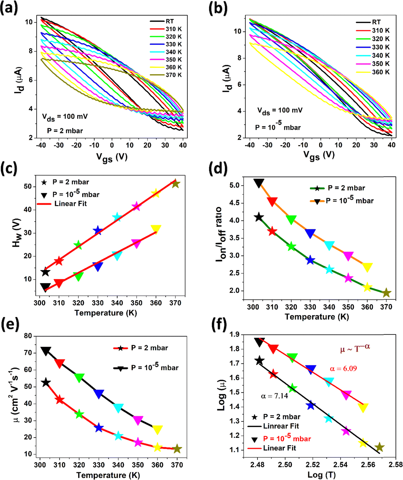 | ||
| Fig. 4 (a) and (b) Transfer characteristics, (c) hysteresis width, (d) on/off current ratio, (e) and (f) mobility at different temperatures of the BP device under 2 mbar and 10−5 mbar pressures. Lines in (d) and (e) are guide to the eye. | ||
In Fig. 5a, the memory response of the device in a SET/READ/RESET/READ sequence is depicted across various temperatures, at Vds = 100 mV and 2 mbar pressure. The current is observed throughout a sequence of Vgs = ±20 V RESET/SET pulses applied to the gate (for a longer time refer to ESI† Fig. S1a). Whether it is a positive or negative Vgs pulse, it establishes the current at a specific level, evolving over time and demonstrating consistent patterns at different temperatures. The persistence of the distinct current states, generated by positive and negative Vgs, extends more than 60 seconds, signifying a non-volatile characteristic of the BP FET. At zero gate voltage applied for memory READ purposes, the two currents following the RESET and SET states exhibit greater separation at higher temperatures, ranging from about 0.26 μA at 303 K to 1.3 μA at 370 K, with pressure at 2 mbar. This results in a broader memory window (ΔId) at higher temperatures, as depicted in Fig. 5b. Similarly, at a lower pressure (P = 10−5 mbar), Fig. 5c shows the separation of the currents after the RESET and the SET state, confirming larger separation with the increasing temperature, ranging from about 0.1 μA at 293 K to 0.8 μA at 360 K, at P = 10−5 mbar (refer to Fig. 5d; the memory behaviour for a longer time is reported in ESI† Fig. S1b). However, the memory window at 10−5 mbar pressure is lower in comparison to the memory performance at 2 mbar, due to a higher level of adsorbates in the latter case. The temperature-dependent memory window is ascribed to the temperature-enhanced trapping in the adsorbates and at the BP/SiO2 interface. Numerous defects formed at this interface act as deep intragap states, functioning as trap centers. These trap centers originate from BP intrinsic defects and processing residues at the BP/SiO2 interface. The gate voltage induces the storage of charge carriers in these trap centers, with trapping and de-trapping processes facilitated by higher temperatures. The transfer characteristic shape, exhibiting a right shift with an increasing Vgs sweeping range (see Fig. 4a and b), signifies the accumulation of the negative charge. During high positive or negative states of the gate pulse, the drain current undergoes a rapid increase or decrease, leading to the filling or emptying of intragap trap states by electrons, thereby causing the memory effect.
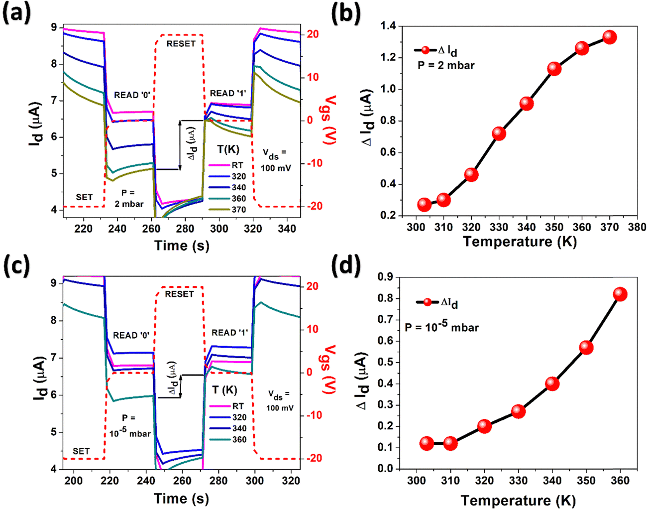 | ||
| Fig. 5 (a) and (b) SET/READ/RESET/READ cycles and memory window versus temperature under 2 mbar pressure. (c) and (d) SET/READ/RESET/READ cycles and memory window versus temperatures under 10−5 mbar pressure. Lines in (b) and (d) are guide to the eye. | ||
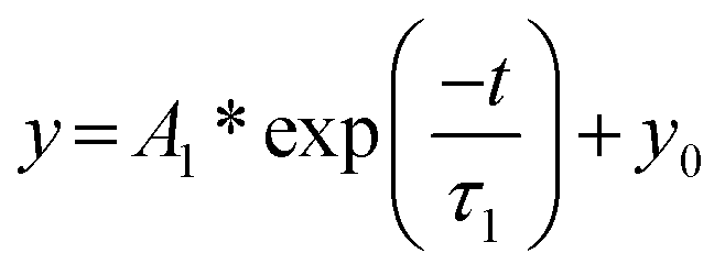
To explore the optoelectronic characteristics of BP, we examined the electrical conduction of the device by exposing to different light incident powers (the maximum laser power was 110 mW) at varying temperatures. The super-continuous light source was incident on the entire device, and toggled on and off at 4-minute intervals. The measurements were carried out at 10−5 mbar pressure; thus, the role of physiosorbed molecules (H2O) can be neglected, and the role of only chemisorbed molecules (such as O2) can be investigated to understand the optoelectronic mechanism. Fig. 6a illustrates the photocurrent as a function of time for different laser powers. The device shows the coexistence of NPC and PPC. Although the photocurrent periodic change at a 25% laser power is less evident, the NPC and PPC phenomena are pronounced well at higher laser powers. Fig. 6b shows the device channel current versus time under irradiation at different temperatures. Initially, the dark current is ≈4.91 μA (State I). When the light is turned on, the current suddenly decreases with a small step down, reaching a value of ≈4.88 μA (State II), showing NPC. Such a step is followed by a steady recovery and increase in current to a value of 4.94 μA (State III). At this point (State III), the laser is turned off, and it is observed that the current suddenly increases to 4.98 μA (State IV), and then slowly decreases without attaining its initial value (State V), following a long decay process (see ESI† Fig. S2). The process remained consistent across the entire temperature range under investigation. The presence of NPC at higher temperatures suggests the role of chemisorbed molecules (the physiosorbed molecules are mostly removed at high temperatures). Fig. 6c shows the time-resolved photocurrent under dark, illumination and dark conditions, at 310 K with maximum laser power. The photocurrent pulses can be fitted using a single exponential:
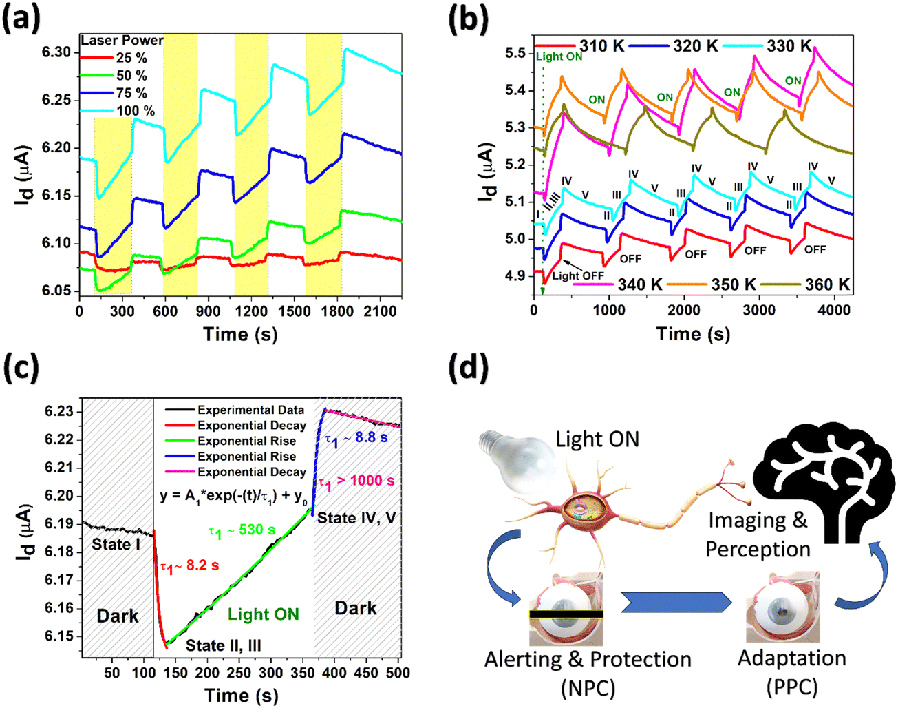 | ||
| Fig. 6 (a) Transient photocurrent at different laser powers at 310 K, Vds = 10 mV. (b) Transient photocurrent at different temperatures with a maximum laser power, at Vds = 100 mV. In both cases, the maximum laser power was 110 mW, 10−5 mbar pressure, and Vgs = 0 V. (c) Current decay/rise and exponential fit at 310 K, 10−5 mbar pressure. (d) Corresponding illustration of the obtained NPC and PPC for neuromorphic vision sensors. | ||
Finally, we highlight the potential of our device for use as a neuromorphic vision sensor. In the pursuit of enhancing machine vision capabilities, scientists are currently exploring advancements beyond the existing functional and imaging capacities of neuromorphic vision sensors. Specifically, in the realm of image recognition, researchers are working on refining neuromorphic vision sensors to incorporate advanced functionalities such as adaptive recognition, focus recognition, and selective focus reception.56 These features draw inspiration from the highly efficient visual recognition systems found in superior biological organisms.57,58Fig. 6d shows the human neuromorphic vision sensor behavior upon exposure to light. Immediate exposure to bright light initially overwhelms the human eye retina with dazzling effects (alerting and protection), which corresponds to the NPC response (State II) from the BP device. Followed by a light adaptation process of the human retina, it becomes possible to progressively recognize bright objects and that corresponds to the PPC response (State III) from the BP device. This process activates photosensitive cells and elevates the visual threshold for imaging and perception or recognition of objects in the human brain. Thus, based on the above correlation of the human neuromorphic vision process to the NPC and PPC over the semiconducting BP channel, we can say that the BP device has the potential to be applied in the field of artificial vision sensors. These sensors can be used to develop more efficient and intelligent vision systems for a wide range of applications, including robotics, self-driving cars, and medical imaging.
Conclusions
In summary, we fabricated an ultrathin BP FET with unipolar p-type conduction. The BP FET exhibits mobility up to 100 cm2 V−1 s−1. The transfer characteristics display hysteresis influenced by both the gate and drain bias, stemming from a combination of extrinsic and intrinsic trap states. This hysteresis has been exploited to achieve a memory device with a long retention time. The device shows a temperature-stable memory behavior with a wide programming window of 1.3 μA at higher temperatures. The memory window is found to be decreased at a lower pressure within the same explored temperature range. The device shows the coexistence of NPC and PPC under light illumination, even at high temperatures. We attributed NPC to the desorption of chemisorbed O2 molecules. We highlighted that the coexistence of NPC and PPC can be exploited for neuromorphic vision sensors. Our findings pave the way for investigating possibilities in various applications that demand semiconducting materials possessing a diverse array of properties. These applications encompass field-effect transistors, non-volatile memories, neuromorphic vision sensors, robotics, self-driving cars, etc.Conflicts of interest
There are no conflicts to declare.Acknowledgements
A. K. and A. D. B. acknowledge the European Union's REACT-EU PON Research and Innovation 2014–2020, Italian Ministerial Decree 1062/2021 Project. O. K., S. S., and M. S. acknowledge funding from the Deutsche Forschungsgemeinschaft (DFG, German Research Foundation) within the IRTG 2803 2D MATURE, project No. 461605777.References
- S. Manzeli, D. Ovchinnikov, D. Pasquier, O. V. Yazyev and A. Kis, Nat. Rev. Mater., 2017, 2, 1–15 CrossRef.
- W. Choi, N. Choudhary, G. H. Han, J. Park, D. Akinwande and Y. H. Lee, Mater. Today, 2017, 20, 116–130 CrossRef CAS.
- S. Joseph, J. Mohan, S. Lakshmy, S. Thomas, B. Chakraborty, S. Thomas and N. Kalarikkal, Mater. Chem. Phys., 2023, 297, 127332 CrossRef CAS.
- S. Tajik, Z. Dourandish, F. Garkani Nejad, H. Beitollahi, P. M. Jahani and A. Di Bartolomeo, Biosens. Bioelectron., 2022, 216, 114674 CrossRef CAS PubMed.
- M. B. Askari, P. Salarizadeh, P. Veisi, E. Samiei, H. Saeidfirozeh, M. T. Tourchi Moghadam and A. Di Bartolomeo, Micromachines, 2023, 14, 691 CrossRef PubMed.
- K. Intonti, E. Faella, A. Kumar, L. Viscardi, F. Giubileo, N. Martucciello, H. T. Lam, K. Anastasiou, M. Craciun, S. Russo and A. Di Bartolomeo, ACS Appl. Mater. Interfaces, 2023, 15, 50302–50311 CrossRef CAS PubMed.
- P. Vishnoi, K. Pramoda and C. N. R. Rao, ChemNanoMat, 2019, 5, 1062–1091 CrossRef CAS.
- S. Das, A. Sebastian, E. Pop, C. J. McClellan, A. D. Franklin, T. Grasser, T. Knobloch, Y. Illarionov, A. V. Penumatcha, J. Appenzeller, Z. Chen, W. Zhu, I. Asselberghs, L.-J. Li, U. E. Avci, N. Bhat, T. D. Anthopoulos and R. Singh, Nat. Electron., 2021, 4, 786–799 CrossRef CAS.
- O. Durante, K. Intonti, L. Viscardi, S. De Stefano, E. Faella, A. Kumar, A. Pelella, F. Romeo, F. Giubileo, M. S. G. Alghamdi, M. A. S. Alshehri, M. F. Craciun, S. Russo and A. Di Bartolomeo, ACS Appl. Nano Mater., 2023, 6, 21663–21670 CrossRef CAS PubMed.
- S. Lei, F. Wen, B. Li, Q. Wang, Y. Huang, Y. Gong, Y. He, P. Dong, J. Bellah, A. George, L. Ge, J. Lou, N. J. Halas, R. Vajtai and P. M. Ajayan, Nano Lett., 2015, 15, 259–265 CrossRef CAS PubMed.
- A. Kumar, E. Faella, O. Durante, F. Giubileo, A. Pelella, L. Viscardi, K. Intonti, S. Sleziona, M. Schleberger and A. Di Bartolomeo, J. Phys. Chem. Solids, 2023, 179, 111406 CrossRef CAS.
- N. R. Glavin, R. Rao, V. Varshney, E. Bianco, A. Apte, A. Roy, E. Ringe and P. M. Ajayan, Adv. Mater., 2020, 32, 1904302 CrossRef CAS PubMed.
- H. Li, S. Ruan and Y.-J. Zeng, Adv. Mater., 2019, 31, 1900065 CrossRef PubMed.
- A. Kumar, L. Viscardi, E. Faella, F. Giubileo, K. Intonti, A. Pelella, S. Sleziona, O. Kharsah, M. Schleberger and A. Di Bartolomeo, J. Mater. Sci., 2023, 58, 2689–2699 CrossRef CAS.
- G. Cao, P. Meng, J. Chen, H. Liu, R. Bian, C. Zhu, F. Liu and Z. Liu, Adv. Funct. Mater., 2021, 31, 2005443 CrossRef CAS.
- C. Feng, W. Wu, H. Liu, J. Wang, H. Wan, G. Ma and H. Wang, Nanomaterials, 2023, 13, 2720 CrossRef CAS PubMed.
- A. R. Urade, I. Lahiri and K. S. Suresh, JOM, 2023, 75, 614–630 CrossRef CAS PubMed.
- K. S. Novoselov, A. K. Geim, S. V. Morozov, D. Jiang, Y. Zhang, S. V. Dubonos, I. V. Grigorieva and A. A. Firsov, Science, 2004, 306, 666–669 CrossRef CAS PubMed.
- F. Urban, G. Lupina, A. Grillo, N. Martucciello and A. Di Bartolomeo, Nano Ex., 2020, 1, 010001 CrossRef.
- L. Li, Y. Yu, G. J. Ye, Q. Ge, X. Ou, H. Wu, D. Feng, X. H. Chen and Y. Zhang, Nat. Nanotechnol., 2014, 9, 372–377 CrossRef CAS PubMed.
- D. S. Dhungana, C. Grazianetti, C. Martella, S. Achilli, G. Fratesi and A. Molle, Adv. Funct. Mater., 2021, 31, 2102797 CrossRef CAS.
- C. Martella, C. Massetti, D. S. Dhungana, E. Bonera, C. Grazianetti and A. Molle, Adv. Mater., 2023, 35, 2211419 CrossRef CAS PubMed.
- G. Zhao, X. Li, M. Huang, Z. Zhen, Y. Zhong, Q. Chen, X. Zhao, Y. He, R. Hu, T. Yang, R. Zhang, C. Li, J. Kong, J.-B. Xu, R. S. Ruoff and H. Zhu, Chem. Soc. Rev., 2017, 46, 4417–4449 RSC.
- R. Nandee, M. A. Chowdhury, A. Shahid, N. Hossain and M. Rana, Results Eng., 2022, 15, 100474 CrossRef CAS.
- D. Dass, Diamond Relat. Mater., 2020, 110, 108131 CrossRef CAS.
- L. Li, G. J. Ye, V. Tran, R. Fei, G. Chen, H. Wang, J. Wang, K. Watanabe, T. Taniguchi, L. Yang, X. H. Chen and Y. Zhang, Nat. Nanotechnol., 2015, 10, 608–613 CrossRef CAS PubMed.
- A. Kumar, L. Viscardi, E. Faella, F. Giubileo, K. Intonti, A. Pelella, S. Sleziona, O. Kharsah, M. Schleberger and A. Di Bartolomeo, Nano Ex., 2023, 4, 014001 CrossRef.
- S.-L. Yau, T. P. Moffat, A. J. Bard, Z. Zhang and M. M. Lerner, Chem. Phys. Lett., 1992, 198, 383–388 CrossRef CAS.
- Y. Huang, J. Qiao, K. He, S. Bliznakov, E. Sutter, X. Chen, D. Luo, F. Meng, D. Su, J. Decker, W. Ji, R. S. Ruoff and P. Sutter, Chem. Mater., 2016, 28, 8330–8339 CrossRef CAS.
- J. Kumar and M. Shrivastava, ACS Omega, 2022, 7, 696–704 CrossRef CAS PubMed.
- A. Ziletti, A. Carvalho, D. K. Campbell, D. F. Coker and A. H. Castro Neto, Phys. Rev. Lett., 2015, 114, 046801 CrossRef CAS PubMed.
- F. Benini, N. Bassoli, P. Restuccia, M. Ferrario and M. C. Righi, Molecules, 2023, 28, 3570 CrossRef CAS PubMed.
- J. D. Wood, S. A. Wells, D. Jariwala, K.-S. Chen, E. Cho, V. K. Sangwan, X. Liu, L. J. Lauhon, T. J. Marks and M. C. Hersam, Nano Lett., 2014, 14, 6964–6970 CrossRef CAS PubMed.
- L. Viscardi, K. Intonti, A. Kumar, E. Faella, A. Pelella, F. Giubileo, S. Sleziona, O. Kharsah, M. Schleberger and A. Di Bartolomeo, Phys. Status Solidi B, 2023, 260, 2200537 CrossRef CAS.
- F. Telesio, G. le Gal, M. Serrano-Ruiz, F. Prescimone, S. Toffanin, M. Peruzzini and S. Heun, Nanotechnology, 2020, 31, 334002 CrossRef CAS PubMed.
- A. Kumar, L. Viscardi, E. Faella, F. Giubileo, K. Intonti, A. Pelella, O. Durante, S. Sleziona, M. Schleberger and A. D. Bartolomeo, in 2023 IEEE Nanotechnology Materials and Devices Conference (NMDC), 2023, 77–80.
- A. S. Rodin, A. Carvalho and A. H. Castro Neto, Phys. Rev. Lett., 2014, 112, 176801 CrossRef CAS PubMed.
- T. Fujii, Y. Nakai, Y. Akahama, K. Ueda and T. Mito, Phys. Rev. B, 2020, 101, 161408 CrossRef CAS.
- A. Grillo, A. Di Bartolomeo, F. Urban, M. Passacantando, J. M. Caridad, J. Sun and L. Camilli, ACS Appl. Mater. Interfaces, 2020, 12, 12998–13004 CrossRef CAS PubMed.
- F. Xia, H. Wang and Y. Jia, Nat. Commun., 2014, 5, 4458 CrossRef CAS PubMed.
- L. Feng, K. Liu and M. Wang, Appl. Sci., 2023, 13, 1736 CrossRef CAS.
- A. Grillo, A. Pelella, E. Faella, F. Giubileo, S. Sleziona, O. Kharsah, M. Schleberger and A. D. Bartolomeo, 2D Mater., 2021, 9, 015028 CrossRef.
- J. O. Island, G. A. Steele, H. S. J. van der Zant and A. Castellanos-Gomez, 2D Mater., 2015, 2, 011002 CrossRef.
- K. Min and N. R. Aluru, Appl. Phys. Lett., 2011, 98, 013113 CrossRef.
- Z. Yang, J. Zhao and N. Wei, Appl. Phys. Lett., 2015, 107, 023107 CrossRef.
- R. Zhang, Y. Lai, W. Chen, C. Teng, Y. Sun, L. Yang, J. Wang, B. Liu and H.-M. Cheng, ACS Nano, 2022, 16, 6309–6316 CrossRef CAS PubMed.
- F. Urban, F. Giubileo, A. Grillo, L. Iemmo, G. Luongo, M. Passacantando, T. Foller, L. Madauß, E. Pollmann, M. P. Geller, D. Oing, M. Schleberger and A. Di Bartolomeo, 2D Mater., 2019, 6, 045049 CrossRef CAS.
- A. Di Bartolomeo, A. Pelella, X. Liu, F. Miao, M. Passacantando, F. Giubileo, A. Grillo, L. Iemmo, F. Urban and S. Liang, Adv. Funct. Mater., 2019, 29, 1902483 CrossRef.
- A. Di Bartolomeo, A. Kumar, O. Durante, A. Sessa, E. Faella, L. Viscardi, K. Intonti, F. Giubileo, N. Martucciello, P. Romano, S. Sleziona and M. Schleberger, Mater. Today Nano, 2023, 24, 100382 CrossRef CAS.
- W. Liu, H. Zheng, K. Ang, H. Zhang, H. Liu, J. Han, W. Liu, Q. Sun, S. Ding and D. W. Zhang, Nanophotonics, 2020, 9, 2053–2062 CrossRef CAS.
- N. K. Tailor, C. A. Aranda, M. Saliba and S. Satapathi, ACS Mater. Lett., 2022, 4, 2298–2320 CrossRef CAS.
- A. Grillo, E. Faella, A. Pelella, F. Giubileo, L. Ansari, F. Gity, P. K. Hurley, N. McEvoy and A. Di Bartolomeo, Adv. Funct. Mater., 2021, 31, 2105722 CrossRef CAS.
- F. Urban, F. Gity, P. K. Hurley, N. McEvoy and A. Di Bartolomeo, Appl. Phys. Lett., 2020, 117, 193102 CrossRef CAS.
- E. Faella, K. Intonti, L. Viscardi, F. Giubileo, A. Kumar, H. T. Lam, K. Anastasiou, M. F. Craciun, S. Russo and A. Di Bartolomeo, Nanomaterials, 2022, 12, 1886 CrossRef CAS PubMed.
- K. Intonti, E. Faella, L. Viscardi, A. Kumar, O. Durante, F. Giubileo, M. Passacantando, H. T. Lam, K. Anastasiou, M. F. Craciun, S. Russo and A. Di Bartolomeo, Adv. Elect. Mater., 2023, 9, 2300066 CrossRef CAS.
- S. W. Cho, C. Jo, Y.-H. Kim and S. K. Park, Nano-Micro Lett., 2022, 14, 203 CrossRef CAS PubMed.
- G. J. Lee, C. Choi, D.-H. Kim and Y. M. Song, Adv. Funct. Mater., 2018, 28, 1705202 CrossRef.
- Z. He, D. Ye, L. Liu, C. Di and D. Zhu, Mater. Horiz., 2022, 9, 147–163 RSC.
Footnote |
| † Electronic supplementary information (ESI) available. See DOI: https://doi.org/10.1039/d4mh00027g |
| This journal is © The Royal Society of Chemistry 2024 |