
 Open Access Article
 This Open Access Article is licensed under a Creative Commons Attribution-Non Commercial 3.0 Unported Licence
Structure assembly regularities in vapour-deposited gold–fullerene mixture films
V.
Lavrentiev
*a,
M.
Motylenko
b,
M.
Barchuk
b,
C.
Schimpf
b,
I.
Lavrentieva
a,
J.
Pokorný
 c,
C.
Röder
d,
J.
Vacik
a,
A.
Dejneka
c and
D.
Rafaja
b
c,
C.
Röder
d,
J.
Vacik
a,
A.
Dejneka
c and
D.
Rafaja
b
aNS Lab, Nuclear Physics Institute CAS, Rez-130, Husinec 25068, Czech Republic. E-mail: lavrent@ujf.cas.cz
bInstitute of Materials Science, TU Bergakademie Freiberg, Gustav-Zeuner-Str. 5, D-09599 Freiberg, Germany
cInstitute of Physics CAS, Na Slovance 2, Prague 18221, Czech Republic
dInstitute of Theoretical Physics, TU Bergakademie Freiberg, Leipziger Str. 23, D-09599 Freiberg, Germany
First published on 25th February 2020
Abstract
Self-assembly is an attractive phenomenon that, with proper handling, can enable the production of sophisticated hybrid nanostructures with sub-nm-scale precision. The importance of this phenomenon is particularly notable in the fabrication of metal–organic nanomaterials as promising substances for spintronic devices. The exploitation of self-assembly in nanofabrication requires a comprehension of atomic processes creating hybrid nanostructures. Here, we focus on the self-assembly processes in the vapour-deposited AuxC60 mixture films, revealing the exciting quantum plasmon effects. Through a systematic characterization of the AuxC60 films carried out using structure-sensitive techniques, we have established correlations between the film nanostructure and the Au concentration, x. The analysis of these correlations designates the Au intercalation into the C60 lattice and the Au clustering as the basic processes of the nanostructure self-assembly in the mixture films, the efficiency of which strongly depends on x. The evaluation of this dependence for the AuxC60 composite nanostructures formed in a certain composition interval allows us to control the size of the Au clusters and the intercluster spacing by adjusting the Au concentration only. This study represents the self-assembled AuxC60 mixtures as quantum materials with electronic functions tuneable by the Au concentration in the depositing mixture.
A. Introduction
The present state of nanoscience designates metal–organic nanostructures (MONs) as an attractive subject, promising intriguing electronic effects in complex nanomaterials and assuming advanced applications.1–4 The great potential of such nanostructures refers, in particular, to the hidden opportunity of the electron-spin-related phenomena and the electronic flexibility of the metal–organic interface inherent to the MONs, for which proper understanding opens up wide prospects in future technologies.5–7 The use of C60 fullerene in MONs emphasises the material excellence due to the amazing features of the C60 molecules, such as exciting atomic structure and valuable electronic properties, intriguing coupling with metals, miniscule hyperfine interactions, enhanced structural stability, and rather low cost, which all together greatly enhance the interest in such materials.8,9Among the various C60-based MONs reported in the literature, the functional nanostructures of hybrid nanomaterials emerge through self-assembly; e.g., transition metal–fullerene (TM–C60) nanocomposites (NCs) fabricated by simultaneous deposition (SD) from vapour.10–13 The NC fabrication would enable proper control of the nanostructure, which promises a specific class of NC materials with tuneable electronic properties.14,15 The discovery of conductivity and superconductivity in alkali-metal fullerides was a strong motivation for the implementation of TM–fullerene-related research.16 The attempts to combine TM and C60 by the SD-method in order to access TM-fullerides usually revealed pronounced metal clustering, which strongly interfered with the main idea, but also supported the new functions of the emerging NC materials.17,18 A bright example of such materials is the SD-fabricated CoxC60 NC films, which have great potential in spintronics owing to the remarkable assembly of the magnetic Co clusters in the deposited mixture.19–21 This example argues the necessity to look inside the self-assembly in the TM–C60 mixture films in order to manage the material functions through controlling the nanostructure. Thus, in our recent work,15 we performed a systematic study of the cobalt–fullerene mixture films elucidating the atomic-scale mechanisms of the NC film self-assembly. Herein, we focus on the SD-fabricated Au–C60 mixed systems, whose intriguing plasmonic properties were recently discovered.22 The practical importance of this discovery motivated us to clarify the details of self-assembly in the AuxC60 mixture films by performing a systematic analysis of the nanostructures formed in such mixed systems. Success in the realization of this task would allow, for instance, the management of the discovered plasmonic effects, which promises new applications of TM–C60 NC materials. To date, the information on the structure and properties of the AuxC60 mixture films is still insufficient for discussing self-assembly effects (see, for instance, ref. 23).
B. Experimental
We fabricated a set of the AuxC60 mixture films (0 < x < 30) by means of the simultaneous deposition of Au and C60 from vapour onto the Si(100) substrates under vacuum at 10−6 mbar, as previously described elsewhere.22 The Au pellets (99.99 mass% Au) were evaporated using an electron gun operated by a digital power supplier (FuG Elektronik GmbH). The evaporation of C60 (99.9 mass% C60) was carried out by means of a Knudsen cell-like source. The Si(100) substrate was kept at 100 °C during the deposition of the films. For proper comparison of the deposited samples, pure C60 film was also prepared under the same conditions but the electron gun used for the Au supply was closed by a shutter. The Au concentration in the AuxC60 mixture films was controlled by the adjustment of the Au deposition rate using a quartz thickness monitor. The deposition rate of C60 was kept constant. The thickness of the deposited films was varied in the range of 120–200 nm.The precise chemical composition and thickness of the deposited mixture films were verified by the high-resolution Rutherford backscattering spectrometry (RBS) using a 2 meV He+ ion beam. The RBS experiments were carried out under vacuum at 10−7 mbar; the sample holder was kept at room temperature (RT). The analysing ion beam was provided by the 3 MV accelerator Tandetron 4130 MC (HVE). The RBS spectra were converted into the respective depth profiles of the chemical elements using a SIMNRA computer code.24
The surface morphologies of the deposited AuxC60 mixture films were analysed by the atomic force microscopy (AFM) using a modular scanning probe microscope NTEGRA-Aura (NT-MDT Spectrum Instruments). The AFM experiments were realized using the tapping mode and by exploiting the NSG03 AFM probes,15 keeping the samples under ambient atmospheric conditions.
The nanostructure and the phase composition of the deposited AuxC60 mixture films were analysed using high-resolution transmission electron microscopy (HRTEM), selected area electron diffraction (SAED) in transmission electron microscopy (TEM) and by X-ray diffraction (XRD). The size distribution and average size of the Au clusters were obtained from the analysis of approximately 250 particles per sample. Select Au clusters were investigated in greater detail in order to explore their internal structures. HRTEM analyses were performed using a high-resolution analytical transmission electron microscope JEM-2200FS (JEOL) that was operated at an accelerating voltage of 200 kV. The microscope was equipped with a field emission gun and an energy-dispersive X-ray (EDX) detector JED-2300 from JEOL. The TEM specimens of the AuxC60 films were prepared using the Precision Ion Polishing System (PIPS II) from Gatan.
The XRD patterns were recorded with a Bruker D8 Advance diffractometer. The diffractometer was equipped with a sealed X-ray tube with a Cu anode, a Ni/C Goebel mirror in the primary beam, a horizontal Soller collimator and a LiF monochromator located in the diffracted beam. The X-ray tube was operated at 40 kV and 40 mA. The combination of the Soller collimator with the acceptance angle of 0.12° and the LiF monochromator allowed us to eliminate unwanted radiation components and reduced the Kα2/Kα1 intensity ratio to 0.12. The XRD measurements were carried out in asymmetric diffraction geometry with a fixed angle of incidence of 2°. The diffraction angle (2θ) was varied from 5° to 75°. The step size was set at 0.05° 2θ with the counting time of 60 s per step. The applied small angle of incidence greatly reduced the penetration depth of the primary beam into the sample and enhanced the intensities diffracted by the thin films.
Raman spectra were recorded using the Renishaw InVia spectrometer supplied with a 514.5 nm laser. In order to avoid damage to the film structure under the laser irradiation, the beam intensity was properly reduced and the acquisition time was minimized.15 The setup parameters during the Raman experiments were optimized by testing the standard C60 films deposited on Si(100). The obtained Raman spectra were verified by using a LabRam HR800 Raman spectrometer (Horiba Jobin Yvon) with the laser wavelength of 532 nm. To avoid laser-induced degradation of the samples, the laser power density was also carefully adjusted by the filters.
C. Results
C1 RBS results: chemical composition of the mixture films
A reliable analysis of the chemical composition of the deposited mixture films is a crucial point in the present research, as it is essential for understanding the structural assembly in AuxC60 samples.15 The use of improper methods, such as the estimation of the film thickness,20,21 can involve large errors that could strongly affect the correctness of the modelling of the film structure formation. RBS has an evident advantage in this case as it is a non-destructive and high-resolution technique for the characterization of thin films with complex compositions.25 This technique is quite appropriate for the analysis of the metal–fullerene mixture films.15,22Fig. 1a demonstrates a series of RBS spectra recorded from the deposited mixture films with increasing Au content. Fig. 1b shows the experimental and simulated RBS spectra corresponding to the selected AuxC60 samples with Au concentrations x = 3.3, x = 9.4 and x = 16.3, which we call S2, S5 and S8, respectively. Fig. 1c summarizes the depth profiles of the elements in these samples obtained from the SIMNRA simulations.24 We selected these samples for farther comparison of RBS and TEM results.
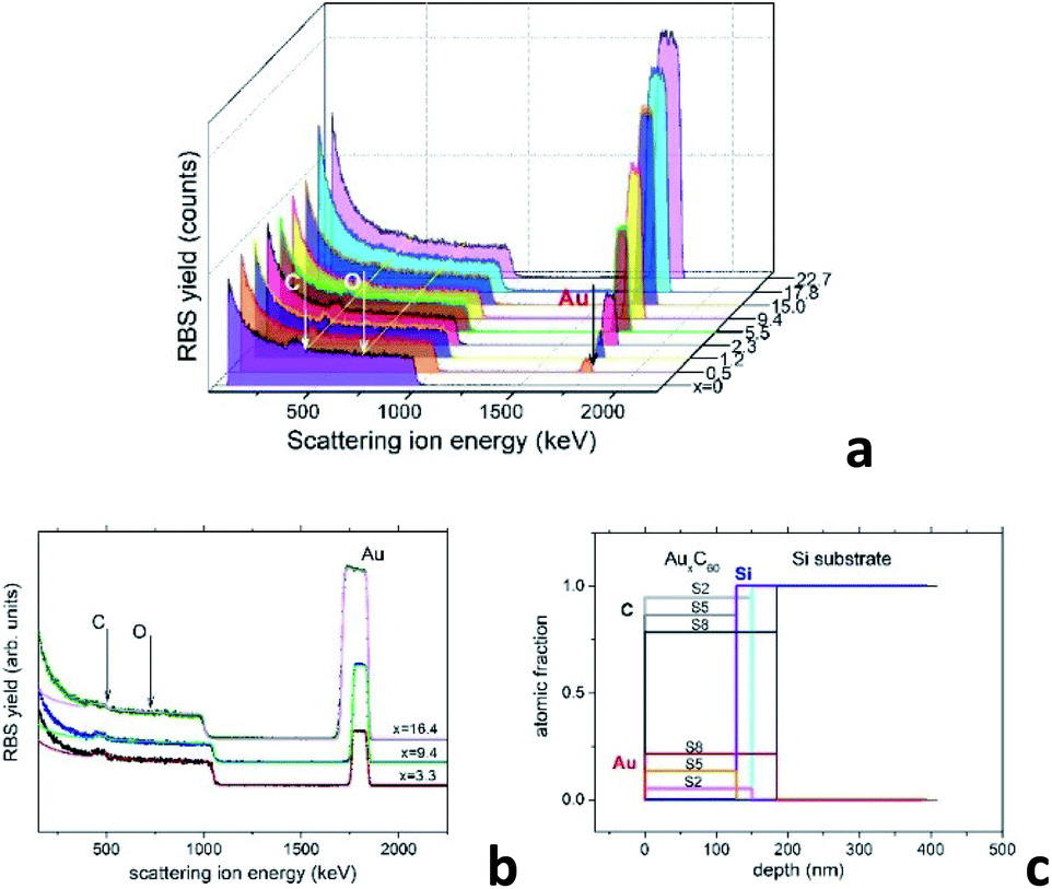 | ||
| Fig. 1 (a) RBS spectra of the AuxC60 mixture films with gradually increasing Au content. The thin yellow lines and the white vertical arrows indicate the energies corresponding to C and O at the film surface. The energy position of Au at the sample surface is indicated by the black arrow. The coloured plateau corresponds to the response of the Si substrate. (b) Experimental (dots) and simulated (solid lines) RBS spectra of samples S2 (x = 3.3), S5 (x = 9.4) and S8 (x = 16.4). (c) Depth profiles of chemical elements in the samples S2, S5 and S8 determined using the SIMNRA code.24 | ||
As one can see, the RBS spectra revealed only two elements in the mixture films, namely Au and C. Their existence is confirmed by the respective peaks appearing in the spectra nearby 504 keV and 1844 keV (see Fig. 1a and b). In contrast to CoxC60 films,15 the presence of oxygen in the AuxC60 films was not detected by RBS, although the films were exposed to air for about 0.5 h, before the RBS experiments. As seen from Fig. 1a and b, there is no peak visible at the expected O-related position near 726 keV. The edge at around 1000 keV and the increased RBS yield below this edge represent the RBS response of the Si substrate. The concentrations of Au and C in the films are proportional to the respective RBS yield. It is worth noting, the RBS yields are determined by the (strongly different) ion scattering cross-sections of Au and C,25 thus the RBS response from Au is much stronger than the RBS response from carbon. The simulation of the RBS spectra using the SIMNRA code24 revealed a uniform distribution of Au (and C) in the deposited films (see Fig. 1c). Using RBS results, we identify the chemical composition of the mixture films by formula AuxC60, where x corresponds to the number of Au atoms per one C60 molecule.15
C2 AFM results: surface morphology of the mixture films
Valuable information about the film nanostructure can be obtained from the AFM analysis of the surface morphology. Indeed, our recent study of the CoxC60 mixture films15 shows that surface morphology of the mixture films can be strongly influenced by the structural transformations occurring in the bulk of material during the film structure assembly. It was assumed that self-assembly in the AuxC60 mixture films will also influence the film surface morphology in a regular way during gradual increase of the Au concentration in the film. Thus, Fig. 2a demonstrates the selected AFM images of the AuxC60 films with various Au concentrations x. There are clear changes in the mixture film surface morphology when x increases from x = 0 to x = 22.7 (see Fig. 2a). In order to specify some details of structure self-assembly, it is convenient to consider these changes together with comparison of the surface roughness in the films with different x.15 Thus, variation of the root-mean-square (RMS) surface roughness (Rrms), taking place during the increase in the Au concentration x in the mixture films, is shown in Fig. 2b.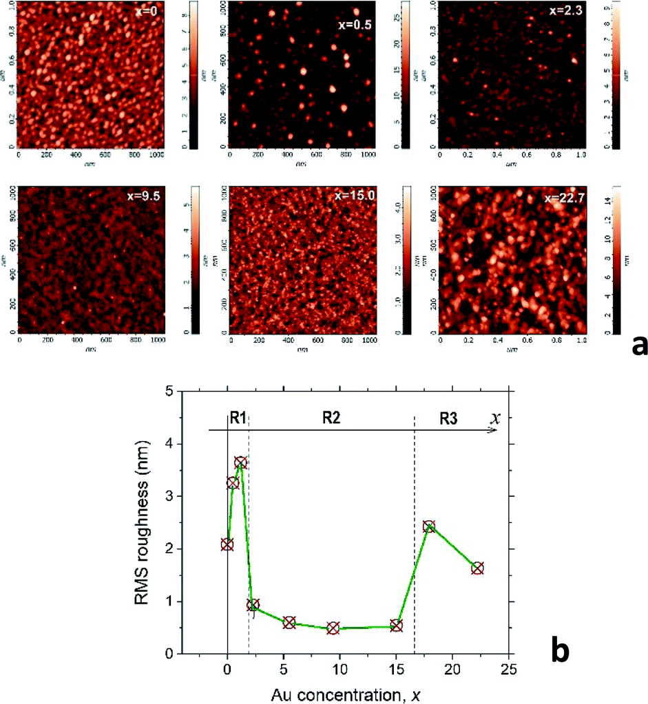 | ||
| Fig. 2 (a) AFM images of the surface morphology of selected AuxC60 films. The Au concentrations x in the films were added to the respective images. (b) Variation of the RMS surface roughness of the AuxC60 films with increasing x. R1, R2 and R3 indicate three different x intervals in which the AuxC60 nanostructures possess a common structural feature. Vertical dashed lines indicate the border (critical points, xc) between the intervals (see text). | ||
From Fig. 2b, it follows that the Rrms(x) dependence is a non-monotonic curve with critical points (critical concentrations, xc), which are the points where the curve shows a dramatic change in Rrms.15 Such a definition of the critical points allows us to distinguish three concentration intervals that designate three respective groups of the mixture films with common structural features. The first critical point, xc1, was estimated roughly as xc1 ≈ 1.7 ± 0.5 (the uncertainty is defined by a value of the x-step across the point xc1), which designates the interval R1 as 0 < x < xc1 in which the Rrms roughness shows some growth with increasing x, reaching the maximum value of 3.7 nm (the Rrms of pure C60 film was found to be about 2.0 nm). The surface of the mixture films related to this interval of x includes the irregular hillocks (see Fig. 2a, white spots in the AFM image of the film with x = 0.5). If x > xc1, the Rrms roughness drops rapidly to values below 1 nm and stays nearly constant within the broad interval of x (see Fig. 2b). This feature of the Rrms(x) dependence designates the second specific interval of x (interval R2), which can be described as xc1 < x < xc2 (xc2 ≈ 16.4 ± 1.4). The AuxC60 films related to this x interval possess a rather smooth surface as compared with that in the films from interval R1 (see the AFM images in Fig. 2a). The roughness of the films with x > xc2 suddenly increased, reaching almost 2 nm at higher x (see Fig. 2b). This Rrms effect is reflected by the respective AFM image of the film with x = 22.7, where a rough surface is clearly seen (see Fig. 2a). We call R3 the interval of x > xc2, while the point of xc2 is a second critical point.
Taking into account our results obtained for the CoxC60 mixture films15 and the recent discovery of quantum plasmon in the AuxC60 mixture films,22 we could relate the R2 interval with the films, in which the structure assembly leads to the formation of Au clusters. In order to verify this assumption, we performed TEM studies on AuxC60 films.
C3 TEM results: Au clustering and composite nanostructure
Fig. 3a (the upper row) shows the TEM cross-section images of samples S2, S5 and S8. The thicknesses of these AuxC60 mixture films (marked by green lines with arrows in Fig. 3a) correlate nicely with the values from the RBS spectra (cf. the depth profiles in Fig. 1c). The heterogeneity of the film structure on the nanoscale is clearly seen as the numerous black dots uniformly distributed in the whitish matrix. Taking into account the Z-contrast stemming from the different atomic numbers of gold and carbon, we can assign the black dots to Au clusters (or small Au nanoparticles, NPs) and the whitish matrix to carbon (or C60). The SAED analysis of the samples (bottom row in Fig. 3a) confirmed that Au NPs possess a face-centred cubic (fcc) crystal structure. The transition from continuous diffraction rings in sample S2 to distinct diffraction spots in sample S8 indicates the increase in the Au NP size with increasing Au concentration. This finding was confirmed by a detailed analysis of the SAED patterns (Fig. 3b), which revealed that the diffraction lines became narrower as the Au NPs became larger with increasing x. No preferred orientation of the Au NPs was detected.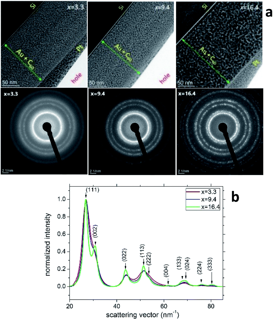 | ||
| Fig. 3 (a) TEM images (top row) and SAED patterns (bottom row) taken from the samples S2, S5 and S8 of the AuxC60 mixture films with Au concentrations of x = 3.3, x = 9.4 and x = 16.4, respectively. The SAED patterns were obtained from circular areas of the samples having a diameter of about 100 nm. (b) Radial intensity distribution in samples S2, S5 and S8 obtained using the “ProcessDiffraction” software26,27 from the SAED patterns. The intensities were normalized to the intensity of the respective (111) reflections. | ||
Characterization of the AuxC60 film nanostructure using HRTEM is presented in Fig. 4. The analysis of the HRTEM images of the mixture samples (Fig. 4a) yielded detailed information on the film nanostructure and size of the Au NPs in the AuxC60 mixture films. In the HRTEM micrographs, the Au NPs appear as black round spots with sizes of a few nm. On increasing the Au concentration, the size of the Au NPs clearly increased and the size distribution became broader (Fig. 4b). The average size of the Au NPs formed in sample S2 (x = 3.3) was (3.4 ± 0.35) nm, (4.2 ± 0.60) nm in sample S5 (x = 9.4) and (7.96 ± 1.12) nm in sample S8 (x = 16.4). The detailed inspection of the HRTEM images revealed the lattice contrast (the Au NPs selected by yellow squares in Fig. 4a) that allowed us to suppose the single-crystalline origin of the Au NPs.
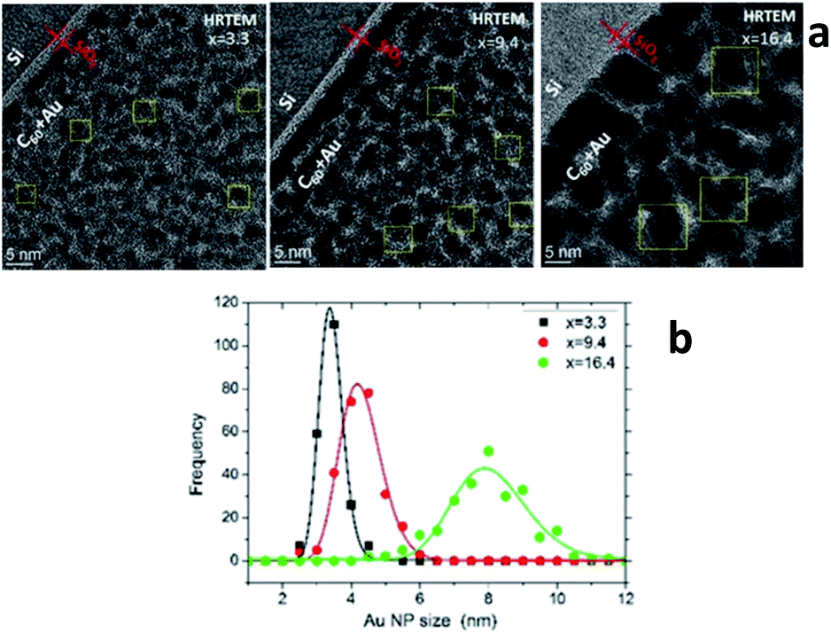 | ||
| Fig. 4 (a) HRTEM images of samples S2, S5 and S8. The whitish strip between the Si substrate and AuxC60 mixture film corresponds to native SiO2 layer (about 2 nm in thickness). (b) Log-normal size distribution of the Au NPs in samples S2, S5 and S8 as obtained from the analysis of approximately 250 NPs per sample. | ||
Using the concept of the composition intervals introduced above, the AuxC60 mixture samples S2, S5 and S8 can be attributed principally to the R2 interval. According to the AFM results (Fig. 2b), this x interval ranges between 1.7 and 16.4. According to TEM, the Au NPs, which were produced in this composition interval, have sizes between 2 nm and 10 nm (Fig. 4b). Taking this attribute into account and the evaluated dependence of the Au NPs size on x, we found that in the interval R2, the nucleation and growth of separated Au clusters constituted the main mechanisms of the nanostructure self-assembly in the mixture AuxC60 films (see Fig. 4). Sample S8 (x = 16.4) terminates the R2 interval (the S8 composition corresponds to the critical point xc2, see Fig. 2b). As the definition of xc (see the previous section) allows for some uncertainty, the nanostructure of sample S8 can include structural features from the neighbouring x interval that can allow us to also specify the neighbouring interval R3 using sample S8.
According to the HRTEM analysis (Fig. 4a), most Au NPs in sample S8 are in direct contact. Thus, a greater increase in the Au content in the mixture caused the coalescence and merging of the neighbouring NPs. The coalescence of the Au NPs is demonstrated by the HRTEM image displayed in Fig. 5. The NP coalescence of two Au nanoparticles (a smaller one and a larger one) results in the formation of a (111) twin boundary between the NPs and also causes twinning inside the merged NPs.28,29 The coalescence of NPs in the form of twins reduces the total energy of the system. Twinning inside the NPs is a result of the relaxation of the internal stress that arises from the touching of the growing NPs. It is worth noting that twinning is a common phenomenon in small metallic NPs, which has been actively studied in the last decade.30–32 This interesting problem is out of the framework of the present study and will be considered in a subsequent publication.
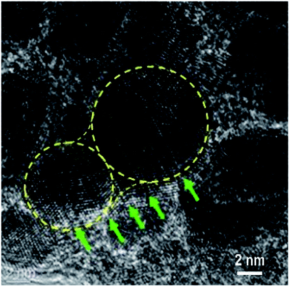 | ||
| Fig. 5 HRTEM image of nanostructures at the edge of the sample S8 (x = 16.4). The Au NP with irregular shape seen in the centre of the image is a coalescence of two NPs with different sizes. The crystal twinning in the Au NPs is seen. The position of the {111} twin boundaries in the Au NPs is indicated by green arrows. The crystal lattice in the Au NPs is well observed as the (111) plane in the twinned crystals. | ||
The TEM experiments helped us to understand the formation of Au NPs and the formation of planar defects in larger NPs but they did not allow us to properly analyse the C60-based matrix of the AuxC60 nanocomposites (because of C60 destruction during the TEM experiments). The matrix phase was characterized using XRD and Raman spectroscopy. The results of these techniques are presented in the next sections.
C4 XRD results: Au and C60 nanocrystals in the mixture films
The XRD experiments confirmed the presence of fcc Au NPs in all AuxC60 samples under study and revealed that carbon is present in the form of fcc-C60.15,33,34 Still, one can see from the XRD patterns displayed in Fig. 6 that the structural quality of fcc-C60 is different in individual samples. It was the highest in the undoped C60 film (x = 0), where pronounced diffraction lines 111, 220 and 311 were observed (Fig. 6), and decreased with increasing Au content in AuxC60. The degradation of the structural quality of fcc-C60 at higher Au concentrations is visible from the diffraction line broadening, which was caused by the reduction of the crystallite size, and from the reduction of the diffraction line intensities at higher diffraction angles. This was caused by the increasing displacement of the C60 molecules from their ideal positions in the fcc crystal structure, which is often described in terms of the static Debye–Waller factor.35 It is worth noting that similar changes in the diffraction pattern from fcc-C60 were also detected in the CoxC60 mixture films.15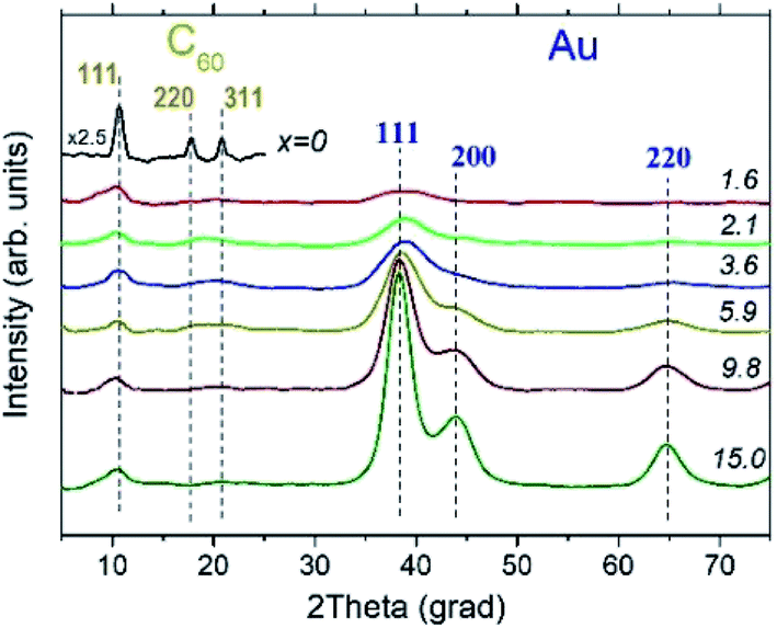 | ||
| Fig. 6 XRD patterns of pure C60 film (x = 0) and of AuxC60 mixture films with different Au contents (x). The x values are shown in the plots. Experimental XRD patterns were smoothed prior to plotting, and the rapidly increasing background at smaller angles was subtracted. | ||
Individual XRD lines from fcc-Au were fitted with the Gaussian distribution36 to obtain the line positions and line broadening for further analyses. Line broadening was employed to alternatively estimate the crystallite size using the Scherrer equation37
(B![[thin space (1/6-em)]](https://www.rsc.org/images/entities/char_2009.gif) cosθ)/λ = K/L cosθ)/λ = K/L | (1) |
Eqn (1) describes the relationship between the XRD peak half-width (B) and the crystallite size (L). The factor cosθ/λ converts the peak width from the angular units (radians) into the units of the reciprocal space (nm−1). Here, λ is the X-ray wavelength, θ is the Bragg angle and K is a numerical constant (usually accepted K = 0.9).37
The Au crystallite sizes determined for various AuxC60 films using the Scherrer equation are summarized in Fig. 7. For the determination of the Au crystallite size by the Scherrer equation, the most intense diffraction lines 111 were used (see Fig. 6). Fig. 7 also includes the Au NPs sizes that were obtained from the TEM micrographs (see Fig. 4).
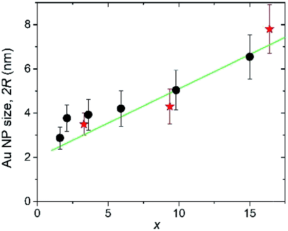 | ||
| Fig. 7 Dependence of the Au NP size (2R, here R is the spherical NP radius) on the Au concentration (x) in the AuxC60 mixture films as obtained from the TEM analysis (red stars) and from the Scherrer analysis of the XRD line-broadening (black circles). | ||
The 2R(x) dependence (here, L = 2R) obtained from XRD using eqn (1) (filled circles in Fig. 7) correlates nicely with the results obtained from TEM (filled stars). This correlation between the XRD and TEM results nicely confirms the single-crystalline origin of the Au NPs. The XRD analysis of the Au (111) peak width allowed us to specify the R(x) dependence as R(x) = (1.12 + 0.155 × x) nm (straight green line in Fig. 7). Together with the equation describing the concentration-dependence of the distance ΔL between the nearest Au NPs in the AuxC60 nanocomposite ΔL(x) = R(x)[4π/3(1 + β/x)]1/3,22 the evaluated equation R(x) allows one to predict the material nanostructure and the properties related to the NP-subsystem (for instance, plasmonic properties22).
From the interplanar spacings d111 of fcc-Au and fcc-C60, which were calculated from the positions of the respective diffraction lines 111 using the Bragg equation, the lattice deformations Δd/d0 = (d111 − d111,0)/d111,0 were determined. For C60, we used d111,0 = 8.28 Å, which corresponds to the undoped fcc-C60 film. For fcc-Au, the reference lattice spacing was taken as d111,0 = 2.35 Å,38 which corresponds to the lattice spacing in the bulk fcc-Au crystal. The concentration-dependence of the lattice deformations in Au NPs and the C60 nanocrystals is depicted in Fig. 8. Using the correlation between the Au NP size 2R (Fig. 7) and the relative change in the interplanar spacing 111 found for the Au NP-crystals at the respective x (Fig. 8), we confirmed that the Au lattice contracted with decreasing NP size in very small Au NPs (2R < 8 nm), which should yield a consequent increase in electron density.39 This remarkable result has fundamental importance and demonstrates the NP size threshold launching the quantum size effects in the smaller Au NPs and yielding intriguing quantum phenomena such as quantum plasmons.22,39–41
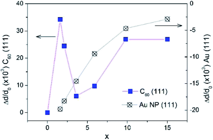 | ||
| Fig. 8 The relative change of lattice parameter in fcc-C60 (blue boxes) and in fcc-Au NPs (crossed circles) upon increase of Au concentration x in the AuxC60 mixture films. | ||
In contrast to the monotonous lattice contraction observed for fcc-Au NPs in AuxC60 nanocomposites with increasing Au content, the crystal structure of fcc-C60 experiences a non-monotonous expansion, which reaches its maximum for the Au concentration of about x = 1.6 in the XRD-studied AuxC60 samples (Fig. 8). The maximum lattice expansion in the mixture films with a small amount of Au can be explained by the intercalation of Au atoms into the pores of the fcc-C60 lattice.15 The comparison of the Au atomic radius (Ra = 1.36 Å (ref. 38)) with the radii of the interstitial fcc-C60 lattice pores (1.12 Å for the tetrahedral pores and 2.07 Å for the octahedral pores42) argues that the observed lattice expansion is caused by the intercalation of single Au atoms into the tetrahedral (TH) pores. Evidently, the intercalation of the Au atoms into the octahedral (OH) pores should not expand the fcc-C60 lattice. This argument implies that Au occupation of the TH pores is an important mechanism of the structure assembly in the R1 interval. The rapid relaxation of the C60 lattice distortion at higher x (i.e., x > 1.6) can be related to the growth and agglomeration of the Au NPs in the C60-matrix (see previous sections).
Indeed, as seen from Fig. 8, great relaxation of the C60 lattice expansion occurs at higher x, in particular when x exceeds the critical point xc1. This relaxation effect reflects the crucial change in the structure assembly mechanism when the mixture film belongs to the R2 interval. It is clear that the TH-pore intercalation by Au in the mixture films with x > 1 will greatly increase the C60 lattice distortion due to the filling of the TH pores situated in the vicinity of the already Au-filled ones (there are only two TH pores per C60 molecule in the fcc-C60 (ref. 42)). At this stage of the TH-pore intercalations, the increasing fcc-C60 distortion should be followed by the processes releasing the C60 lattice distortions, for instance, through redistribution of the Au atoms between the small TH- and large OH-pores. The latter processes will initiate the abundant filling of the OH-pores and, respectively, should yield Au clustering.15
The increase in the C60 lattice distortion at higher x within the R2 interval (roughly at x > 7, see Fig. 8) is probably caused by complex effects of Au intercalation and nucleation/growth of Au clusters.
C5 Raman spectra: Au and C60 coupling in the mixture films
Fig. 9 depicts the Raman spectra of the AuxC60 films. The Raman spectrum of the undoped C60 film (x = 0) is also shown in the plot for comparison.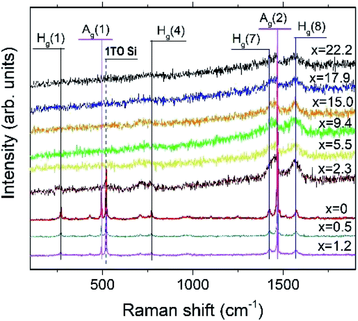 | ||
| Fig. 9 Raman spectra of the AuxC60 films with different Au concentrations (x). The x values are shown for the respective spectra. Some of the C60 vibration modes with Ag and Hg symmetry are indicated by vertical lines. The position of the intense 1TO Si(100) mode is indicated by the dashed vertical line (see text). | ||
The Raman spectrum of the undoped C60 film reveals ten well-resolved C60 Raman modes (two of Ag symmetry and eight of Hg symmetry, some of the modes are indicated by vertical lines in Fig. 9), the positions of which agree very well with those reported in the literature.42 In particular, the pure tangential Ag(2) vibration mode (the strongest Raman mode of C60) and the pure radial Ag(1) vibration mode appear at the wavenumbers of 1469 cm−1 and 495 cm−1, respectively. In addition to the C60 Raman modes, two vibration modes from the Si(100) substrate (the strong 1TO mode at 520 cm−1 and the weak and broad 2TO mode at around 950 cm−143) were also observed.
The spectra of the mixture films with low Au concentration (up to about x = 1.2, R1 interval) demonstrate the reduction of the intensity of the C60 vibration modes (see the spectra at the bottom of the graph in Fig. 9). Such a variation in the vibration spectra and the absence of any shift in the Ag(2) peak imply rather weak (van der Waals-like) interactions between Au and C60 in the dilute mixture films (the absence of the peak shift reflects the absence of Au–C60 charge transfer in the mixture42,44). However, if the Au concentration increases up to about x = 2.3 or higher (R2 interval), the spectra show dramatic reduction and broadening of the vibration modes (see the spectra in the upper part of the graph in Fig. 9). These features of the Raman spectra recorded from the AuxC60 films with the enhanced x (corresponding to the R2 interval) indicate strong electron–phonon coupling associated with efficient Au–C60 electronic interactions in the mixture films.42,45 The electron–phonon coupling caused the merging of the Hg(7) and Ag(2) peaks and growth of the Hg(8) peak (cf.Fig. 9). Other vibration modes in the Raman spectra of mixture films with x > 1.2 were poorly distinguished.
In order to quantify the Au–C60 electronic interactions in the mixture films, we performed a Lorentz analysis of the Raman spectra in the wavenumber range including the Hg(7) and Ag(2) modes.46Fig. 10 demonstrates some details of the Raman spectral analysis carried out for the selected mixture films, which belong to the R2 and R3 intervals.
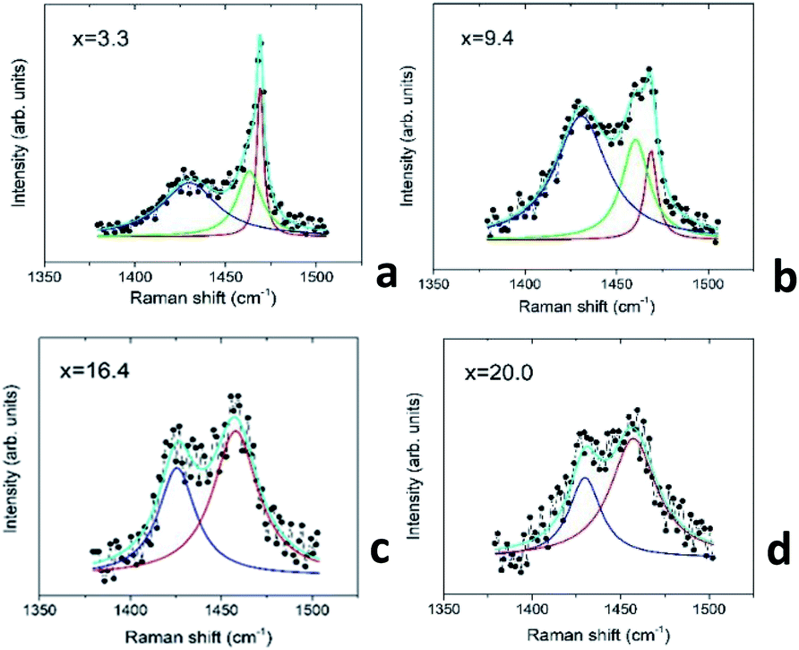 | ||
| Fig. 10 Raman spectra of the AuxC60 mixture films near the positions of the Hg(7) and Ag(2) modes of C60: (a and b) the mixture films from the interval R2; (c and d) the mixture films from the interval R3. The experimental spectra (black dots) fitted by a superposition of Lorentzians (light-blue line). See description in the text. | ||
The performed Lorentz analysis argues that the Raman spectra of the films from the R2 interval (see Fig. 10a and b) consist of two peaks in the vicinity of the Ag(2) mode, namely the non-shifted Ag(2) C60 peak centred at 1469 cm−1 and the similar peak shifted by about 6–8 cm−1 to the lower wavenumbers with respect to that in the pristine C60 (downshifted Ag(2) mode). The increase in x in the AuxC60 film resulted in a decrease in the intensity of the non-shifted peak and the increase in the intensity of the downshifted one (see Fig. 10a and b). The Raman spectra of the AuxC60 films belonging to the R3 interval show only one Ag(2) peak downshifted by about 10 cm−1 (Fig. 10c and d).
The observed features of the Raman spectra indicated a crucial change in the Au–C60 electronic interaction caused by variation in the Au concentration x in the AuxC60 mixture films. The Raman spectra confirmed the survival of the C60 molecules in the mixture films, as was already established by XRD (see the previous section).
D. Discussion
The AFM analysis of the AuxC60 mixture films enabled the selection of three composition intervals, i.e., x < 1.7 (R1), 1.7 < x < 16.4 (R2) and x > 16.4 (R3), with different mechanisms of structural self-assembly (see Fig. 2). The structure assembly in the rough films from the interval R1 proceeded mainly through the Au intercalation into the TH pores of the fcc-C60 lattice. The R2 (smooth films) and R3 (medium rough films) intervals identified the AuxC60 films in which the structure assembly was dominated by the Au clustering.In order to designate the border between the R1 and R2 intervals, we introduced the critical point xc1 whose value was estimated by AFM as xc1 ≈ 1.7 (see Fig. 2b). This value of xc1 is satisfactorily supported by the optical spectra.22
According to the Raman spectra and the XRD study of the films with x < xc1 (see Fig. 8), the TH-intercalated Au atoms dominating in the structure of the films from this x interval do not couple strongly with the surrounding C60 molecules because no Au–C60 charge transfer occurs (see the previous section). This means that the intercalated Au atoms do not lose any electrons and, therefore, the radius of the Au atoms has a maximum value (i.e., Ra = 1.36 Å). Evidently, the intercalation of such Au atoms into the relatively small TH pores (with a radius of 1.12 Å) caused a strong distortion of the fcc-C60 lattice, which was detected by XRD (see Fig. 7b). It was expected that the lattice distortion accumulating during the Au intercalation of the TH pores could cause a shift in the C60 molecules from the lattice nodes to the interstitial positions. Indeed, the formation of the irregular hillocks on the surface of the films from interval R1 detected by AFM could be related to the C60 interstitials collected on the film surface (see Fig. 2).
The increase in x in the interval of 1 < x < xc1 (interval R1) will strongly increase the C60 lattice distortion (see Fig. 8). This will induce the TH-to-OH Au redistribution and launch the nucleation of Au clusters in the OH-pores if the Au concentration reaches xc1.15 The TH-to-OH Au redistribution can occur in parallel with the formation of the C60 vacancies that arise together with the C60 interstitials (see above), which also belong to the effective sources of Au clustering.
In the R2 interval, the increase in the Au concentration in the AuxC60 mixture causes an abundant increase in the number of Au clusters and also some increase in the cluster size (see the TEM results in Fig. 3). The latter effect is promoted by phase separation, which yields the coexistence of two C60-based phases in the mixture film. Indeed, the Raman spectra of the relevant films (see Fig. 10a and b) include two main vibration modes, namely the main mode at 1469 cm−1 (a non-shifted mode, corresponding to the non-bonding C60 molecules) and the one downshifted by 6–8 cm−1 corresponding to the C60 molecules charged by about one extra electron (the Raman shift-to-charge conversion coefficient is −6.1 cm−1 per e, where e is the electron charge42,44). The Raman spectral analysis allowed us to conclude that the charged C60 molecules are coupled with the Au clusters. Similar charging effects were reported for C60 deposited on the surface of the Au film.47 The non-shifted Ag(2) mode could be related to the non-bonding C60 or Au-intercalated C60 phase (see the previous section).
In the R3 interval, the Au NP size rapidly increased with x through the coalescence of the small clusters (see the TEM-related section). The Raman spectra of such films show only one Ag(2) mode downshifted by about 10 cm−1, which reflects the C60 charging by about −1.6e (see Fig. 10c and d). This means that all C60 molecules surviving in the mixture film are coupled with the Au NP surface. The enhanced C60 charging affirms that most C60 molecules existing in such films are coupled with two Au NPs. In other words, Au NPs in the films from the R3 interval are touching or separated by one layer of the C60 molecules.
E. Conclusions
The systematic study of the nanostructures in vapour-deposited AuxC60 mixture films with the Au concentrations of 0 < x < 30 has revealed important regularities in the structure assembly. The application of several highly efficient techniques has allowed us to distinguish three intervals of x, enabling the specific mechanisms of the structure assembly in the mixture films. In the low-x interval, R1 (0 < x < xc1; xc1 ≈ 1.7), the Au atoms are intercalated into the tetrahedral pores of the C60 lattice. The second interval of x (R2, xc1 < x < xc2, xc2 ≈ 16.4) is designated by composite nanostructures formed through the pronounced Au clustering in the mixture films. The size of the Au clusters was found to gradually increase with x, and the Au NP radius R can be roughly approximated as R(x) = (1.12 + 0.155 × x) nm. The nanostructure of the AuxC60 films from the third interval of x (R3, x > xc2) was determined mainly by coalescence of the enlarged Au NPs, which was partially inhibited by monolayers of C60 separating the neighbouring Au NPs.Taking into account the plasmonic properties of AuxC60 reported recently, the most attractive compositions should be expected in the concentration interval of 1.7 < x < 16.4. In particular, we showed that this interval of x produces AuxC60 nanocomposites, in which the quantum-size effects could be essential and will be more efficient at lower x approaching xc1. The established regularities in the structure assembly allow one to consider the AuxC60 nanocomposites as a precursor of quantum materials with encouraging application potential in advanced technologies related to, for instance, nano-electronics and nano-plasmonics.
Conflicts of interest
There are no conflicts to declare.Acknowledgements
This work was partially supported by GACR (grant 19-02804S). The RBS measurements were implemented using the CANAM infrastructure supported through MEYS (the project No. LM2011019).References
- M. Scheele, W. Brütting and F. Schreiber, Phys. Chem. Chem. Phys., 2015, 17, 97–111 RSC.
- E. Goiri, P. Borghetti, A. El-Sayed, J. E. Ortega and D. G. de Oteyza, Adv. Mater., 2016, 28, 1340–1368 CrossRef PubMed.
- Y. Cui, B. Li, H. He, W. Zhou, B. Chen and G. Qian, Acc. Chem. Res., 2016, 49, 483–493 CrossRef PubMed.
- J. D. Sosa, T. F. Bennett, K. J. Nelms, B. M. Liu, R. C. Tovar and Y. Liu, Crystals, 2018, 8, 325 CrossRef.
- M. Cinchetti, V. A. Dediu and L. E. Hueso, Nat. Mater., 2017, 16, 507–515 CrossRef PubMed.
- R. Otero, A. L. Vázquez de Parga and J. M. Gallego, Surf. Sci. Rep., 2017, 72, 105–145 CrossRef.
- K. V. Raman, A. M. Kamerbeek, A. Mukherjee, N. Atodiresei, T. K. Sen, P. Lazić, V. Caciuc, R. Michel, D. Stalke, S. K. Mandal, S. Blűgel, M. Műnzenberg and J. S. Moodera, Nature, 2013, 493, 509–513 CrossRef PubMed.
- M. Gobbi, F. Golmar, R. Llopis, F. Casanova and L. E. Hueso, Adv. Mater., 2011, 23, 1609–1613 CrossRef.
- F. Al Ma'Mari, T. Moorsom, G. Teobaldi, W. Deacon, T. Prokscha, H. Luetkens, S. Lee, G. E. Sterbinsky, D. A. Arena, D. A. MacLaren, M. Flokstra, M. Ali, M. C. Wheeler, G. Burnell, B. J. Hickey and O. Cespedes, Nature, 2015, 524, 69–74 CrossRef.
- X. Li, Y. J. Tang, H. W. Zhao, W. Zhan, H. Wang and J. G. Hou, Appl. Phys. Lett., 2000, 77, 984–986 CrossRef.
- V. Lavrentiev, H. Abe, S. Yamamoto, H. Naramoto and K. Narumi, Mater. Lett., 2003, 57, 4093–4097 CrossRef.
- A. V. Talyzin and U. Jansson, Thin Solid Films, 2003, 429, 96–101 CrossRef.
- G. Yoshikawa, Y. Tsuruma, S. Ikeda and K. Saiki, Adv. Mater., 2010, 22, 43–46 CrossRef.
- R. Manaila, A. Belu-Marian, D. Macovei, C. Brehm, D. T. Marian and I. Baltog, J. Raman Spectrosc., 1999, 30, 1019–1025 CrossRef.
- V. Lavrentiev, A. Stupakov, M. Barchuk, I. Lavrentieva, J. Pokorný, J. Vacik, P. Čapková and A. Dejneka, Carbon, 2016, 103, 425–435 CrossRef.
- R. C. Haddon, Acc. Chem. Res., 1992, 25, 127–133 CrossRef.
- J. Nishinaga, T. Aihara, H. Yamagata and Y. Horikoshi, J. Cryst. Growth, 2005, 278, 633–637 CrossRef.
- J. Vacik, V. Lavrentiev, K. Novotna, L. Bacakova, V. Lisa, V. Vorlicek and R. Fajgar, Diamond Relat. Mater., 2010, 19, 242–246 CrossRef.
- H. Zare-Kolsaraki and H. Micklitz, Eur. Phys. J. B, 2004, 40, 103–109 CrossRef.
- S. Sakai, K. Yakushiji, S. Mitani, K. Takanashi, H. Naramoto, P. V. Avramov, K. Narumi, V. Lavrentiev and Y. Maeda, Appl. Phys. Lett., 2006, 89, 113118 CrossRef.
- S. Miwa, M. Shiraishi, S. Tanabe, M. Mizuguchi, T. Shinjo and Y. Suzuki, Phys. Rev. B: Condens. Matter Mater. Phys., 2007, 76, 214414 CrossRef.
- V. Lavrentiev, D. Chvostova, M. Motylenko, J. Vacik, D. Rafaja and A. Dejneka, Nanotechnology, 2019, 30, 365001 CrossRef.
- A. Devenyi, R. Manaila, A. Belu-Marian, D. Macovei, M. Manciu, E. M. Popescu, M. Tanase, D. Fratiloiu, N. D. Mihai, P. B. Barna, J. Labar, G. Safran, A. Kovacs and T. Braun, Thin Solid Films, 1998, 335, 258–265 CrossRef; R. Singhal, P. Sharma, R. Vishno and D. K. Avasthi, J. Alloys Compd., 2017, 696, 9–15 CrossRef.
- M. Mayer, Nucl. Instr. and Meth. B, 2014, 332, 176–180 CrossRef.
- G. Götz and K. Gärtner, High-Energy Ion Beam Analysis of Solids, Physical Research, vol. 6, Akademie, Berlin, 1988 Search PubMed.
- J. L. Lábár, Microsc. Microanal., 2008, 14, 287–295 CrossRef.
- J. L. Lábár, Ultramicroscopy, 2005, 103, 237–249 CrossRef.
- H.-G. Liao, Y. Shao, C. Wang, Y. Lin, Y.-X. Jiang and S.-G. Sun, Mater. Lett., 2014, 116, 299–303 CrossRef CAS.
- Y. Q. Wang, W. S. Liang and C. Y. Geng, Nanoscale Res. Lett., 2009, 4, 684–688 CrossRef CAS.
- A. Ulvestad, J. N. Clark, R. Harder, I. K. Robinson and O. G. Shpyrko, Nano Lett., 2015, 15, 4066–4070 CrossRef CAS.
- M. Song, G. Zhou, N. Lu, E. Nakouzi, H. Wang and D. Li, Science, 2020, 367, 40–45 CrossRef CAS.
- M. Valášková, G. S. Martynková, J. Lešková, P. Čapková, V. Klemm and D. Rafaja, J. Nanosci. Nanotechnol., 2008, 8, 3050–3058 CrossRef.
- C. Elschner, A. A. Levin, L. Wilde, J. Grenzer, C. Schroer, K. Leo and M. Riede, J. Appl. Crystallogr., 2011, 44, 983–990 CrossRef CAS.
- T. Itoh, S. Nitta and S. Nonomura, Appl. Surf. Sci., 1997, 113/114, 282–285 CrossRef CAS.
- M. Dopita, M. Emmel, A. Salomon, M. Rudolph, Z. Matěj, C. G. Aneziris and D. Rafaja, Carbon, 2015, 81, 272–283 CrossRef CAS.
- M. M. Hall, V. G. Veeraraghavan, H. Rubin and P. G. Winchell, J. Appl. Crystallogr., 1977, 10, 66–68 CrossRef.
- A. L. A. Patterson, Phys. Rev., 1939, 56, 978–982 CrossRef CAS.
- C. Kittel, Introduction to Solid State Physics, Wiley, New York, 7th edn, 1996 Search PubMed.
- V. Amendola, R. Pilot, M. Frasconi, O. M. Maragò and M. A. Iatì, J. Phys.: Condens. Matter, 2017, 29, 203002 CrossRef.
- H.-C. Weissker, H. Barron Escobar, V. D. Thanthirige, K. Kwak, D. Lee, G. Ramakrishna, R. L. Whetten and X. López-Lozano, Nat. Commun., 2014, 5, 3785 CrossRef.
- J. A. Scholl, A. L. Koh and J. A. Dionne, Nature, 2012, 483, 421–428 CrossRef CAS PubMed.
- M. S. Dresselhaus, G. Dresselhaus and P. C. Eklund, Science of Fullerenes and Carbon Nanotubes, Academic Press, San Diego, 1996 Search PubMed.
- V. Lavrentiev, J. Vacik, V. Vorlicek and V. Vosecek, Phys. Status Solidi B, 2010, 247, 2022–2026 CrossRef CAS.
- T. Pichler, M. Matus, J. Kürti and H. Kuzmany, Phys. Rev. B: Condens. Matter Mater. Phys., 1992, 45, 13841–13844 CrossRef CAS PubMed.
- M. Yao, V. Pischedda and A. S. Miguel, J. Phys.: Condens. Matter, 2011, 23, 115701 CrossRef.
- A. C. Ferrari and J. Robertson, Phys. Rev. B: Condens. Matter Mater. Phys., 2000, 61, 14095 CrossRef CAS.
- M. R. C. Hunt, S. Modesti, P. Rudolf and R. E. Palmer, Phys. Rev. B: Condens. Matter Mater. Phys., 1995, 51, 10039–10047 CrossRef CAS.
| This journal is © The Royal Society of Chemistry 2020 |