
 Open Access Article
 This Open Access Article is licensed under a Creative Commons Attribution-Non Commercial 3.0 Unported Licence
A high-performance and flexible thermoelectric generator based on the solution-processed composites of reduced graphene oxide nanosheets and bismuth telluride nanoplates†
Defang
Ding‡
a,
Fengming
Sun‡
a,
Fan
Xia
 *a and
Zhiyong
Tang
bc
*a and
Zhiyong
Tang
bc
aEngineering Research Center of Nano-Geomaterials of Ministry of Education, Faculty of Materials Science and Chemistry, China University of Geosciences (CUG), 388 Lumo Road, Wuhan 430074, P. R. China. E-mail: xiafan@cug.edu.cn; xiafan@hust.edu.cn
bCAS Key Laboratory of Nanosystem and Hierarchical Fabrication, CAS Center for Excellence in Nanoscience, National Center for Nanoscience and Technology, No. 11, Beiyitiao, Zhongguancun, Beijing, 100190, P. R. China
cUniversity of Chinese Academy of Sciences, 19A Yuquan Rd, Shijingshan District, Beijing, 100049 P. R. China
First published on 12th June 2020
Abstract
The fabrication of a flexible thermoelectric generator (TEG) with both high power output and good flexibility has drawn considerable attention. Solution-processed inorganic nanocrystals have good processibility in interface to retain excellent electrical properties of nanocrystals and can be processed into thin films on a flexible substrate by an easy scale-up printing or coating method. However, a high-performance TEG device based on inorganic solution-processed materials also poses challenges when it comes to flexibility of the whole device. Herein, flexible planar TEG devices are fabricated by printing an ink mixture comprising solution-processed bismuth telluride (Bi2Te3) nanoplates with reduced-graphene oxide (rGO) nanosheets onto flexible polyimide substrates. The interface treatment by hot ethylenediamine and the appropriate amount of rGO contribute to the high electrical properties of the material. Also, when rGO nanosheets of 1% mass ratio are added, the optimum power output of the corresponding rGO/Bi2Te3 TEG device with six elements reaches ∼1.72 μW at a temperature difference of 20 K. Moreover, owing to the contribution from flexible rGO nanosheets, the suitable thickness of each element, and the artful connection of elements with a soft copper wire in the devices, the 1% rGO/Bi2Te3 TEG device was found to be robust, and its electrical resistance merely changes by 2% after bending 1000 cycles on 5 mm in bending. These inorganic-based TEGs with both high performance and good flexibility will promote the development of new generation energy devices in the field of flexible electronics.
Introduction
Along with the rapid development of flexible electronics, particular attention has been paid to the flexible thin-film-based thermoelectric generator (TEG) devices because of their intriguing self-powering merit with no need of additional power managing components.1–4 An emerging method has been developed based on the solution-processed nanostructures,5–8 which are easily processed into thin films on the flexible substrates by low-temperature, low-cost, convenient and efficient means such as coating or printing.9–12 Moreover, bulk binary chalcogenides such as bismuth telluride (Bi2Te3), antimony telluride (Sb2Te3), and their alloys, which are the preferred choice for most flexible thermoelectric applications due to their excellent thermoelectric materials near room temperature,13–16 are usually difficult to be integrated into flexible devices because of the poor processability.17–19 In this case, the coating or printing method based-on solution-processed Bi2Te3 or Sb2Te3 nanocrystals should also be adopted. Also, it has been widely reported that these solution-processed films could retain the excellent electrical properties in high-performance electronic and optoelectronic devices on flexible substrates.20–23 Solution-processed inorganic nanocrystals have good processibility in the interface to retain the excellent electrical properties of the nanocrystals. In our previous study about the interface engineering in solution-processed nanocrystal thermoelectric thin films, we also demonstrated that the hot ethylenediamine can effectively strip the insulating organic ligands from the surface of the nanocrystals that hinder the charge transfer.24 Moreover, it is a facile and mild wet-chemical method. Therefore, coating or printing based-on Bi2Te3 or Sb2Te3 solution-processed nanocrystals is a compatible method to prepare flexible thin-film-based TEG devices.The power output of TEG devices depends on multiple parameters including the Seebeck coefficient (S) of materials, electrical conductivity (σ) of materials, thermal conductivity (κ) of materials, number of thermal elements (m), the temperature difference across the device (ΔT), and internal resistance of the device (Ri). In order to achieve a considerable power output, the thermoelectric properties of the materials including S, σ and κ must be mutually coordinated since high figure-of-merit (ZT = S2σT/κ,25–27T is the absolute temperature) of material is crucial for power output.1–4 In addition, Ri of TEG devices must be low. However, low Ri and good flexibility are usually difficult to be simultaneously achieved in one flexible TEG device. First, for example, organic semiconductors are suggested to be used in flexible thin-film-based TEG devices due to their intrinsic flexibility,28 but they encounter several limitations, e.g. rather low electrical conductivity and high contact resistance with the metal electrodes, leading to high Ri.29 On the contrary, the inorganic thermoelectric materials are able to resolve those problems and ultimately higher power output is expected, but the inorganic-based materials are usually rigid.29,30 Second, the rational design on the geometry of the thermal element is a prerequisite for decreasing Ri of the TEG device. For example, thermal elements should be characteristic of short length and large cross-section area for low Ri, but it is difficult to maintain ΔT when the length of the elements is extremely short. A large cross-section area demands high thickness and width of the element. However, increasing the width of the element would decrease the number of elements per unit area, giving rise to reduced power output. Also, extremely increasing the thickness of the element would increase the cracking risk during bending, leading to poor flexibility. Thereby, there must be a trade-off between the geometry of thermal elements and power output.31 In addition to thermal elements, the flexibility of a TEG device also is subjected to its connection of thermal elements, particularly the materials of connection, which are actually crucial for the whole device.32,33 Even if the thermal elements possess good flexibility, the whole TEG device with rigid connection materials could not tolerate cycle bending. However, not enough attention is paid to this issue. Altogether, in order to acquire flexible thin-film based TEG devices with high performance, a systematic design principle needs to be established, which includes a judicious selection of active materials, precise structural control on the thermal elements, appropriate design of connection manner, and convenient and efficient preparation of thin films.
Herein, we demonstrate the facile fabrication of the flexible planar TEG devices containing six elements by printing the solution-processed two-dimensional (2D) Bi2Te3 nanoplates with reduced-graphene oxide (rGO) nanosheets in different mass ratio onto the polyimide substrates with shadow masks (Scheme 1). The hot ethylenediamine was employed to remove the organic ligands of Bi2Te3 nanoplates,24,34 where the GOs transformed into rGOs due to the reduction from hot ethylenediamine.34 Also, the thermal elements are connected by the soft copper wires with silver paste in these six-element devices. Impressively, the 1% rGO/Bi2Te3 thin film achieves the ZT of 0.4 at 400 K. The optimum power output (Pmax) of the 1% rGO/Bi2Te3 TEG devices, with six elements of the size of 10 mm × 3 mm × 40 μm, reaches ∼1.72 μW at ΔT = 20 K and ∼15.22 μW at ΔT = 60 K. More importantly, this 1% rGO/Bi2Te3 TEG device is robust upon repeated flexing to bending radius of down to 5 mm, highlighting the application potential of the solution-processed nanomaterials in flexible electronics.
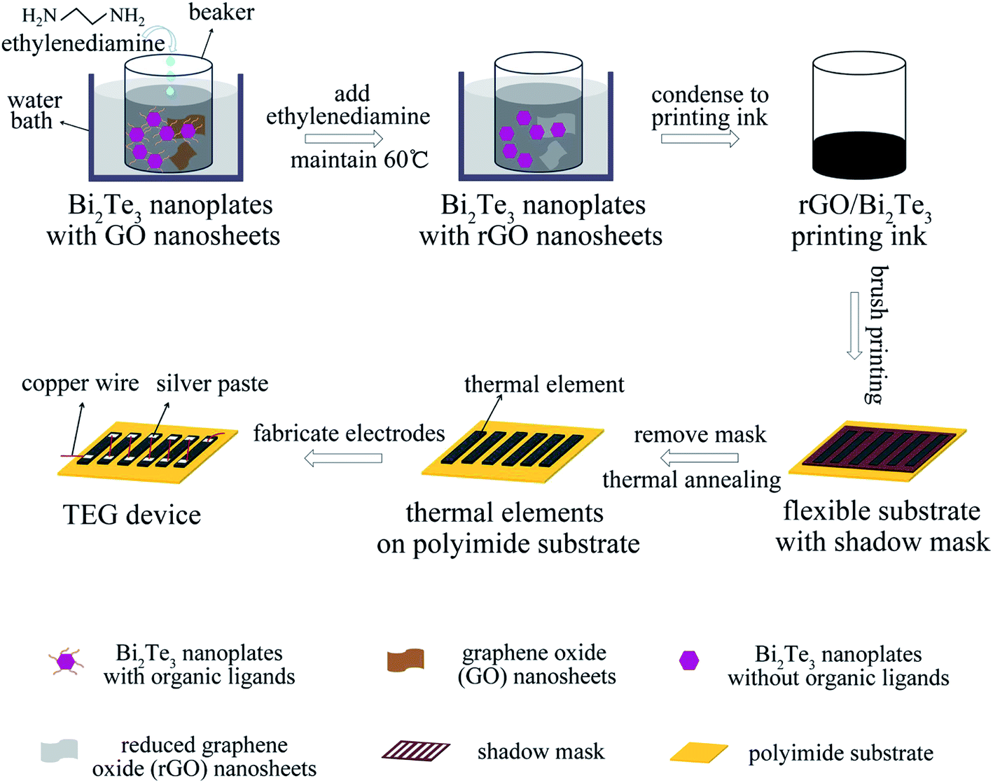 | ||
| Scheme 1 Schematic of the fabrication of flexible six-element planar TEG devices by printing. Bi2Te3 nanoplates with GO nanosheets were treated by hot ethylenediamine to remove the organic ligands of Bi2Te3, and the GO transformed to rGO with the hot ethylenediamine. Subsequently, rGO/Bi2Te3 was slowly condensed to inks for printing on polyimide substrates with the shadow mask. After removing the shadow mask and thermal annealing process, the copper wires connected to the thermal elements by silver paste were used as electrodes in the six-element devices. | ||
Experimental
Materials
Sodium tellurite (NaTeO3, >99.99%), bismuth nitrate pentahydrate (Bi(NO3)3·5H2O, >90%), sodium hydroxide (NaOH, >90%), poly(vinyl pyrrolidone) (PVP, MW ≈ 40![[thin space (1/6-em)]](https://www.rsc.org/images/entities/char_2009.gif) 000) and ethylene glycol (EG) were all purchased from Alfa Aesar. Ethylenediamine (C2H8N2) (99%) was obtained from Acros. Graphite powder (325 mesh), potassium permanganate (KMnO4, >90%), concentrated sulfuric acid (H2SO4, 98%), hydrogen peroxide (H2O2, 30%), hydrochloric acid (HCl, 37%), anhydrous acetone and isopropanol were supplied by Sinopharm. All the chemicals were used as received without further purification.
000) and ethylene glycol (EG) were all purchased from Alfa Aesar. Ethylenediamine (C2H8N2) (99%) was obtained from Acros. Graphite powder (325 mesh), potassium permanganate (KMnO4, >90%), concentrated sulfuric acid (H2SO4, 98%), hydrogen peroxide (H2O2, 30%), hydrochloric acid (HCl, 37%), anhydrous acetone and isopropanol were supplied by Sinopharm. All the chemicals were used as received without further purification.
Synthesis of bismuth telluride (Bi2Te3) nanoplates
Bi2Te3 nanoplates were synthesized according to the literature.19 Typically, 0.194 g Bi(NO3)3·5H2O (0.4 mmol), 0.133 g NaTeO3 (0.6 mmol), 0.32 g NaOH (8 mmol) and 0.4446 g PVP (4 mmol) were dissolved in 20 mL ethylene glycol in a 50 mL three-neck flask equipped with a thermocouple and reflux condenser. The mixture was stirred and heated to 60 °C on a heating mantle until the solution became transparent. Then the temperature was raised to 190 °C in 30 min, and the solution immediately turned black. After holding the temperature for 3 h, the heating mantle was removed and the mixture was allowed to cool down to room temperature naturally. The mixture was separated into two 50 mL centrifuge tubes, and 20 mL isopropanol and 10 mL acetone were added into both of the tubes, and then centrifuged them at 10000 rpm for 8 min. The supernatant was discarded, while the solid was dispersed in fresh 40 mL isopropanol and then centrifuged them at 8000 rpm for 5 min. The washing steps were repeated with isopropanol for two more times. The final products were collected and dispersed in isopropanol for further use.
Synthesis of the composites of graphene oxide (GO) nanosheets and Bi2Te3 nanoplates
GO was synthesized by the Hummers' method.35 The as-synthesized GO was freeze-dried for further use. A certain mass ratio of GO power was ultrasonically dispersed in ethylene glycol for 1 h. And then, the solution of GO in ethylene glycol was used as a precursor being added into the above synthesis process of Bi2Te3 nanoplates. For example, 1% mass ratio of dried GO (∼2.5 mg), 0.194 g Bi(NO3)3·5H2O (0.4 mmol), 0.133 g NaTeO3 (0.6 mmol), 0.32 g NaOH (8 mmol) and 0.4446 g PVP (4 mmol) were dissolved in 20 mL ethylene glycol, and the following synthesis steps were similar to the above process.Organic surfactant removing
Before printing or coating on the substrate, PVP polymer on Bi2Te3 nanoplate surfaces (or in GO/Bi2Te3 composites), which would hinder the charge carrier transport, was stripped. Typically, ∼0.4 mmol nanoplates were dispersed in 15 mL solution of ethylenediamine in isopropanol (1 M), and then the mixture was stirred at 60 °C for 12 h. After that, the products were centrifuged at 8000 rpm for 5 min. The supernatant was discarded, while the solid was dispersed in fresh 40 mL isopropanol, the washing steps were repeated with isopropanol for two more times. The final products were dispersed in isopropanol. Here it needs to be pointed out that GO turned to reduced-GO (rGO) during the treatment with hot ethylenediamine, as shown in Raman spectroscopy results (Fig. S3†). Therefore, the composites were mixtures of rGO nanosheets and Bi2Te3 nanoplates.Fabrication of flexible six-element planar TEG device and testing
To print the solution on the polyimide substrate to obtain flexible planar TEG devices, the solution of Bi2Te3 nanoplates or rGO/Bi2Te3 composites after the PVP removal was slowly condensed to ink in a vacuum (∼4 mmol nanoplates in 1 mL isopropanol). Subsequently, the ink was treated in an ultrasonic bath to keep the high dispersion of nanoplates. Then, the TE inks were printed on polyimide substrates with a shadow mask to form six 10 mm × 3 mm × 40 μm thermal elements using write printing, followed by annealing at 380 °C for 1 h to form solid thick films. Each thermal element was connected in series with a copper wire (50 μm in diameter) using conductive silver paste, as shown in Scheme S1.† In order to reduce the contact resistance, the TEG devices with silver paste were cured at 60 °C for 4 h in a vacuum oven.Two thermocouples of 50 μm in diameter were pasted on the hot and cold sides of the device to measure the temperature difference. The temperature difference across the TEG devices was created by heating the hot-side while maintaining the cold-side temperature, held by a temperature controller.
Results and discussion
Morphology and structure characterization of the rGO/Bi2Te3 composite films
The morphologies of the rGO/Bi2Te3 composite films, i.e. the thermal element, from the six-element planar TEG devices are discerned by SEM (Fig. 1). From the surface SEM images, it is clear that with the increasing percentage of rGO from 0 to 2%, the rGO nanosheets cover the Bi2Te3 nanoplates like “gossamer”, and the rGO is uniformly distributed in the Bi2Te3 nanoplate films. The thickness of all the films is controlled by about 40 μm. In theory, the thicker the films, the larger the cross-section area of the films, which can efficiently decrease the internal resistance of the device. However, the thickness of the films should coordinate with the flexibility of the device, after all, excessively thick films crack easily during bending. Hence, we controlled the films (elements) to a moderate thickness, ∼40 μm. The XRD patterns of the pure Bi2Te3 and 1% rGO/Bi2Te3 composites films before and after annealing are shown in Fig. 1i. The three XRD plots show similar patterns. The peaks can be indexed to PDF no. 08-0021 of Bi2Te3. Moreover, there is no characteristic peak of rGO in the pattern of 1% rGO/Bi2Te3 film. The rGO's peaks should be hindered by the strong peaks of Bi2Te3 due to the low weight percentage of rGO in the composite films. There is no obvious difference between 1% rGO/Bi2Te3 composites films before and after annealing.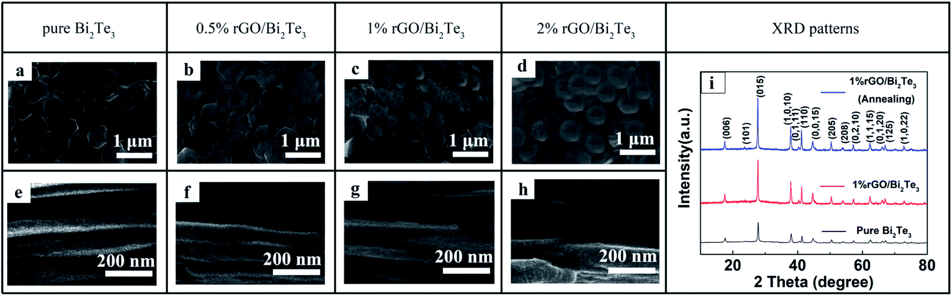 | ||
| Fig. 1 Surface and cross-sectional SEM images of Bi2Te3 nanoplate films with different mass ratio of rGO nanosheets: (a) and (e) pure Bi2Te3, (b) and (f) 0.5% rGO/Bi2Te3, (c) and (g) 1% rGO/Bi2Te3, and (d) and (h) 2% rGO/Bi2Te3; (i) XRD patterns of the pure Bi2Te3 and 1% rGO/Bi2Te3 composites films before and after annealing. | ||
Thermoelectric properties of the rGO/Bi2Te3 composite films
Fig. 2 summarizes the temperature-dependent thermoelectric properties of the films made from Bi2Te3 nanoplates or rGO/Bi2Te3 composites. It is seen that all the films possess negative S (Fig. 2a), manifesting that films are all n-type in nature. With the increasing percentage of rGO, the absolute value of S of the composite films is reduced, suggesting that the introduction of rGO is harmful to S of n-type Bi2Te3 nanoplate films. Since pure rGO is known to be p-type,36,37 and its positive S was experimentally confirmed by us, as shown in Fig. S5a.† Therefore, the addition of rGO would counteract the whole S of the composite films due to the opposite sign of S.38Fig. 2b displays that σ of rGO/Bi2Te3 composite films are significantly enhanced with the addition of rGO. The electron mobility (μ) is largely improved from 59.08 cm2 V−1 s−1 to 138.79 cm2 V−1 s−1 by adding rGO, whereas the change in tthe electron concentration (n) is small (Table 1). So, the improved μ should be responsible for the enhanced σ according to the approximate relationship σ = enμ,39 where e is the charge per carrier. rGO in the composite likely provides extra transfer channels for electrons,40,41 which results in the increased μ. Meanwhile, n changes little with the addition of rGO, which means that the n plays little role in the S. The S2σ of all the films are then calculated (Fig. 2c). Notably, the 1% rGO/Bi2Te3 composite films exhibit the best performance of 3.2 μW cm−1 K−2 at 300 K and 4.6 μW cm−1 K−2 at 400 K due to the balance between S and σ. The thermal conductivity (κ) of the rGO/Bi2Te3 composites is increased with the increase in the percentage of rGO (Fig. 2d). We also tested the κ of pure rGO films (Fig. S5d†). It is about 14.3 W m−1 K−1, which is much higher than that of the Bi2Te3 nanoplate film (∼0.42 W m−1 K−1). The rGO nanosheets will facilitate the heat conduction,42 thus increasing the κ of the rGO/Bi2Te3 composites. After the integration of S, σ and κ into the ZT value, the 1% rGO/Bi2Te3 composite films exhibit the best ZT of 0.2 at 300 K and 0.4 at 400 K as shown in Fig. 2e.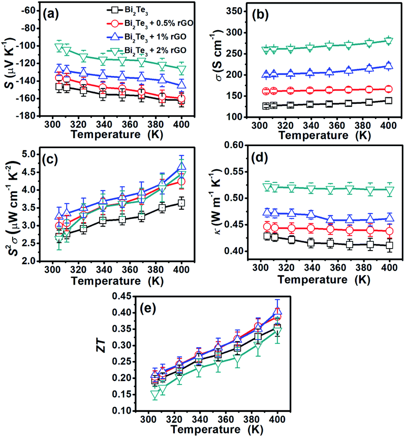 | ||
| Fig. 2 Temperature dependent (a) Seebeck coefficient (S), (b) electrical conductivity (σ), (c) power factor (S2σ), (d) thermal conductivity (κ) and (e) figure-of-merit (ZT) of Bi2Te3 nanoplate films with different mass ratio of rGO nanosheets. The legends in (a) are applied to all the figures. Error bars are estimated from repeatability of the experimental results: for each material-making condition, three samples are prepared and measured. With the increasing percentage of rGO, the S of the rGO/Bi2Te3 composite films is reduced but the σ and κ are increased. Finally, the 1% rGO/Bi2Te3 composite films exhibit the best ZT value calculated by the three factors (ZT = S2σT/κ). | ||
| Samples | n (1019 cm−3) | μ H (cm2 V−1 s−1) | σ (S cm−1) |
|---|---|---|---|
| Bi2Te3 | 1.33 | 59.08 | 125.7 |
| 0.5% rGO/Bi2Te3 | 1.26 | 79.79 | 160.8 |
| 1% rGO/Bi2Te3 | 1.21 | 103.27 | 199.9 |
| 2% rGO/Bi2Te3 | 1.17 | 138.79 | 259.8 |
| rGO film | 3.59 | 48.25 | 277.3 |
A transport mechanism in the rGO/Bi2Te3 composite films is proposed as follows. There are tremendous interfaces between rGO and Bi2Te3. Moroever, the energy barrier at the interfaces can filter the low-energy carriers and only high-energy carriers can pass through the barrier,43 which increases the whole S of samples. The energy filtering effect on the S also reduces the harmful effect from the p-type rGO, which, thus, maintains the S of rGO/Bi2Te3 film to relatively high n-type values. Simultaneously, the interface of Bi2Te3 nanoplates and the interface between rGO and Bi2Te3 can efficiently scatter phonons with relative wavelength.44 Therefore, we obtain low κ values for all the samples. Owing to the large number of interfaces between rGO, the κ of rGO/Bi2Te3 films are still at a relatively low value though the high κ of the added rGO.
The power output conclusion of all rGO/Bi2Te3 TEG devices
The thermoelectric output performances of the rGO/Bi2Te3 TEG devices are characterized. Fig. 3 summarizes the power output and operating voltage of TEG devices as a function of electrical current, which were tested by varying the external load resistance (Re). Note that Pmax is acquired when the external load resistance matches the internal resistance of the TEG devices. As indicated in Fig. 3a, with the increasing percentage of rGO from 0 to 0.5%, 1% and 2%, Pmax at ΔT = 20 K is 1.45 μW, 1.58 μW, 1.72 μW and 1.09 μW, respectively. Fig. 3b presents the corresponding operating voltage plots of four TEG devices. They are 7.98 mV, 7.95 mV, 7.32 mV and 5.85 mV, respectively (ΔT = 20 K) at their Pmax. Remarkably, the 1% rGO/Bi2Te3 TEG devices possess the highest Pmax.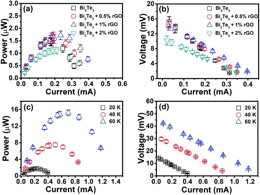 | ||
| Fig. 3 Output characterization: (a) and (b) power output and operating voltage of flexible TEG devices made from Bi2Te3 nanoplates with different mass ratio of rGO nanosheets at temperature difference of 20 K; (c) and (d) power output and operating voltage of 1% rGO/Bi2Te3 composite TEG devices at temperature difference of 20 K, 40 K and 60 K. Error bars are estimated from repeatability of the experimental results: for each condition, three samples are prepared and measured. The 1% rGO/Bi2Te3 TEG devices possess the highest Pmax. And larger ΔT brings higher power output and voltage. | ||
The Pmax of the TEG devices is defined by the equation Pmax = Voc2/(4Ri) when Ri = Re,9 where Voc (Voc = mSΔT) is the open circuit voltage of the TEG devices without the load and Ri is the internal resistance of the TEG devices. We also examined the Voc of TEG devices made from pure Bi2Te3 nanoplates as shown from the data in Fig. 4. Voc is approximately linear with ΔT. A video about the real-time measurements of Voc of the TEG is supplied in Video S1.† As displayed in the video, Voc of a TEG device is over 14 mV at ΔT = 20 K. Simultaneously, there is no significant change in the Voc in 24 hours as shown in Fig. S6,† which means a good stability for the TEG device.
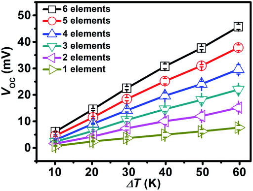 | ||
| Fig. 4 Open circuit voltage (ΔVoc) against temperature difference (ΔT) responsible for number of thermal elements of flexible TEG devices made from pure Bi2Te3 nanoplates. Error bars are estimated from repeatability of the experimental results: for each material-making condition, three samples are prepared and measured. | ||
To further explore the influence of ΔT on the power output and operating voltage, the TEG devices made from 1% rGO/Bi2Te3 nanoplate inks were investigated at ΔT of 20 K, 40 K and 60 K, as shown in Fig. 3c, with ΔT increasing, Pmax values are 1.72 μW, 7.48 μW and 15.22 μW, respectively, while the corresponding operating voltages at Pmax are 7.32 mV, 15.29 mV and 21.81 mV, respectively (Fig. 3d). Both results reveal that larger ΔT brings higher power output and voltage.
The flexibilities of rGO/Bi2Te3 TEG devices
Finally, the flexibilities of the pure Bi2Te3 and 1% rGO/Bi2Te3 TEG devices were inspected with a bending test. Fig. 5 presents the change rate of room-temperature electrical resistance (R/R0) with different bending radii and bending cycles, R0 and R are the resistances of devices before and after bending. The R of 1% rGO/Bi2Te3 device is almost unchanged when the bending radius was decreased from 6 mm to 4 mm as shown in Fig. 5a, and starts to significantly increase after the bending radius goes down to 2 mm. In contrast, the R of pure Bi2Te3 device starts to rapidly increase when the bending radius decreased from 4 mm to 2 mm. At the same time, as shown in Fig. 5b, the R of 1% rGO/Bi2Te3 device increases by 2% after 1000 bending cycles with 5 mm of bending radius, but the R of Bi2Te3 device increases by almost 10% by such a bending operation. Both results reveal that the flexibility of the 1% rGO/Bi2Te3 device is improved with the introduction of rGO. As mentioned above, the rGO nanosheets covered the Bi2Te3 nanoplates like “gossamer” as shown in Fig. 1. The gossamer-like rGO may favor releasing the strain and improve the flexibility of the composite film.45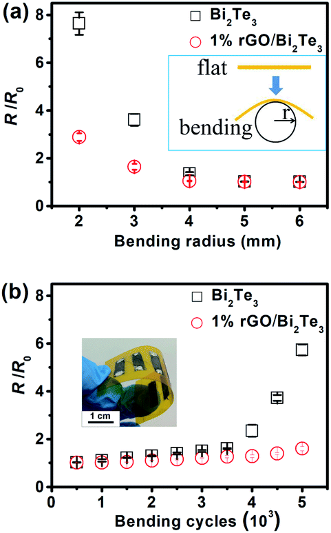 | ||
| Fig. 5 Flexibility testing: the change rate of the electrical resistance of pure Bi2Te3 nanoplates and 1% rGO/Bi2Te3 composite-based TEG devices as a function of different bending radius (a) and bending cycles (b) on 5 mm in bending radius, R0 and R are resistances of devices before and after bending. Error bars are estimated from repeatability of the experimental results: for each condition, three samples are prepared and measured. The R of 1% rGO/Bi2Te3 device increases by 2% after 1000 bending cycles with 5 mm of bending radius, while that of Bi2Te3 device increases about 10%. It reveals that the addition of rGO improved the flexibility of 1% rGO/Bi2Te3 device. | ||
Putting the comparison aside, the changes of R for both pure Bi2Te3 and 1% rGO/Bi2Te3 device are within 10% after 1000 bending cycles with 5 mm of bending radius. This result shows the good electrical stability of the two devices. We believe the reasons are like this: firstly, the suitable thickness of thermal elements (about 40 μm) prevents the thermal elements from cracking during bending. Secondly, the soft copper wires rather than some deposited metal layers are served as the connection material and these copper wires, which connect thermal elements end to end, have excellent resistance to bend. All these structural designs of the devices contribute to the stable electrical properties during bending.
Compared with other related literature shown in Table 2, our rGO/Bi2Te3 TEG device with just six planar thermal elements possesses good power output, which should be further increased with an increasing number of thermal elements. Moreover, our TEG device shows excellent flexibility, thanks to the good flexibility of both rGO/Bi2Te3 elements and the soft connection of thermal elements.
| Materials | S 2 σ, μW cm−1 K−2 | Element number | P max at various ΔT | V oc at various ΔT | Thickness of elements | Bending radius | Bending times/increase percentage of resistance |
|---|---|---|---|---|---|---|---|
| This work | 3.2–4.6 | 6 | 20 K: 1.72 μW | 20 K: 14 mV | 40 μm | 5 mm | 1000 cycles/2% |
| 60 K: 15.22 μW | 60 K: 45 mV | ||||||
| Bi2Te2.8Se0.2 film11 | 4.68 | 5 | 20 K: 0.4 μW | 20 K: 12 mV | 10 μm | 7 mm | 150 cycles/1.4% |
| 60 K: 6.1 μW | 60 K: 41 mV | ||||||
| Bi2Te3 film9 | 2–3.4 | 62 | 20 K: 25 μW | 20 K: 210 mV | 120 μm | — | — |
| Carbon nanotube1 | 15 | 3 p–n couples | 27.5 K: 2.51 μW | 27.5 K: 11 mV | 150 μm | — | — |
| WS2 (n-type) | WS2: 0.05 | 3 p–n couples | 60 K: 2.58 nW | 60 K: 13 mV | 100 nm | — | — |
| NbSe2 (p-type)4 | NbSe2: 0.26 | ||||||
| RGO/Bi2Te3(n-type) and SWCNTs/Sb2Te3 (p-type)43 | RGO/Bi2Te3: 1.08 | 10 couples | 70 K: 23.6 μW | 70 K: 135 mV | 25–30 μm | 1.8 mm | 800 cycles/25% |
| SWCNTs/Sb2Te3: 0.5 | |||||||
| PEDOT-Tos/TTF-TCNQ46 | 3.24 | 54 | 10 K: 0.128 μW | — | 3–30 μm | — | — |
| PEDOT:PSS47 | 2.84 | 16 | 10 K: 10.59 nW | 10 K: 12.75 mV | 1.1 mm | — | — |
| CNT/P3HT48 | 3.25 | 41 | 10 K: 32.7 nW | 10 K: 41.8 mV | 1.1–1.5 mm | — | — |
| Bi2Te3/CF49 | 2.5–3.75 | 12 pairs | 15 K: 0.2 μW | 15 K: 2 mV | 30 μm | 4 mm | 100 cycles/6% |
| Bi2Te3 (n-type) and Bi0.5Sb1.5Te3 (p-type) NWs50 | 1.8 | 5 pairs | 32.5 K: 127 nW | 32.5 K: 45 mV | 0.62–0.89 μm | 11 mm | 50 cycles/2.5% |
| SWCNT/PEDOT:PSS coated Te nanorod51 | 1.04 | 6 | 44 K: 53.6 nW | 44 K: 5.6 mV | 10 μm | — | — |
| Bi2Se0.3Te2.7 (n-type) and Bi0.5Sb1.5Te3 (p-type)/paper composite52 | Bi2Se0.3Te2.7: 0.44 | 10 p–n couples | 35 K: 10 nW | 35 K: 8 mV | 200 μm | 20 mm | 1000 cycles/<5% |
| Bi0.5Sb1.5Te3: 0.11 | |||||||
| BiSbTe films with 8 wt% Te53 | 3 | 4 | 80 K: 54 μW | 80 K: 64 mV | 27 μm | 10 mm | 1000 cycles/3% |
| Bi2Te3-based inorganic paints54 | 5 couples | 50 K: 60.7 μW | 50 K: 79.4 mV | 50 μm | — | — | |
| Bi2Te3-based inks55 | — | — | 39 K: 1.62 mW | 39 K: 27 mV | 1.5–2.0 mm | — | — |
Conclusions
In summary, high-performance flexible TEG devices are successfully constructed by a systematic strategy including the selection of rGO/Bi2Te3 composites as active materials, design of thickness of thermal elements, artful connection manner, and the adoption of a simple printing method. The Pmax of the TEG devices on flexible polyimide substrates made from 1% rGO/Bi2Te3 composites is considerably enhanced to 1.72 μW at ΔT = 20 K, compared with 1.45 μW at ΔT = 20 K for pure Bi2Te3 nanoplate based TEG devices. Furthermore, Pmax of the 1% rGO/Bi2Te3 composite based TEG devices is up to 15.22 μW at ΔT = 60 K. Significantly, the electrical resistance of the 1% rGO/Bi2Te3 composite based TEG devices merely changes by 2% after bending 1000 cycles on 5 mm in bending radius, which discloses good flexibility. The thermal elements are all n-type, next efforts will be made on solution-processed p-type materials with good ZT value, and a TEG device with several n–p thermal couples would be printed for higher power output. These inorganic-based TEGs with both high performance and good flexibility will largely promote the application of functional inorganic materials into flexible electronics through a mild wet-chemical method combined with compositional and structural design.Conflicts of interest
There are no conflicts to declare.Acknowledgements
The authors acknowledge financial support from by the National Basic Research Program of China (973 Program, 2015CB932600), the National Key R&D Program of China (2017YFA0208000), the National Natural Science Foundation of China (21525523, 21802130, 21874121, 21722507 and 21574048), the National Key Basic Research Program of China (2014CB931801 and 2016YFA0200700, Z. Y. T.), National Natural Science Foundation of China ( 21475029 and 91427302, Z. Y. T.), Frontier Science Key Project of the Chinese Academy of Sciences (QYZDJ-SSW-SLH038, Z. Y. T.), Instrument Developing Project of the Chinese Academy of Sciences (YZ201311, Z. Y. T.), CAS-CSIRO Cooperative Research Program (GJHZ1503, Z. Y. T.), “Strategic Priority Research Program” of Chinese Academy of Sciences (XDA09040100, Z. Y. T.) and K. C. Wong Education Foundation, Fundamental Research Funds for the Central Universities, China University of Geosciences (Wuhan) (No. CUG170669).References
- W. B. Zhou, Q. X. Fan, Q. Zhang, L. Cai, K. W. Li, X. G. Gu, F. Yang, N. Zhang, Y. C. Wang, H. P. Liu, W. Y. Zhou and S. S. Xie, Nat. Commun., 2017, 8, 1 CrossRef CAS PubMed.
- Z. Li, C. Xiao, H. Zhu and Y. Xie, J. Am. Chem. Soc., 2016, 138, 14810 CrossRef CAS PubMed.
- C. H. Zhang, Z. P. Peng, Z. Li, L. G. Yu, K. A. Khor and Q. H. Xiong, Nano Energy, 2015, 15, 688 CrossRef CAS.
- J. Y. Oh, J. H. Lee, S. W. Han, S. S. Chae, E. J. Bae, Y. H. Kang, W. J. Choi, S. Y. Cho, J. O. Lee, H. K. Baik and T. Il Lee, Energy Environ. Sci., 2016, 9, 1696 RSC.
- S. K. Li, T. J. Fan, X. R. Liu, F. S. Liu, H. Meng, Y. D. Liu and F. Pan, ACS Appl. Mater. Interfaces, 2017, 9, 3677 CrossRef CAS PubMed.
- C. Xiao, K. Li, J. J. Zhang, W. Tong, Y. W. Liu, Z. Li, P. C. Huang, B. C. Pan, H. B. Su and Y. Xie, Mater. Horiz., 2014, 1, 81 RSC.
- B. A. Xu, T. L. Feng, M. T. Agne, L. Zhou, X. L. Ruan, G. J. Snyder and Y. Wu, Angew. Chem., Int. Ed., 2017, 56, 3546 CrossRef CAS PubMed.
- C. H. Zhang, H. Ng, Z. Li, K. A. Khor and Q. H. Xiong, ACS Appl. Mater. Interfaces, 2017, 9, 12501 CrossRef CAS PubMed.
- D. Madan, Z. Q. Wang, A. Chen, R. C. Juang, J. Keist, P. K. Wright and J. W. Evans, ACS Appl. Mater. Interfaces, 2012, 4, 6117 CrossRef CAS PubMed.
- J. Hirotani, S. Kishimoto and Y. Ohno, Nanoscale Adv., 2019, 1, 636 RSC.
- T. Varghese, C. Hollar, J. Richardson, N. Kempf, C. Han, P. Gamarachchi, D. Estrada, R. J. Mehta and Y. L. Zhang, Sci. Rep., 2016, 6, 1 CrossRef PubMed.
- S. R. Tulsani, A. K. Rath and D. J. Late, Nanoscale Adv., 2019, 1, 1387 RSC.
- C. B. Vining, Nat. Mater., 2009, 8, 83 CrossRef CAS PubMed.
- G. J. Snyder and E. S. Toberer, Nat. Mater., 2008, 7, 105 CrossRef CAS PubMed.
- S. S. Zhou, L. Gan, D. L. Wang, H. Q. Li and T. Y. Zhai, Nano Res., 2018, 11, 2909 CrossRef CAS.
- S. Shin, R. Kumar, J. W. Roh, D. S. Ko, H. S. Kim, S. I. Kim, L. Yin, S. M. Schlossberg, S. Cui, J. M. You, S. Kwon, J. L. Zheng, J. Wang and R. K. Chen, Sci. Rep., 2017, 7, 7317 CrossRef PubMed.
- C. L. Ou, A. L. Sangle, A. Datta, Q. S. Jing, T. Busolo, T. Chalklen, V. Narayan and S. Kar-Narayan, ACS Appl. Mater. Interfaces, 2018, 10, 19580 CrossRef CAS PubMed.
- F. Suarez, D. P. Parekh, C. Ladd, D. Vashaee, M. D. Dickey and M. C. Ozturk, Appl. Energy, 2017, 202, 736 CrossRef.
- J. Gao, C. Y. Liu, L. Miao, X. Y. Wang, Y. Peng and Y. Chen, RSC Adv., 2016, 6, 31580 RSC.
- A. C. Arias, J. D. MacKenzie, I. McCulloch, J. Rivnay and A. Salleo, Chem. Rev., 2010, 110, 3 CrossRef CAS PubMed.
- Y. G. Sun and J. A. Rogers, Adv. Mater., 2007, 19, 1897 CrossRef CAS.
- Z. Y. Lin, Y. Chen, A. D. Yin, Q. Y. He, X. Q. Huang, Y. X. Xu, Y. A. Liu, X. Zhong, Y. Huang and X. F. Duan, Nano Lett., 2014, 14, 6547 CrossRef CAS PubMed.
- S. R. Thomas, P. Pattanasattayavong and T. D. Anthopoulos, Chem. Soc. Rev., 2013, 42, 6910 RSC.
- D. F. Ding, D. W. Wang, M. Zhao, J. W. Lv, H. Jiang, C. G. Lu and Z. Y. Tang, Adv. Mater., 2017, 29, 1 Search PubMed.
- C. Han, Z. Li, G. Q. Lu and S. X. Dou, Nano Energy, 2015, 15, 193 CrossRef CAS.
- C. Han, Q. Sun, Z. X. Cheng, J. L. Wang, Z. Li, G. Q. Lu and S. X. Dou, J. Am. Chem. Soc., 2014, 136, 17626 CrossRef CAS PubMed.
- C. Han, Q. Sun, Z. Li and S. X. Dou, Adv. Energy Mater., 2016, 6, 1600498 CrossRef.
- C. L. Wan, X. K. Gu, F. Dang, T. Itoh, Y. F. Wang, H. Sasaki, M. Kondo, K. Koga, K. Yabuki, G. J. Snyder, R. G. Yang and K. Koumoto, Nat. Mater., 2015, 14, 622 CrossRef CAS PubMed.
- S. J. Kim, J. H. We and B. J. Cho, Energy Environ. Sci., 2014, 7, 1959 RSC.
- C. Han, Z. Li and S. X. Dou, Chin. Sci. Bull., 2014, 59, 2073 CrossRef CAS.
- W. Glatz, S. Muntwyler and C. Hierold, Sens. Actuators, A, 2006, 132, 337 CrossRef CAS.
- S. Hong, Y. Gu, J. K. Seo, J. Wang, P. Liu, Y. S. Meng, S. Xu and R. K. Chen, Sci. Adv., 2019, 5, eaaw0536 CrossRef PubMed.
- S. Hong, S. Shin and R. Chen, Adv. Funct. Mater., 2020, 30, 1909788 CrossRef CAS.
- C. S. S. Sandeep, J. M. Azpiroz, W. H. Evers, S. C. Boehme, I. Moreels, S. Kinge, L. D. A. Siebbeles, I. Infante and A. J. Houtepen, ACS Nano, 2014, 8, 11499 CrossRef CAS PubMed.
- Y. X. Xu, H. Bai, G. W. Lu, C. Li and G. Q. Shi, J. Am. Chem. Soc., 2008, 130, 5856 CrossRef CAS PubMed.
- X. M. Li, J. Yin, J. X. Zhou, Q. Wang and W. L. Guo, Appl. Phys. Lett., 2012, 100, 183108 CrossRef.
- Y. Zhao, G. S. Tang, Z. Z. Yu and J. S. Qi, Carbon, 2012, 50, 3064 CrossRef CAS.
- H. R. Yang, J. H. Bahk, T. Day, A. M. S. Mohammed, G. J. Snyder, A. Shakouri and Y. Wu, Nano Lett., 2015, 15, 1349 CrossRef CAS PubMed.
- H. Ju and J. Kim, Dalton Trans., 2015, 44, 11755 RSC.
- R. Pasricha, S. Gupta and A. K. Srivastava, Small, 2009, 5, 2253 CrossRef CAS PubMed.
- H. Ju, M. Kim and J. Kim, J. Mater. Sci.: Mater. Electron., 2016, 27, 3427 CrossRef CAS.
- G. Anoop, J. R. Rani, J. Lim, M. S. Jang, D. W. Suh, S. Kang, S. C. Jun and J. S. Yoo, Sci. Rep., 2016, 6, 1 CrossRef PubMed.
- B. Wu, Y. Guo, C. Y. Hou, Q. H. Zhang, Y. G. Li and H. Z. Wang, Adv. Funct. Mater., 2019, 29, 1900304 CrossRef.
- S. Shin, J. W. Roh, H. S. Kim and R. K. Chen, J. Appl. Phys., 2018, 123, 205106 CrossRef.
- D. Chen, L. H. Tang and J. H. Li, Chem. Soc. Rev., 2010, 39, 3157 RSC.
- O. Bubnova, Z. U. Khan, A. Malti, S. Braun, M. Fahlman, M. Berggren and X. Crispin, Nat. Mater., 2011, 10, 429 CrossRef CAS PubMed.
- E. J. Bae, Y. H. Kang, K. S. Jang and S. Y. Cho, Sci. Rep., 2016, 6, 1 CrossRef PubMed.
- C. T. Hong, Y. H. Kang, J. Ryu, S. Y. Cho and K. S. Jang, J. Mater. Chem. A, 2015, 3, 21428 RSC.
- Q. Jin, W. B. Shi, Y. Zhao, J. X. Qiao, J. H. Qiu, C. Sun, H. Lei, K. P. Tai and X. Jiang, ACS Appl. Mater. Interfaces, 2018, 10, 1743 CrossRef CAS PubMed.
- B. L. Chen, M. Kruse, B. Xu, R. Tutika, W. Zheng, M. D. Bartlett, Y. Wu and J. C. Claussen, Nanoscale, 2019, 11, 5222 RSC.
- Q. F. Meng, K. F. Cai, Y. Du and L. D. Chen, J. Alloys Compd., 2018, 778, 163 CrossRef.
- X. Zhao, W. J. Han, C. S. Zhao, S. Wang, F. G. Kong, X. X. Ji, Z. Y. Li and X. A. Shen, ACS Appl. Mater. Interfaces, 2019, 11, 10301 CrossRef CAS PubMed.
- T. Varghese, C. C. Dun, N. Kempf, M. Saeidi-Javash, C. Karthik, J. Richardson, C. Hollar, D. Estrada and Y. L. Zhang, Adv. Funct. Mater., 2019, 30, 1905796 CrossRef.
- S. H. Park, S. Jo, B. Kwon, F. Kim, H. W. Ban, J. E. Lee, D. H. Gu, S. H. Lee, Y. Hwang, J. S. Kim, D. B. Hyun, S. Lee, K. J. Choi, W. Jo and J. S. Son, Nat. Commun., 2016, 7, 13403 CrossRef CAS PubMed.
- F. Kim, B. Kwon, Y. Eom, J. E. Lee, S. Park, S. Jo, S. H. Park, B. S. Kim, H. J. Lm, M. H. Lee, T. S. Min, K. T. Kim, H. G. Chae, W. P. King and J. S. Son, Nat. Energy, 2018, 3, 301 CrossRef CAS.
Footnotes |
| † Electronic supplementary information (ESI) available: Experimental detail, some supporting characterizations about the rGO and devices, two tables about Hall testing results and state-of-art excellent examples of printed planar TEG devices, and a video that diplays the real time measurement of open circuit voltage (ΔT = 20 K) of the thermoelectric generator device made from pure Bi2Te3 nanoplates. See DOI: 10.1039/d0na00118j |
| ‡ These authors contributed equally. |
| This journal is © The Royal Society of Chemistry 2020 |