
 Open Access Article
 This Open Access Article is licensed under a
 Creative Commons Attribution 3.0 Unported Licence
The prospective application of a graphene/MoS2 heterostructure in Si-HIT solar cells for higher efficiency†
Chandra Kamal
Borah
a,
Pawan K.
Tyagi
bc and
Sanjeev
Kumar
 *a
*a
aCentre of Advanced Research, Department of Physics, Rajiv Gandhi University, Arunachal Pradesh-791112, India. E-mail: sanjeev.kumar@rgu.ac.in
bDepartment of Physics, Central University of Haryana, Haryana-123029, India
cDepartment of Applied Physics, Delhi Technological University, Delhi-110042, India
First published on 23rd June 2020
Abstract
The efficiency of a Si-HIT (heterojunction with intrinsic thin layer) solar cell based on a graphene/MoS2 heterostructure has been optimized by varying the various parameters of graphene (Gr) as a transparent conducting electrode (TCE) and n-type molybdenum disulfide (n-MoS2) as an emitter layer. The photovoltaic performance of a graphene/n-MoS2/a-Si:H/p-cSi/Au single facial HIT solar cell has been studied using AFORS-HET v2.5 simulation software. A maximum output efficiency of 25.61% has been achieved. The obtained results were compared with the results from a commercially available a-Si:H layer and p-cSi wafer after simulation. Moreover, the dependence of the cell performance on changes in the TCE and the back contact materials has also been studied. Finally, it has been demonstrated that the graphene layer and n-MoS2 layer could act as a TCE and an efficient emitter layer, respectively, in a n-MoS2/p-cSi based HIT solar cell.
1. Introduction
The output efficiency (η) of a simple silicon (Si) heterojunction solar cell degrades owing to the presence of a large number of defects at the surface of the Si wafer. This deficiency of heterojunction solar cells can be overcome by the introduction of a thin intrinsic layer between the two doped layers of the heterojunction. Such a structure is known as a heterojunction with intrinsic thin layer (HIT) structure.1 In a HIT structured solar cell, the intrinsic layer-like a-Si:H reduces the interfacial recombination state density to the minimum level between two doped layers2 and reduces the leakage current.3 Recently, SANYO Ltd reported attaining a 20% output efficiency in HIT solar cells based on n-type Si.4 Furthermore, Panasonic has achieved the world's highest efficiency of 25.6% in a HIT cell based on an n-type c-Si.5In a solar cell, a transparent conductive electrode (TCE) is required to ensure the easy transportation of carriers from the emitter layer to the external circuit. The low sheet resistance (10 Ω sq−1) and high optical transparency (85%) mean that indium tin oxide (ITO) is a commonly used TCE in photovoltaic (PV) applications. However, the high cost, rarity and mechanical rigidity of ITO have limited its use for future flexible devices and these drawbacks initiated the search for new TCE materials.6 Recently, pristine graphene has been reported to have an optical transparency as high as 97.7% (single layer graphene) with a work function of 4.31–4.5 eV (ref. 7 and 8) and a sheet resistance of 120 Ω sq−1 in few-layer graphene.6 In addition, the intercalated graphene with ferric chloride is reported to have a high optical transparency of approximately 96% with a low sheet resistance of 8.8 Ω sq−1 and a high carrier density of 8.9 × 1014 cm−2 at room temperature and a high stability in air.6 At room temperature, the carrier mobility in the graphene layer exceeds 105 cm2 V−1 s−1.9 These extraordinary properties have led to the application of multilayer graphene as a TCE. Recently, Lazar et al.7 reported that doping with boron (B) and –NH2 can increase the work function of graphene (ΦGr) to 1.20 eV and 0.46 eV from 4.31 eV (pristine graphene). Kim et al.8 demonstrated that, after being irradiated by an α beam the work function of graphene increases to 4.9 eV. Conversely, the low photoresponsivity, poor external quantum efficiency, and low absorption of light reduces the application of graphene as an emitter layer instead of the TCE layer in HIT solar cell.10 Unlike graphene, another 2D material, molybdenum disulfide (MoS2) has emerged as a complement 2D material for graphene as an emitter layer in HIT solar cells. MoS2 has a mobility of 200 cm2 V−1 s−1 in the monolayer and approximately 517 cm2 V−1 s−1 in few layers, as well as a high on/off ratio in the order of 108 (ref. 11 and 12) and a fast photo-response time of 40 μs.13 MoS2 is reported to have an indirect bandgap of 1.2 eV in the bulk form and a direct bandgap of 1.9 eV in the single layer form.14 Moreover, double layer MoS2 has more than 85% optical transparency in the visible region.15 Recently, it has been reported that the work function of MoS2 changes with a change in the number of layers.16 It has also been demonstrated that MoS2 can be used to form significant n-type doping with a Benzyl Viologen (BV) dopant17 and polyethyleneimine (PEI)18. PEI reduces the sheet resistance of MoS2 2.6 times.18 These properties mean that MoS2 can be utilized as an emitter layer in MoS2/silicon HIT solar cells.
Experimentally and theoretically, it has been demonstrated that MoS2 can act as an emitter layer in heterojunction silicon solar cells. Tsai et al.19 fabricated a heterojunction solar cell of monolayer MoS2 and p-cSi and achieved a power conversion efficiency of 5.23%. Hao et al.20 also fabricated a bulk p–n junction after depositing a 40 nm thick layer of n-MoS2 onto p-cSi substrates and a 1.3% photoconversion efficiency was achieved.
The high transparency, as well as the high mobility of the graphene layer with a tunable bandgap and work function, along with practical and theoretical demonstrations of graphene/MoS2 and MoS2/Si heterojunctions, motivated us to propose a single facial HIT solar cell structure of graphene/n-MoS2/a-Si:H/p-cSi/Au. Here, we have used graphene as a TCE material. No reports have been published on the use of graphene as a TCE in HIT solar cells so far. In addition to graphene and MoS2, there are a few interesting candidates such as carbon nanotubes, black phosphorous and MXene, that show potential for use in silicon solar cells. So far, a power conversion as high as 17.2% has been observed in carbon nanotube based silicon solar cells.21–23 After proposing the structure of the cell, the influence of various parameters of the layers used on the cell performance were studied using AFORS-HET v2.5 simulation software. The main objective of the present simulation is to study the independent effects owing to the variation of the parameters of the layers on the cell performance and to demonstrate the prospective application of graphene as an effective TCE material in a n-MoS2/p-cSi HIT solar cell.
2. Physical model, structural model and formation of the junctions
2.1 Physical model
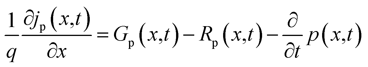
AFORS-HET is solar cell simulation software, used to study and analyze the various properties of a heterojunction solar cell. For the proposed structure, this software solves Poisson's equation and the transport equation for electrons and holes in one dimension. These equations are as follows: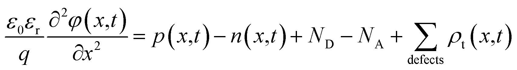
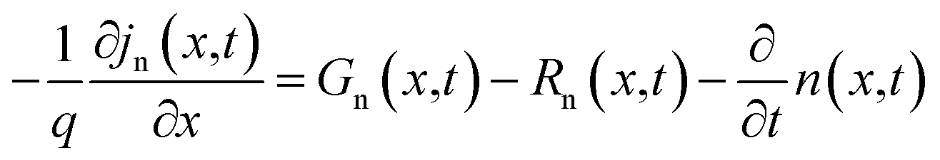
In which, n represents the electron density, p is the hole density, φ is the electric potential, q is the electron charge, ε0εr is the absolute/relative dielectric constant, and ND/A represents the donors/acceptors concentrations, which are assumed to be completely ionized. Here, n, p and φ are the independent variables for which the system of differential equations is solved.
The charge stored in the defects is described by a distribution function, ft, specifying the probability that defects with a defect density Nt are at position E if the bandgap is occupied with electrons:


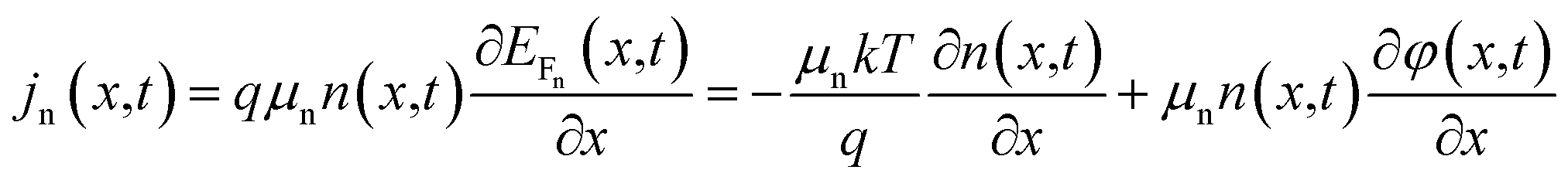
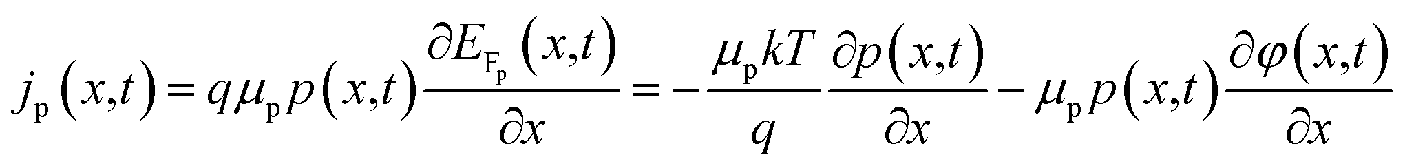
The electron/hole currents (jn/p) flow owing to the gradient of the corresponding quasi-Fermi energy (EFn/p). Within the semiconducting layer, this is equivalent to the sum of the diffusion and drift current with the corresponding mobility μn/p.
If the heterostructure is illuminated (specifying the spectral distribution ϕ(λ) of the incoming photon flux), the super-bandgap optical generation rate  from the valence band into the conduction band of the semiconductor layers can be evaluated by considering the Lambert–Beer absorption model by specifying the spectral absorption coefficient α, as well as specifying the dielectric properties (n,k) of each layer. An optical sub-bandgap generation
  from a defect to the conduction/valence band can be defined by specifying the optical emission coefficients eon(E),eop(E) ≠ 0 for the defect state.
Recombination from the conduction band into the valence band may occur directly (band to band recombination, Auger recombination) and via trap states (Shockley–Read–Hall recombination, (SHR)).
| Rn,p(x,t) = RBand–Bandn,p(x,t) + RAugern,p(x,t) + RSRHn,p(x,t) |
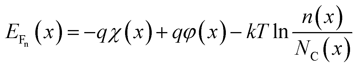
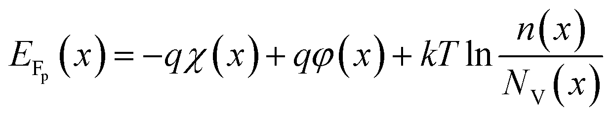
The transportation across the heterojunction interface is modeled by drift-diffusion. In order to do so, an interface layer is considered. The specified interface defects are distributed homogeneously within this layer. The cell currents have to be evaluated directly from the gradient of the corresponding quasi-Fermi energies. The electron affinity (χ), the bandgap (Eg) and the effective conduction/valence band density of states (NC, NV) will depend on the position x within the interface layer.
The electric potential is fixed to zero at one contact. At the second contact, a boundary condition has to be specified, which relates the external cell voltage/current to the internal quantities. Furthermore, the electron and hole currents moving into the metal contacts need to be modeled. The Schottky contact can either be voltage controlled, or current controlled.
2.2. Structural model
Layered structure MoS2 can be directly deposited on Si substrates. However, owing to their structural mismatch (i.e. layered structure of MoS2 and diamond-like structure of Si), large quantities of lattice defects are produced and this increases the recombination at the interface. Thus, the introduction of an intrinsic (i) buffer layer a-Si:H could be beneficial to balance the carrier injection and reduce the leakage current in the cell.3 Therefore, the as-synthesized MoS2 is an n-type semiconductor24 and p-type silicon is more popular in the PV industries.4 Thus, in this simulation, we have used p-cSi as a base material. Moreover, the minority carrier diffusion length in p-cSi is also reported to be higher than n-cSi.25 Furthermore, Fan et al.26 have reported that ultrathin gold (Au) contacts provide a better electrical conductivity and optical reflectance-scattering to maintain the performance of the cell compared with ITO. Also, it has been demonstrated that an Au/Si interface formed by using novel transfer printing technology makes excellent electrical contact and exhibits a low contact resistance in comparison to that formed by vacuum deposition of Au on Si.27 Therefore, the proposed structure of the single facial HIT solar cell is configured as graphene/n-MoS2/a-Si:H(i)/p-cSi/Au, as shown in Fig. 1. No lattice mismatch between the layers has been considered for this simulation. Ideally, a semiconductor is called 2D if it satisfies the condition 〈t〉 ≤ λF, in which 〈t〉 is the average system of the 2D electron system, λF is the Fermi wavelength which is equal to nm, and n2D is the carrier density in cm−2.28 Following this condition as reported by Sarma et al.29 and Suh et al.30 even n ∼ 105 cm−3 in graphene and n ∼ 1.8 × 1014 cm−3 in MoS2 cannot satisfy the above described conditions respectively. It has also been reported that doping in 2D materials increases the interlayer spacing.31 Thus, we consider graphene and MoS2 quasi 3D in nature instead of 2D. The quantum confinement in the structure was achieved by controlling the layer number of n-MoS2. In the proposed HIT structure, as shown in Fig. 1a the carrier transport occurred along the c-axis. Details of the front contact and the back contact parameters of the proposed structure are given in Table 16,7,26,32–37 and the parameters, as well as the ranges of the n-MoS2, a-Si:H and p-cSi are given in Table 2. The thickness of the single graphene was taken as 0.334 nm and the monolayer MoS2 as 0.65 nm.19,38,39 However, we started our simulation from five-layer (5L) graphene (1.67 nm) and six-layer (6L) MoS2 (3.9 nm) by considering the high overlapping probability of the graphene and p-cSi. It was also reported that the Raman spectrum of 6L MoS2 is very close to the bulk37 and the optical transparency of 5L graphene (88.5%) is more than that of ITO (85%).6 The parameters considered for optimization of the MoS2 layer were the donor concentration (ND), NC/NV, Eg, layer thickness, χ, dielectric constant (εr) and electron mobility (μn). The values of these parameters were kept within range and these and the results of the above mentioned previous literature are tabulated in Table 2.3,40–47 To simulate and optimize the other parameters the bulk and interfacial defect distribution and recombination rates were kept constant in the software. Furthermore, the MS-Schottky contact model was selected for the graphene/n-MoS2 and p-cSi/Au interfaces and the drift-diffusion model was selected for the n-MoS2/a-Si:H and a-Si:H/p-cSi interfaces. The values and parameters of these interfaces48 are listed in Table 3. The values of these parameters were varied accordingly under air mass 1.5 (AM1.5) illuminations under a power density of 100 mW cm−2 and a temperature of 300 K. In order to study the effect of the layer parameters on the cell performance, the open-circuit voltage (VOC), short circuit current density (JSC), fill factor (FF) and efficiency (η) were analyzed. After optimizing the parameters of n-MoS2 further simulation was extended to the a-Si:H layer and the thickness and bandgap were optimized. The values and ranges of these parameters were obtained from previously published studies.4,49–51 Further simulations were performed to optimize the parameters, such as the NA, NC/NV, χ, and thickness for p-cSi. The values and the ranges of the parameters for the p-cSi layer were taken from the previously published research.4,47and48 The defect properties were kept as the default. Finally, we optimized the parameters of the contact materials, that is graphene, Au, ITO, Ag, and so forth. The work function (Φ) and the number of layers were optimized and other parameters were fixed, as found in the literature.7,8,34–37,52
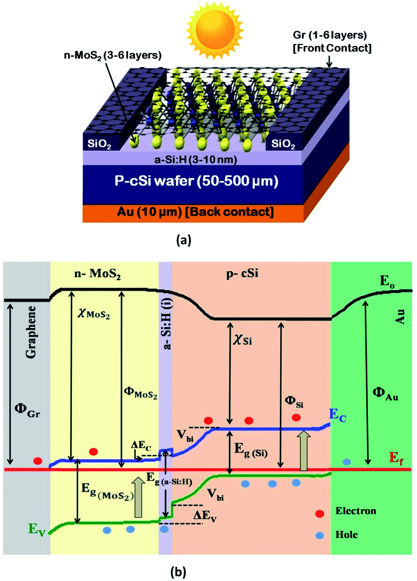 | ||
| Fig. 1 (a) The proposed HIT solar cell structure, and (b) band diagram as generated using AFORS-HET software for the proposed structure. | ||
| Parameter | Front contact | Back contact | |||
|---|---|---|---|---|---|
| Initially | After optimization | Initially | After optimization | ||
| Material | Graphene | ITO | Al | Au | Ag |
| Thickness | 1L–5L (1L = 0.334 nm) | 80 nm | 80 nm | 10 μm | 10 μm |
| Optical properties | n = 2.7 | ITO nk (default) | n = 1.19 | Au nk (default) | Ag nk (default) |
| k = 1.45 | k = 7.05 | ||||
| Work function (eV) | 4.31 | 4.4 | 4.06 | 5.4 | 4.64 |
| 4.50 | 4.45 | 4.20 | 4.74 | ||
| 4.54 | 4.5 | 4.26 | |||
| 4.77 | |||||
| 4.90 | |||||
| Absorption loss | 0.023 (constant) | ITO abs (default) | 0.056 | 0 | 0 |
| External reflection | 1L = 0 | ITO Ref (default) | 0.868 | 0 | 0 |
| 2L = 0.023 | |||||
| 3L = 0.046 | |||||
| 4L = 0.070 | |||||
| 5L = 0.092 | |||||
| Surface condition | Plane | Plane | Plane | Plane | Plane |
| Internal reflection | 0 | 0 | 0 | 0 | 0 |
| Parameter | n-MoS2 | a-Si:H(i) | p-cSi |
|---|---|---|---|
| Thickness | 3L–6L (1L = 0.65 nm) | 3–10 nm | 50–500 μm |
| Dielectric constant (εr) | 4–14 | 11.9 | 11.9 |
| Electron affinity χ (eV) | 3.74–4.45 | 3.9 | 4.05 |
| Band gap, Eg (eV) | 1.41–1.48 | 1.6–2.0 | 1.12 |
| Effective conduction band density, NC (cm−3) | 3 × 10¹⁸ to 9 × 10²⁰ | 2.5 × 10²⁰ | 3 × 10¹⁹ to 1 × 10²¹ |
| Effective valence band density, NV (cm−3) | 3 × 10¹⁸ to 9 × 10²⁰ | 2.5 × 10²⁰ | 3 × 10¹⁹ to 1 × 10²¹ |
| Effective electron mobility, μn (cm2 V−1 s−1) | 517 | 20 | 1104 |
| Effective hole mobility, μp (cm2 V−1 s−1) | 8.5 | 5 | 420 |
| Acceptor concentration NA (cm−3) | 0 | 0 | 1015 to 1017 |
| Donor concentration ND (cm−3) | 1012 to 1018 | 0 | 0 |
| Electron thermal velocity, Ve (cm s−1) | 107 | 107 | 107 |
| Hole thermal velocity, Vh (cm s−1) | 107 | 107 | 107 |
| Layer density, (g cm−1) | 5.06 | 2.328 | 2.328 |
| Auger electron recombination coefficient, (cm6 s−1) | ∼10−24 | 0 | 2.2 × 10⁻³¹ |
| Auger hole recombination coefficient, (cm6 s−1) | ∼10−24 | 0 | 9.9 × 10⁻³² |
| Band-to-band recombination coefficient, (cm3 s−1) | ∼10−7 | 0 | 9.5 × 10⁻¹⁵ |
| Defect type | Single | Conduction tail | Single |
| Defect charge | Acceptor | Acceptor | Acceptor |
| Total defect density (cm−3) | 1018 | 6.4 × 10¹⁹ | 1010 |
| Specific defect density (cm−3 eV−1) | 1018 | 1.83 × 10²¹ | 1010 |
| Defect level energy (eV) | 0.6 | 0.035 (Urbach) | 0.56 |
| Electron and hole capture cross section (cm−2) | 10−14 (default) | 7 × 10⁻¹⁶ | 10−14 |
| Optical properties | n = 4.47; k = 1.01 | a-Si nk (default) | c-Si nk (default) |
| Interface | Numerical model | Remarks |
|---|---|---|
| Graphene/n-MoS2 | MS-Schottky contact | Surface recombination velocity for electrons and holes = 107 cm s−1 (default) |
| p-cSi/Au | ||
| n-MoS2/a-Si:H | Drift diffusion model | Interface charge = 1011 cm−2 |
| a-Si:H/p-cSi |
2.3 Formation of the junctions
If n-MoS2 and p-cSi are brought into contact, a heterojunction forms and bending of the energy bands occur close to the Fermi level. This built-in potential (Vbi) is developed at the MoS2/p-cSi interface. This voltage facilitates the separation of photo-generated carriers in the solar cell. Generally, in the p–n junction solar cell, the interfacial defect density reduces the overall efficiency of the cell. Therefore, better surface passivation between the two layers is required to reduce the defect density at the interface. Here, an intrinsic layer a-Si:H is inserted between n-MoS2 and p-cSi. This layer can be deposited on Si using the plasma-enhanced chemical vapor deposition method at a low temperature (<200 °C) without degrading the bulk properties of the Si substrate.4 Also, it introduces band offsets between the active and emitter band which are also beneficial to obstructing the reverse flow of the charge carriers. The schematic energy band diagram of the proposed HIT solar cell is shown in Fig. 1b. The build-in potential (eVbi) in the HIT solar cell is defined as: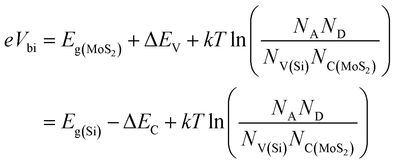 | (1) |
| eVbi = e(ΦMoS2 − ΦGr) | (2) |
3. Results and discussion
3.1 Consequences of the n-MoS2 layer
In this section, we have optimized the donor ND of the n-MoS2 layer in the range from 1012 to 1018 cm−3, and other parameters such as the thickness, NC/NV, Eg,χ and εr are kept at feasible values as shown in Fig. 2a and b. In Fig. 2b, it can be seen that as ND was increased from 1012 cm−3 to 1016 cm−3, the VOC remained constant at the value of 636.7 mV. At ND > 1016 cm−3, the VOC increased to 646.1 mV as ND was increased to 1018 cm−3. At a low value of ND, the consistency of VOC indicates that it does not depend on ND unless the condition Δno ≫ ND is followed, as reported previously,56 in which Δno represents the excess electron–hole pairs. At ND > 1016 cm−3, the VOC increases owing to enhancement in the eVbi according to eqn (2). As the mobility of the photo-generated carriers remains almost constant even with an increase of ND, this might keep JSC constant at 32.33 mA cm−2. Similarly, the FF was found to be constant at 76.71% until the ND reached 1016 cm−3 and then the FF slightly reduced to 75.73%. This is due to an increase in the recombination rate at a higher ND (1018 cm−3). As we have observed, the ND controls the VOC, thus the η of the cell remained constant at 15.79% as the ND increases, and a maximum of η = 15.82% was obtained at ND = 1018 cm−3.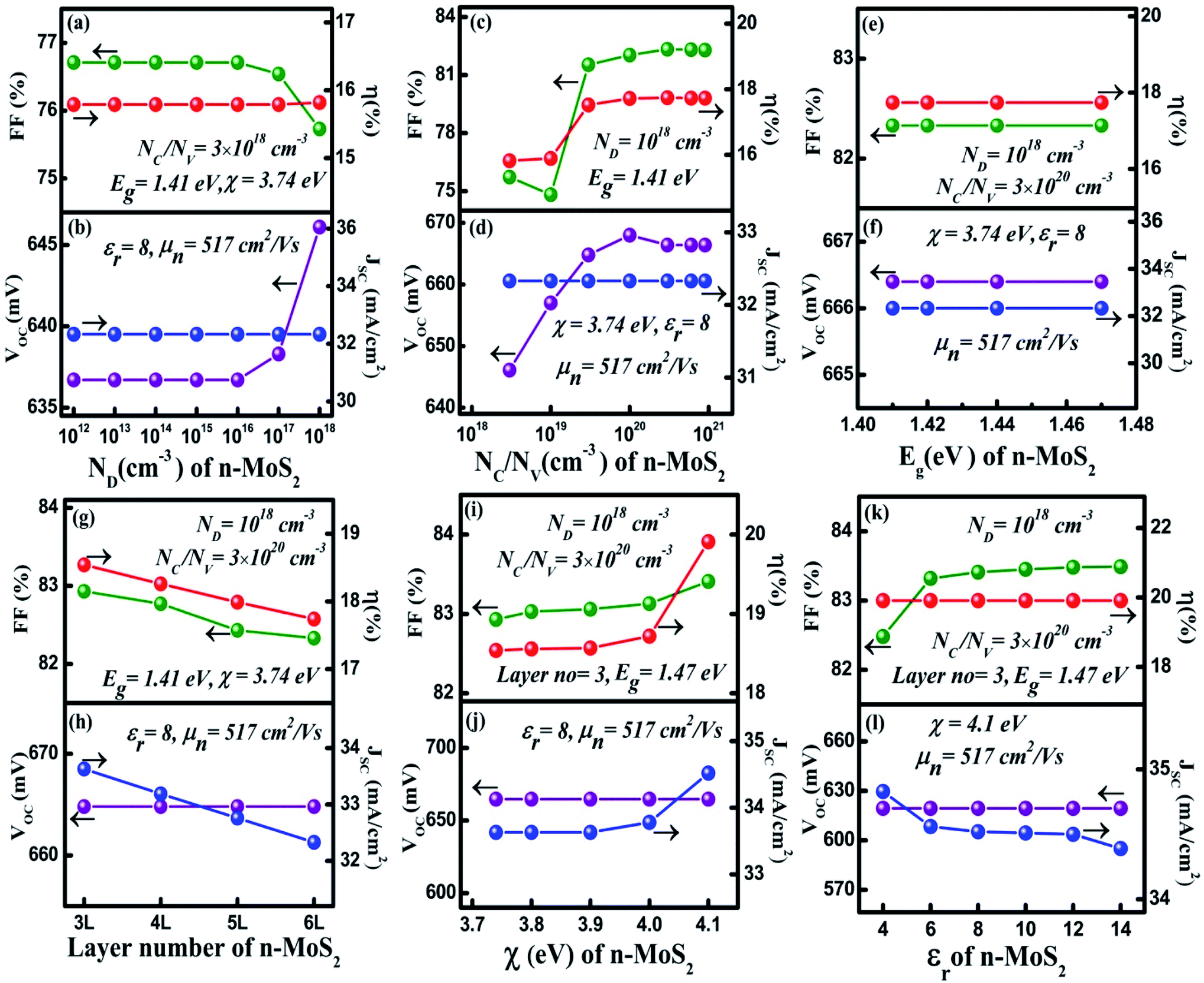 | ||
| Fig. 2 Optimization of the n-MoS2 layer: (a) and (b) donor concentration ND (cm−3), (c) and (d) effective conduction band and valance band density NC/NV (cm−3), (e) and (f) the bandgap energy Eg (eV), (g) and (h) the number of layers of MoS2, (i) and (j) the electron affinity χ (eV), and (k) and (l) the dielectric constant εr. The p-cSi parameters were maintained as: thickness = 100 μm, NA = 1 × 1016 cm−3, NC/NV = 3 × 1019 cm−3 and χ = 4.05 eV, and the graphene parameters were maintained as: number of layers = 5, reflectance = 0.092 and work function = 4.31 eV. The other parameters are given in Tables 1 and 2. | ||
The NC/NV is related to the effective mass of the electrons  and holes
  as follows:
 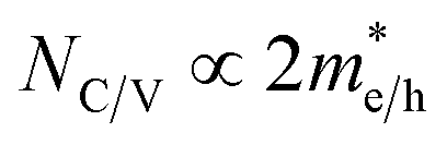 . Furthermore,
  is related to the mobility (μe/h) as follows:
 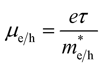 . From these two relationships, it can be concluded that with the change in mobility (μe/h) the conduction and valence band density (NC/NV) also changes. It has been reported that the mobility of the charge carriers in MoS2 changes with the change in the number of layer. MoS2 has a mobility of 200 cm2 V−1 s−1 in the monolayer and approximately 517 cm2 V−1 s−1 in few layers.11 Therefore, after optimization of ND to 1018 cm−3, the NC/NV was optimized in the range 3 × 10¹⁸ to 9 × 1020 cm−3 as shown in Fig. 2c and d. It can be seen in Fig. 2d that the VOC increased from 646.1 to 668 mV with an increase of the NC/NV from 3 × 1018 cm−3 to 1020 cm−3. The increment in VOC can be understood by considering the equation:
 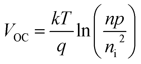 in which ni is the carrier concentration, n is the intrinsic electron concentration and p represents the intrinsic hole concentration. Here, n = no + Δn and p = po + Δp, in which no and po are the concentrations of the electrons and holes in the equilibrium condition and Δn, Δp are the excess photo-generated electron and hole concentrations, respectively. As, nopo = ni2, n = ND and Δn = Δp, VOC can therefore be rewritten as
 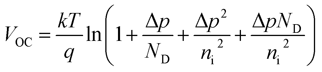 .57 We can assume that VOC increased with NC/NV owing to an increase of Δp and Δn. As shown in Fig. 2d, the VOC decreased a little bit to 666.4 mV as the NC/NV increased to 9 × 1020 cm−3, which is due to the decrement of eVbi according to eqn (1). The JSC was found to remain constant at 32.33 mA cm−2 with an increase of NC/NV from 3 × 10¹⁸ to 9 × 1020 cm−3. Although the generation rate (G) of the photo-generated carriers is reported to increase with higher values of NC/NV.58 The constant JSC indicates that the photo-generated carriers either recombine or are trapped close to the metal/semiconductor interface. As with the VOC, the FF is also found to increase and a maximum value of 82.33% was obtained at NC/NV = 3 × 1020 cm−3. Therefore, η was found to be enhanced from 15.82% to a maximum value of 17.73%.
After optimization of the ND and NC/NV to values of 1018 cm−3 and 3 × 1020 cm−3, respectively we varied the bandgap (Eg) in the range 1.41–1.47 eV (ref. 39) and results are shown in Fig. 2e and f. As we can see, all of the cell parameters are constant and a value of η = 17.74% was obtained in this range of Eg.
For the simulation with different numbers of layers of n-MoS2 as shown in Fig. 2g and h, the VOC was found to remain constant at a value of 664.8 mV, whereas the JSC reduced from 33.63 to 32.33 mA cm−2, when the number of layers was increased from 3 to 6. This happens because the increase in the number of layers reduces the transmittance of photons to reach the junction, which results in a reduction of the electron–hole pair generation rate. The reduction of the transmittance with the increase in the n-MoS2 layer number leads to a reduction of the FF. The η was found to decrease from 18.54% to 17.74% as the number of layers increased from 3 to 6. Hence, we used 3L as the optimized number of layers of MoS2 for further simulation.
Fig. 2i and j show the cell parameters for the optimization of χ in the ranges 3.7 to 4.1 eV. Here we have considered Eg = 1.47 eV for 3L MoS2.42 The VOC remained constant at a value of 664.8 mV when χ (eV) was increased from 3.7 to 4 eV. Upon a further increase in the χ to 4.1 eV, a small increase in the VOC to approximately 691.4 eV was obtained owing to an increase in the eVbi. A constant JSC of 33.63 mA cm−2 was found in the range 3.74–3.90 eV of χ and this was enhanced to 34.16 mA cm−2 for χ = 4.1 eV. A small increase in the ΔEC (see Fig. 1b) was observed with the increase in χ, which leads to a slightly higher VOC and JSC at χ = 4.1 eV. The FF was observed to increase from 82.93% (@ χ = 3.74 eV) to 83.41% (@ χ = 4.1 eV) as a result of the reduction in the sheet resistance. Therefore, η was found to increase from 18.54% to 19.19%.
It has been found from electric transportation measurements that the dielectric response of the MoS2 layers is sensitive to the substrate that is used and the dielectric effect relies on the thickness of the sample.43 The effect of the dielectric constant (εr) on the cell parameters is depicted in Fig. 2k and l. It can be observed in Fig. 2l, that the VOC does not depend on the variation of εr and it was found to be a constant at 691.4 eV. However, the JSC shows a light decrement from 34.83 to 34.39 mA cm−2 with an increase of εr up to 14. In a p–n junction, 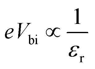 , which affect the relative permittivity of the MoS2 layer.54,57 The generation of the e–h pair increases in the MoS2 layer with an increase in the εr following Coulombs law as
 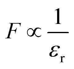 , in which F is the electrostatic force between the electron and holes, but at the same time the increase in εr reduces eVbi. As a consequence of both of these effects, we obtained a constant VOC. In contrast, under short circuit conditions, the photo-generated carriers experienced reduced eVbi, which boosts the recombination of the carriers. Thus, the JSC was found to decrease. The FF showed a minor increase from 82.43% to 83.41% when εr was increased from 4 to 6. After this the increase in FF slowed down and only reached 83.49% for εr = 14. In Fig. 2k, η was found to largely depend on the VOC and remained constant at 19.91% with εr. The cell parameters of the proposed cell were found to be independent of the electron mobility (μn) of the n-MoS2 layer, which has been varied in the range of 517–50 cm2 V−1 s−1.
3.2 Effect of the a-Si:H(i) layer thickness
In the HIT solar cell, an intrinsic layer of a-Si:H is inserted, mainly for passivation of the c-Si surface in the cell.51 Moreover, the insertion of the thin intrinsic layer also contributes to the depletion region, as well as to the drift current and electric field strength.59Fig. 3a and b shows the dependence of the cell parameters on the thickness variation of the a-Si:H(i) layer is in the 3 to 10 nm range. It can be observed in Fig. 3b that along with the increase of a-Si:H(i) thickness from 3 to 4 nm, the VOC was slightly enhanced from 691.4 to 693 mV owing to a minor increase in the barrier height at the a-Si:H(i) layer and p-cSi interface.43 The VOC then became constant at 693 mV upon further increasing the thickness of a-Si:H(i). The JSC was found to decrease linearly from 34.56 to 34.08 mA cm−2. It is reported that a thicker intrinsic layer increases the series resistance in the cell.50 Therefore, we observed a tiny change in the JSC. Thus, the FF was found to reduce from 83.32% to 82.43%. Consequently, the η obtained reduced from 19.91% to 19.51%. To observe the cell performance for the optimized bandgap energy of a-Si:H(i), a further simulation was carried out by varying the Eg a-Si:H(i) in the range 1.6 to 2 eV. However, the maximum η = 19.19% was only obtained at Eg = 1.6 eV. This might be because the absorption of the photons by the MoS2 layer only corresponds to this Eg of the a-Si:H(i) layer.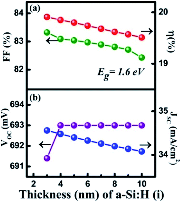 | ||
| Fig. 3 Optimization of the a-Si:H(i) layer: (a) and (b) thickness (nm) in which Eg was maintained at 1.6 eV. | ||
3.3 Optimization of the p-cSi layer
After optimizing the n-MoS2 and a-Si:H(i) parameters to their optimal values, the simulation was further performed to optimize the parameters of the p-cSi layer, while keeping the parameters of n-MoS2 and a-Si:H(i) at their optimal values, as discussed in the previous section. The results of the cell performance against variation in the NA variation of p-cSi are shown in Fig. 4a and b. It is observed in Fig. 4b that when the NA is increased from 1015 to 1017 cm−3, the VOC also increased from 691.2 to 699.2 mV owing to the higher eVbi with NA according to eqn (1). Similarly, JSC was also found to increase from 34.23 to 39.15 mA cm−2 as the increased eVb pushes the photo-generated carriers effectively from the depletion region into the contact region without experiencing a recombination effect or the charge carrier trapped effect in the neutral region. This resulted in an increment in the JSC.57 The increment in the FF from 81.48% to 82.76% can be attributed to the reduction of the sheet resistance as JSC is also increased. These changes lead to an improvement in η from 19.46% to 21.88%. Hence, NA = 1017 cm−3 with a maximum η of 21.88% is considered to be the optimal value for the c-Si layer.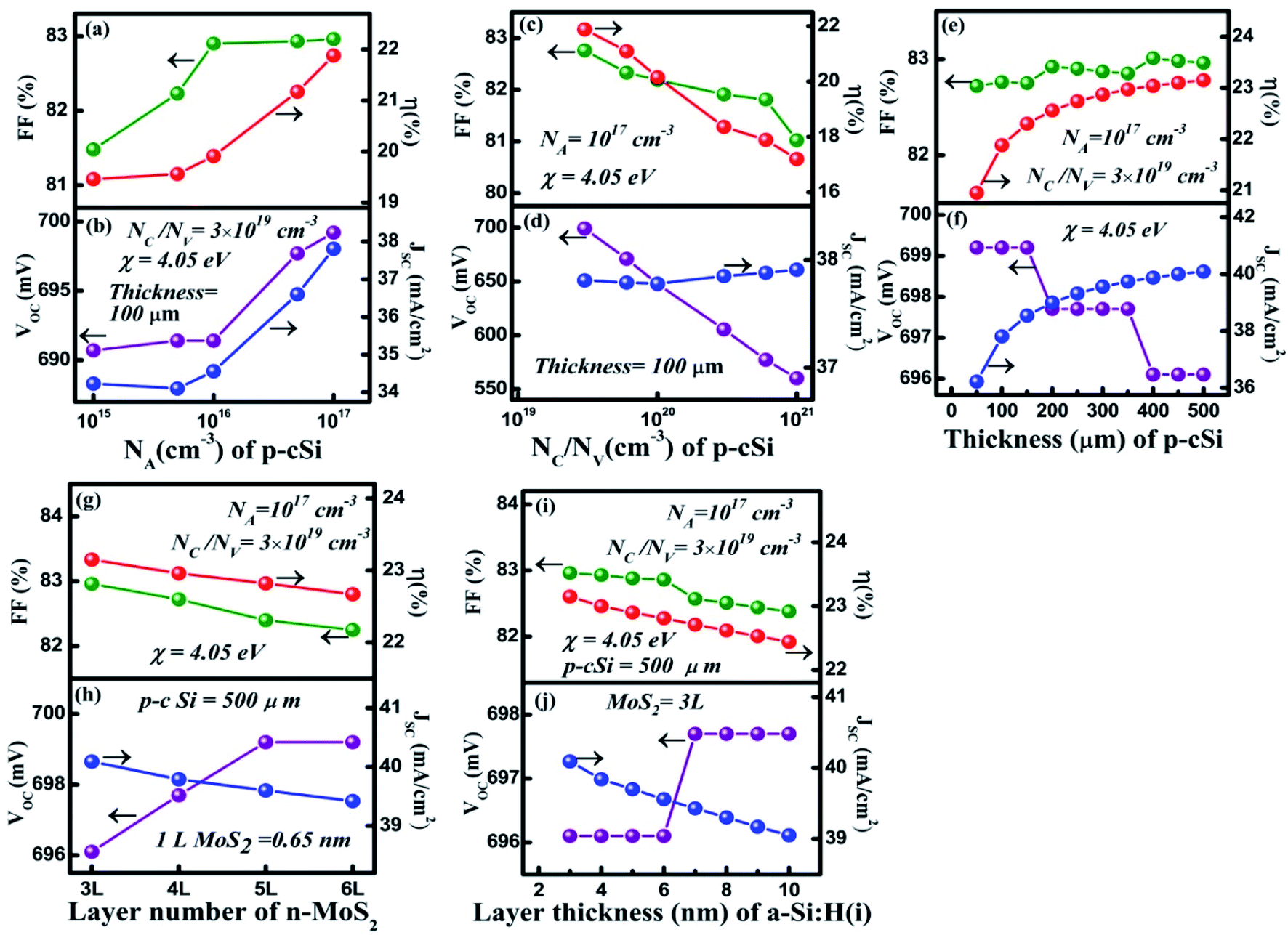 | ||
| Fig. 4 Optimization of the p-cSi layer: (a) and (b) acceptor concentration NA (cm−3), (c) and (d) effective conduction band and valance band density NC/NV (cm−3), (e) and (f) thickness (μm), (g) and (h) number of layers of MoS2 and (i) and (j) layer thickness of a-Si:H(i). The optimized parameters of a-Si:H(i) were maintained as: thickness = 3 nm, Eg = 1.6 eV, and the parameters for n-MoS2 were maintained as: ND = 1018 cm−3, NC/NV = 3 × 1020 cm−3, number of layers = 3, Eg = 1.47 eV, χ = 4.1 eV and εr = 6. | ||
To understand the effect of NC and NV on the performance of the HIT solar cell, we varied these parameters within the range of 3 × 10¹⁹ to 1 × 1021 cm−3 for the p-cSi layer. It can be observed from Fig. 4c and d, with the increase in the NC/NV, the VOC decreased linearly from 699.2 to 560.2 mV. According to eqn (1), with the increase in the NV of p-cSi layer the eVbi decreases and therefore VOC also decreases. In contrast, the value of JSC shows a small increase from 37.81 to 37.91 mA cm−2 with NC/NV. It has also been reported that NC/NV influences the bandgap as well as the absorption of photons.58 It can be estimated that for NC/NV > 3 × 1019 cm−3, the high absorption of photons in the active silicon layer increased the G of electron–hole pairs. In Fig. 4d, the FF showed a deterioration from 82.76% to 81.02%, which resulted in the η dropping to 17.2% from 21.88%. The maximum value of η = 21.88% was obtained at NC/NV = 3 × 1019 cm−3.
In solar cell technology, the thickness of the p-cSi wafer plays an important role in the fabrication of HIT solar cells. Fig. 4e and f represents the variation of cell parameters as a function of the p-cSi wafer thickness from 50 to 500 μm. In Fig. 4f, the VOC remains constant at 699.2 mV. Upon a further increase in the thickness, the VOC reduced sharply to 697.7 mV and again remained constant up to a thickness of 350 μm. Above this thickness, the VOC was found to deteriorate to the value 696.1 mV and becomes independent of the change of thickness. This variation may be due to the variation in the recombination of the photo-generated carriers under open circuit conditions. The observed enhancement in the JSC from 36.22 to 40.09 mA cm−2 can be ascribed to the boost in the generation of the charge carriers with the increase in the p-cSi thickness under short circuit conditions. The FF was observed to increase slowly from 82.72% to 82.96% owing to the reduction in the series resistance. These processes help to increase the η from 20.95% to 23.15% at a thickness of 500 μm.
To study the role of the number of layers of n-MoS2 and the a-Si:H(i) layer thickness with the best optimized p-cSi parameters, the proposed cell was again simulated by varying the number of layers of MoS2 and the thickness of a-Si:H and the results are depicted in Fig. 4g, h and i, j respectively. From Fig. 4g and h, it can be clearly seen that the VOC increased from 696.1 to 699.2 mV when the number of layers of n-MoS2 was increased from 3 to 5. Furthermore, the increase in the number of layers to 6VOC remains constant at 699.2 mV. On the other hand, the JSC, FF, and η were observed to decrease with the increase in the number of layers. The JSC decreased from 40.09% to 39.42%, the FF from 82.96% to 82.25 and the η from 23.15% to 22.67%. In Fig. 4i and j, as the layer thickness of a-Si:H(i) was changed to 6 from 3 nm, the VOC gave a constant value of 696.1 mV and increased slightly to 697.7 mV when the thickness was increased to 6 nm. The VOC then became independent of the thickness even when it was increased to 10 nm. The JSC was found to decline from 40.09 to 39.05 mA cm−2 with the thickness of a-Si:H(i). The FF was found to decrease from 82.96% to 82.38% and a minimum η of 22.14% was achieved at 10 nm.
3.4 Simulation and optimization of the front contact (graphene) parameters
In a solar cell, contact plays a transparent conducting electrode role in the solar cell by allowing the light to transmit through and maintain a high electrical conductivity. Fig. 5a and b shows the dependence of the HIT solar cell parameters on the variation of the graphene layer (front contact) number. It is observed in Fig. 5b that with the increase in the number of graphene layers from 1 to 3, the VOC remained constant at 697.7 mV. The reason behind this consistency might be the decrease in the recombination rate which limits the reduction of the charge carrier generation under open-circuit voltage conditions. However, upon further increasing of the graphene layer number to 4, the absorbed light might not be sufficient to produce an efficient electron–hole pair, which causes the VOC to slightly decrease to 696.5 mV and then become constant with an increase in the layer number. On the other hand, the JSC was observed to decline linearly from 44.25 to 40.09 mA cm−2. When the number of layers of graphene was increased the optical transmittance reduced and thus the G of the charge carriers decreased and therefore the JSC reduced too. Under short circuit conditions, the photo-generated carriers could be trapped close to the graphene/n-MoS2 junction. Therefore, we have observed a linear decrease in the JSC, which also, in turn, reduced the η from 25.61% to 23.15%. An insignificant change in the FF was found from 82.95% to 82.96%.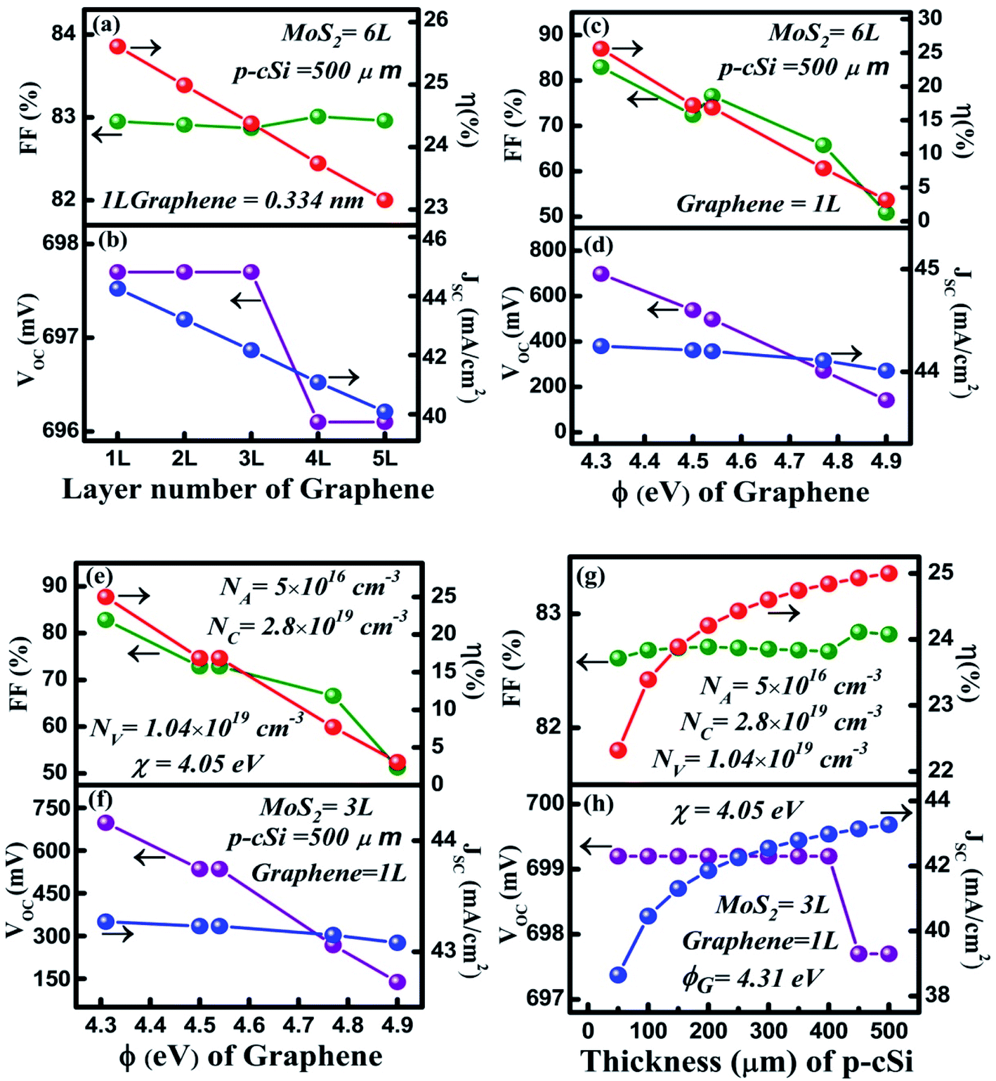 | ||
| Fig. 5 Optimization of the graphene (front contact) layer: (a) and (b) optimization of the graphene layer number, (c) and (d) optimization of the Φ (eV) of the graphene layer in which the parameters of n-MoS2 and p-cSi are maintained at their best-optimized values, (e) and (f) optimization of the Φ (eV) of the graphene layer and (g) and (h) optimization of the thickness of a commercially available silicon wafer with practically available p-cSi parameters. | ||
The presence of a strong covalent bond between the C and Mo atoms or the presence of a dangling bond of sulfur present in the interfaces affects the interfacial barrier height and a variation in the barrier height results in a variation in the contact resistance.60,61 Usually, the contact resistance is a vital factor that affects the solar cell performance.62 However, many experimental reports suggest that by controlling the Fermi level (i.e. the work function) of graphene, the contact resistance can be minimized in the graphene/MoS2 interfaces.63,64 Therefore, in this work, we have focused primarily on the work function of graphene. The depicted results shown in Fig. 5c and d, show the variation of the cell parameters with the variation of the graphene work function (ΦGr) from 4.31 to 4.9 eV. A large reduction in the VOC was observed in Fig. 5d, in which it decreased from 697.7 to 141.4 mV with an increase of ΦGr. From eqn (2), it can be observed that with the increase in ΦGr, the potential barrier energy eVbi of graphene/n-MoS2 decreases. It has also been reported that when the ΦTCO (contact) of Si HIT solar is low, the eVbi of the TCO (transparent conducting oxide)/n-type emitter has the same direction as that of the eVbi of the n-emitter/p-Si. On the other hand, when the ΦTCO (contact) is high, the eVbi of the TCO/n-type emitter contact will have an inverted direction to that of the eVbi of the n-emitter/p-Si junction. Moreover, with the increase in the Φ of the TCO contact in the silicon HIT solar cell, the depletion region in the emitter region increases and widens and results in the overlap of the contact/n-type emitter region and the n-type emitter/p-type silicon junction region if the emitter is not sufficiently thin enough.4 Thus, the higher ΦGr might increase the possibility of overlapping between the graphene/n-MoS2 depletion region and the n-MoS2/p-cSi depletion region, which has resulted in a reduction in the VOC. In contrast, owing to the overlap of the graphene/n-MoS2 depletion region and the n-MoS2/p-cSi depletion region, the eVbi of n-MoS2/p-cSi reduces. This results in a reduction of the built-in electric field which is unable to push the photo-generated carriers effectively to their respective sides under short circuit conditions and thus the JSC is observed to decline linearly from 44.25 to 40.09 mA cm−2 with an increase in the ΦGr. The overall reduction in the VOC and JSC reduced η from 25.61% to 23.15%. The maximum η = 25.61% was achieved at ΦGr = 4.31 eV of pristine graphene.
To validate our simulated results, a comparison has been performed by considering the best-optimized values of n-MoS2 and a-Si:H(i) with the practically available p-cSi parameters by varying the ΦGr and p-cSi thickness within the range of 4.31–4.9 eV and the 50–500 μm range respectively, as depicted in Fig. 5e–h and Table 4, using the practically available data for p-cSi.52,65 It can be seen from Fig. 5e and f, that the maximum η = 25% was obtained at ΦGr = 4.31 eV, which is close to our best-optimized results as shown in Fig. 5c and d. Similarly, in Fig. 5g and h, the same maximum η = 25% was achieved for a 500 μm thick p-cSi wafer.
| Cell parameter | Most optimized cell (before optimization of the parameters of the graphene layers) | Graphene layer number optimized cell (after optimization of n-MoS2 and p-cSi) | n-cSi wafer optimized cell for practically available silicon parameters |
|---|---|---|---|
| V OC (mV) | 696.1 | 697.7 | 697.7 |
| J SC (mA cm−2) | 40.09 | 44.25 | 43.27 |
| FF (%) | 82.96 | 82.95 | 82.82 |
| η (%) | 23.15 [@ 3L n-MoS2 at ND = 1018 cm−3, NC/NV = 3 × 1020 cm−3, Eg = 1.47 eV, χ = 4.47 eV, εr = 6, μn = 517 cm2 V−1 s−1, μp = 8.5 cm2 V−1 s−1, and @ 6 nm a-Si:H(i) at Eg = 1.6 eV and @ 500 μm p-cSi at NA = 1 × 1017 cm−3, NC/NV = 3 × 1019 cm−3, χ = 4.05 eV and @ 5L graphene at Φ = 4.31 eV] | 25.16 [@ 3L n-MoS2 at ND = 1018 cm−3, NC/NV = 3 × 1020 cm−3, Eg = 1.47 eV, χ = 4.47 eV, εr = 6, μn = 517 cm2 V−1 s−1, μp = 8.5 cm2 V−1 s−1, and @ 6 nm a-Si:H(i) at Eg = 1.6 eV and @ 500 μm p-cSi at NA = 1 × 1017 cm−3, NC/NV = 3 × 1019 cm−3, χ = 4.05 eV and @ 1L graphene at Φ = 4.31 eV] | 25 [@ 3L n-MoS2 at ND = 1018 cm−3, NC/NV = 3 × 1020 cm−3, Eg = 1.47 eV, χ = 4.47 eV, εr = 6, μn = 517 cm2 V−1 s−1, μp = 8.5 cm2 V−1 s−1, and @ 6 nm a-Si:H(i) at Eg = 1.6 eV and @ 500 μm p-cSi at NA = 5 × 1016 cm−3, NC/NV = 2.8 × 10¹⁹/1.04 × 1019 cm−3, χ = 4.05 eV and @ 1L graphene at Φ = 4.31 eV] |
3.5 Variation and simulation of the front contact and back contact material
In this section, a comparison of the cell parameters has been performed by changing the front contact material graphene to ITO and Al19 and the back contact to Ag. As seen in Fig. 6a and b the thickness of ITO is considered to be 80 nm and the ΦITO has been varied from 4.40–4.50 eV.34 The maximum values for VOC, JSC, FF and η were obtained and found to be 625.8 mV, 31.47 mA cm−2, 80.41% and 15.33% respectively. Similarly, in Fig. 6c and d, when ΦAl was varied, the maximum values for VOC, JSC, FF, and η were found to be 650.8 mV, 4.36 mA cm−2, 82.79% and 2.353%, respectively. In both cases, η was significantly lower than that of η obtained using the graphene layer as a contact. | ||
| Fig. 6 Changing the front and back contact: (a) and (b) variation in the Φ (eV) of ITO, (c) and (d) variation in the Φ (eV) of Al, and (e) and (f) variation in the Φ (eV) of Ag. | ||
Fig. 6e and f shows the variation in the cell parameters when the back contact was changed from Au to Ag and the Φ of Ag was maintained from 4.64 to 4.74 eV. It was observed that in this range of Φ for Ag, the VOC increased from 664.8 to 677.3 mV, whereas the JSC remained constant at 42.76 mA cm−2. The FF and η were observed to decrease from 82.72% to 83.5% and 23.51% to 24.19%, respectively. This η was close to our simulated ηmax value, that is, 25.61% when we used Au as a contact. Here, the back contacts have been considered as the uniform thin film deposited on the backside of p-cSi.
3.6 maximum power and series resistance
The proposed solar cell as shown in Fig. 1a was simulated and characterized under a standard AM1.5G spectrum and forward voltage in the range of 0 to 0.7 V. The IV characteristics of the best optimized solar cell generated by the software are shown in Fig. 7. The maximum power delivered by the cell, as well as the series resistance (Rs), was calculated from the IV characteristics and found to be 25.4 mW cm−2 and 2.5 Ω cm2 was achieved respectively (see ESI†).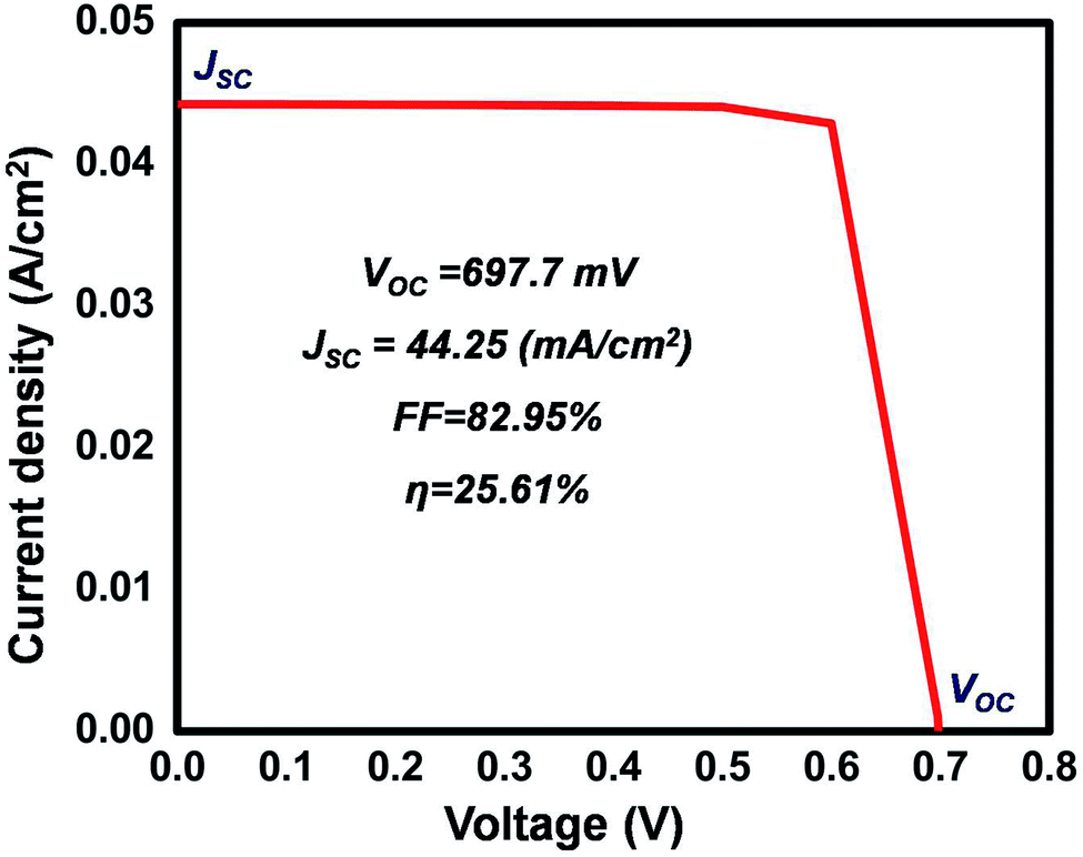 | ||
| Fig. 7 IV characteristics of the most optimized cell. | ||
Finally, a comparison between the experimental and theoretical demonstration of graphene, MoS2, and Si-based solar cells was performed and the results are detailed in Table 5. However, except for our work none of the studies used graphene as a contact material or TCE.
| Type of study | Solar cell structure | V OC (V) | J SC (mA cm−2) | FF (%) | η (%) | Ref. |
|---|---|---|---|---|---|---|
| Experimental | ITO/graphene/MoS2/n-cSi/(Ti/Ag) | 0.59 | 36.8 | 73 | 15.8 | 66 |
| Experimental | Au/graphene/MoS2/n-Si/In | 0.56 | 33.4 | 60 | 11.1 | 67 |
| Experimental | Au/graphene/MoS2/n-Si/Au | 0.50 | 28.1 | 47 | 6.56 | 68 |
| Experimental | Pd/n-MoS2/i-SiO2/p-Si/In | 0.30 | 5.5 | 42 | 4.5 | 69 |
| Experimental | Ni/graphene/MoS2/p-csi/Al | 0.51 | — | — | 2.58 | 70 |
| Theoretical | TCO/MoS2/SiGe:H/p-Si/Al | 0.652 | 40.01 | 83.7 | 21.85 | 3 |
| Theoretical | Graphene/n-MoS2/a-Si:H/p-cSi/Au | 0.697 | 44.25 | 82.95 | 25.61 | This work |
4. Conclusions
In order to develop an efficient HIT solar cell, a graphene/n-MoS2/a-Si:H(i)/p-cSi/Au structure has been proposed and simulated using AFORS-HET v 2.5 software. The individual effects of the six parameters of the n-MoS2 layer were analyzed individually. After optimizing the parameters of the n-MoS2, a-Si:H(i), and p-cSi layers, an optimum efficiency of 23.15% was achieved. As the contact material in a solar cell has an adverse effect on the cell performance, a further simulation was performed to observe the effect of graphene on the proposed HIT solar cell by varying the number of layers and the work function. From this simulation, a maximum efficiency of 25.61% was achieved for single-layer graphene at a work function of 4.1 eV. On the other hand, by changing the front contact graphene to ITO and Al we achieved efficiencies of 15.33% and 2.35%. This confirms that graphene could be an efficient contact material for use in an n-MoS2/a-Si:H(i)/p-cSi/Au HIT solar cell. Our simulated results establish that the graphene layer could be an effective contact TCE material and n-MoS2 could be an efficient emitter layer in a single facial n-MoS2 and p-cSi based HIT solar cell.Conflicts of interest
There are no conflicts to declare.Acknowledgements
The authors are very thankful to Helmholtz-Zentrum Berlin for providing us with the AFORS-HET simulation software and the Department of Science and Technology (DST), Ministry of India for their financial support.References
- N. Dwivedi, S. Kumar, A. Bisht, K. Patel and S. Sudhakar, Sol. Energy, 2013, 88, 31–41 CrossRef CAS.
- M. Belarbi, M. Beghdad and A. Mekemeche, Sol. Energy, 2016, 127, 206–215 CrossRef CAS.
- S. Xu, X. Zeng, W. Wang, G. Zhou, Y. Hu and S. Wu, J. Miner. Mater. Char. Eng., 2017, 5, 323–338 CAS.
- L. Zhao, C. L. Zhou, H. L. Li, H. W. Diao and W. J. Wang, Sol. Energy Mater. Sol. Cells, 2008, 92, 673–681 CrossRef CAS.
- K. Masuko, M. Shigematsu, T. Hashiguchi, D. Fujishima, M. Kai and N. Yoshimura, IEEE J. Photovolt., 2014, 4, 1433–1435 Search PubMed.
- I. Khrapach, F. Withes, T. H. Bointon, D. K. Polyushkin, W. L. Barnes, S. Russo and M. F. Craciun, Adv. Mater., 2012, 24, 2488–2849 CrossRef PubMed.
- P. Lazar, R. Zboril, M. Pumera and M. Otyepka, Phys. Chem. Chem. Phys., 2014, 16, 14231–14235 RSC.
- J. H. Kim, J. H. Hwang, J. Suh, S. Tongay, S. Kwon, C. C. Hwang, J. Wu and J. Y. Park, Appl. Phys. Lett., 2013, 103, 171604 CrossRef.
- A. S. Mayorov, R. V. Gorbachev, S. V. Morozov, L. Britnell, R. Jalil, L. A. Ponomarenko, P. Blake, K. S. Novoselov, K. Watanbe, T. Taniguchi and A. K. Geim, Nano Lett., 2011, 11, 2396–2399 CrossRef CAS PubMed.
- X. Zhong, W. Zhou, Y. Peng, Y. Zhou, F. Zhou, Y. Yin and D. Tang, RSC Adv., 2015, 5, 45239 RSC.
- B. Radisavljevic, A. Radenovic, J. Brivio, V. Giacometti and A. Kis, Nat. Nanotechnol., 2011, 6, 147 CrossRef CAS PubMed.
- B. Radisavljevic and A. Kis, Nat. Mater., 2013, 12, 815 CrossRef CAS PubMed.
- D. S. Tsai, K. K. Liu, D. H. Lien, M. L. Tsai, C. F. Kang and C. A. Lin, ACS Nano, 2013, 7, 3095–3911 CrossRef PubMed.
- X. Yang, W. Fu, W. Liu, J. Hong, Y. Cai, C. Jin, M. Xu, H. Wang, D. Yang and H. Chen, J. Mater. Chem. A, 2014, 2, 7727 RSC.
- J. M. Yun, Y. J. Noh, J. S. Yeo, Y. J. Go, S. I. Na, H. G. Jeong, J. Kim, S. Lee, S. S. Kim, H. Y. Kim and D. Y. Kim, J. Mater. Chem. C, 2013, 1, 3777 RSC.
- S. Choi, Z. Shaolin and W. Yang, J. Korean Phys. Soc., 2014, 64, 1550–1555 CrossRef CAS.
- J. H. Li, D. Lee, D. Qu, X. Liu, J. Ryu and A. Seabaugh, Nat. Commun., 2015, 6, 6564 CrossRef PubMed.
- Y. Du, H. Liu, A. T. Neal, M. Si and P. D. Ye, IEEE Electron Device Lett., 2013, 34, 1328–1330 CAS.
- M. L. Tsai, S. H. Su, J. K. Chang, D. S. Tsai, C. H. Chen and C. I. Wu, ACS Nano, 2014, 8, 8317–8322 CrossRef CAS PubMed.
- L. Hao, Y. Liu, W. Gao, Z. Han, Q. Xue and H. Zeng, J. Appl. Phys., 2015, 117, 114502 CrossRef.
- D. D. Tune, N. Mallik, H. Fornasier and B. S. Flavel, Adv. Energy Mater., 2020, 10, 1903261 CrossRef CAS.
- M. Bat-Erdene, M. Batmunkh, S. A. Tawfik, M. Fronzi, M. J. Ford, C. J. Shearer, L. Yu, M. Dadkhah, J. R. Gascooke, C. T. Gibson and J. G. Shapter, Adv. Funct. Mater., 2017, 1704488 CrossRef.
- L. Yu, A. S. R. Bati, T. S. L. Grace, M. Batmunkh and J. G. Shapter, Adv. Energy Mater., 2019, 1901063 CrossRef.
- S. Lin, P. Wang, X. Li, Z. Wu, Z. Xu and S. Zhang, Appl. Phys. Lett., 2015, 107, 153904 CrossRef.
- Z. Qiao, J. L. Ji and Y. L. Zhang, Chin. Phys. B, 2017, 26, 068802 CrossRef.
- L. Fan, F. Wang, J. Liang, X. Yao, J. Fang and D. Zhang, J. Semicond., 2017, 38, 014003 CrossRef.
- H. Keum, H. J. Chung and S. Kim, ACS Appl. Mater. Interfaces, 2013, 5, 6061–6065 CrossRef CAS PubMed.
- Introduction to Quantum Transport in Low-Dimensional Systems, http://www.hri.res.in/%7Enanotr16/notes/KJThomas-1.pdf, accessed July 2018 Search PubMed.
- S. D. Sarma, S. Adam, E. H. Hwang and E. Rossi, Rev. Mod. Phys., 2011, 83, 407 CrossRef.
- J. Suh, T. E. Park, D. Y. Lin, D. Fu, J. Park and H. J. Jung, Nano Lett., 2014, 14, 6976–6982 CrossRef CAS PubMed.
- Z. Lin, B. R. Carvalho, E. Kahn, R. Lv and R. Rao, 2D Matter., 2016, 3, 022002 CrossRef.
- A. I. Pantazi and V. Yannopapas, Opt. Commun., 2016, 374, 24–28 CrossRef CAS.
- K. Patel and P. K. Tyagi, Carbon, 2017, 116, 744–752 CrossRef CAS.
- Y. Park, V. Choong, Y. Gao, B. R. Hsieh and C. W. Tang, Appl. Phys. Lett., 1996, 68, 2699–2701 CrossRef CAS.
- A. Kahn, Fermi level, work function and vacuum level, Mater. Horiz., 2016, 3, 7–10 RSC.
- R. M. Eastment and C. H. B. Mee, J. Phys. F: Met. Phys., 1973, 3, 1738–1745 CrossRef CAS.
- A. W. Dweydari and C. H. B. Mee, Phys. Status Solidi A, 1975, 27, 223–230 CrossRef CAS.
- Z. H. Ni, H. M. Wang, J. Kasim, H. M. Fan, T. Yu and Y. H. Wu, Nano Lett., 2007, 7, 2758–2763 CrossRef CAS PubMed.
- F. J. Nelson, V. K. Kamineni, T. Zhang, E. S. Comfort, J. U. Lee and A. C. Diebold, Appl. Phys. Lett., 2010, 97, 253110 CrossRef.
- C. P. Lu, G. Li, J. Mao, L. M. Wang and E. Y. Andrei, Nano Lett., 2014, 14, 4628 CrossRef CAS PubMed.
- B. Radisavljevic and A. Kis, Nat. Mater., 2013, 12, 815–820 CrossRef CAS PubMed.
- K. F. Mak, C. Lee, J. Hone, J. Shan and T. Y. Heinz, Phys. Rev. Lett., 2010, 105, 136805 CrossRef PubMed.
- E. J. G. Santos and E. Kaxiras, ACS Nano, 2013, 7, 10741–10746 CrossRef CAS PubMed.
- S. L. Howell, D. Jariwala, C. C. Wu, K. S. Chen, V. K. Sangwan and J. Kang, Nano Lett., 2015, 15, 2278–2284 CrossRef CAS PubMed.
- O. Salehzadesh, N. H. Tran, X. Liu, I. Shihand and Z. Mi, Nano Lett., 2014, 14, 125–4130 Search PubMed.
- H. Zhang, Y. Ma, Y. Wan, X. Rong, Z. Xie and W. Wang, Sci. Rep., 2015, 5, 8440 CrossRef CAS PubMed.
- W. Zhou, X. Zou, S. Naijmaei, Z. Liu, Y. Shi and J. Kong, Nano Lett., 2013, 13, 2615–2622 CrossRef CAS PubMed.
- X. Garros, G. Reimbold, J. Cluzel, D. Muñoz and P.-J. Ribeyron, Microelectron. Eng., 2011, 88, 1247–1250 CrossRef CAS.
- L. Qin, Y. Xiao-Jun, L. Cheng and C. Ming-bo, Optoelectron. Lett., 2010, 6, 0108–0111 CrossRef.
- W. Lisheng and C. Fengxiang, J. Optoelectron. Adv. Mater., 2011, 13, 81–88 Search PubMed.
- A. Rawat, M. Sharma, D. Chaudhary, S. Sudhakar and S. Kumar, Sol. Energy, 2014, 110, 691–703 CrossRef CAS.
- L. Zhao, H. L. Li, C. L. Zhou, H. W. Diao and W. J. Wang, Sol. Energy, 2009, 83, 812–816 CrossRef CAS.
- F. Rana, Semiconductor Heterostructure, in Semiconductor Optoelectronics, 2017, ch. 2, https://courses.cit.cornell.edu/ece533/Lectures/handout2.pdf Search PubMed.
- J. Singh, Semiconductor devices: Basic Principles, Wiley India (P) Ltd, New Delhi, 2004 Search PubMed.
- V. K. Thakur and M. K. Thakur, Chemical Functionalization of Carbon Nanomaterials: Chemistry and Applications, CRC Press, New York, 2016, p. 918 Search PubMed.
- A. V. Sachenko, V. P. Kostylyov, M. V. Gerasymenko, R. M. Korkishko, M. R. Kulish and M. I. Slipchenko, Quantum Electronics & Optoelectronics, 2016, 19, 67–74 Search PubMed.
- Y. Zhao, C. Liang, M. Sun, Q. Liu, F. Zhang and D. Li, J. Appl. Phys., 2014, 116, 154506 CrossRef.
- Y. Zhou and G. Long, J. Phys. Chem. C, 2017, 121, 1455–1462 CrossRef CAS.
- W. Lisheng, C. Fengxiang and A. Yu, J. Phys.: Conf. Ser., 2011, 276, 012177 CrossRef.
- N. Jensen, R. M. Hausne, R. B. Bergmann, J. H. Werner and U. Rau, Prog. Photovoltaics Res. Appl., 2002, 10, 1–13 CrossRef CAS.
- X. Liu, J. Gao, G. Zhang and Y. W. Zhang, Nano Res., 2017, 10, 2944–2953 CrossRef CAS.
- M. Houssa, K. Iordanidou, A. Dabral, A. Lu, R. Meng, G. Pourtois, V. V. Afanas'ev and A. Stesmans, Appl. Phys. Lett., 2019, 114, 163101 CrossRef.
- D. K. Schroder and D. L. Meier, IEEE Trans. Electron Devices, 1984, 31(5), 637–647 Search PubMed.
- Y.-J. Yu, Y. Zhao, S. Ryu, L. E. Brus, K. S. Kim and P. Kim, Nano Lett., 2009, 9, 3430–3434 CrossRef CAS PubMed.
- H. Wang, L. Yu, Y.-H. Lee, Y. Shi, A. Hsu, M. L. Chin, L.-J. Li, M. Dubey, J. Kong and T. Palacios, Nano Lett., 2012, 12, 4674–4680 CrossRef CAS PubMed.
- J. Ma, H. Bai, W. Zhao, Y. Yuan and K. Zhang, Sol. Energy, 2018, 160, 76–84 CrossRef CAS.
- Y. Tsuboi, F. Wang, D. Kozawa, K. Funahashi, S. Mouri, Y. Miyauchi, T. Takenobub and K. Matsuda, Nanoscale, 2015, 7, 14476–14482 RSC.
- K. Jiao, C. Duan, X. Wu, J. Chen, Y. Wang and Y. Chen, Phys. Chem. Chem. Phys., 2015, 17, 8182 RSC.
- L. Z. Hao, W. Gao, Y. J. Liu, Z. D. Han, Q. Z. Xue, W. Y. Guo, J. Zhu and Y. R. Li, Nanoscale, 2015, 7, 8304–8308 RSC.
- W. Shi and M. Xiying, Coatings, 2018, 8, 2 Search PubMed.
Footnote |
| † Electronic supplementary information (ESI) available. See DOI: 10.1039/d0na00309c |
| This journal is © The Royal Society of Chemistry 2020 |