
Patterning technologies of quantum dots for color-conversion micro-LED display applications
Yuhui
Wang†
a,
Yunshu
Luo†
a,
Xuemin
Kong
a,
Tingzhu
Wu
 a,
Yue
Lin
*ab,
Zhong
Chen
*ab and
Shuli
Wang
*a
a,
Yue
Lin
*ab,
Zhong
Chen
*ab and
Shuli
Wang
*a
aFujian Engineering Research Center for Solid-State Lighting, Department of Electronic Science, School of Electronic Science and Engineering, Xiamen University, Xiamen, 361102 Fujian, China. E-mail: yue.lin@xmu.edu.cn; chenz@xmu.edu.cn; slwang@xmu.edu.cn
bInnovation Laboratory for Sciences and Technologies of Energy Materials of Fujian Province (IKKEM), Xiamen, 361102 Fujian, China
First published on 4th December 2024
Abstract
Quantum dot (QD) materials and their patterning technologies play a pivotal role in the full colorization of next-generation Micro-LED display technology. This article reviews the latest development in QD materials, including II–VI group, III–V group, and perovskite QDs, along with the state of the art in optimizing QD performance through techniques such as ligand engineering, surface coating, and core–shell structure construction. Additionally, it comprehensively covers the progress in QD patterning methods, such as inkjet printing, photolithography, electrophoretic deposition, transfer printing, microfluidics, and micropore filling method, and emphasizes their crucial role in achieving high precision, density, and uniformity in QD deposition. This review delineates the impact of these technologies on the luminance of QD color-conversion layers and devices, providing a detailed understanding of their application in enhancing Micro-LED display technology. Finally, it explores future research directions, offering valuable insights and references for the continued innovation of full-color Micro-LED displays, thereby providing a comprehensive overview of the potential and scope of QD materials and patterning technologies in this field.
 Yuhui Wang | Yuhui Wang received his Bachelor of Engineering degree from Xiamen University in 2022. He is currently pursuing his Master of Engineering degree at the Department of Electronic Science, School of Electronic Science and Engineering, Xiamen University, under the direction of Professor Zhong Chen. His current research interest focuses on microfluidics-based patterning of quantum dots for color conversion full-color micro-LED displays. |
 Yunshu Luo | Yunshu Luo received her Bachelor of Engineering degree from the School of Electronic Science and Engineering, Xiamen University, in 2023. Now, she is a graduate student at Xiamen University, under the guidance of Professor Wang Shuli. Her research interests include inkjet printing of perovskite nanocrystal color-conversion layers for full-color micro-LED display technology. |
 Yue Lin | Yue Lin is an associate professor in the Department of Electronic Science, Xiamen University. His research scope includes (a) micro-LED display technology, (b) electrohydrodynamic inkjet printing for quantum dot color conversion layers, (c) GaN- and AlGaN-based semiconductor materials and devices and optoelectronic properties, and (d) all-inorganic and hybrid perovskite quantum dots and the optoelectronic properties. As the first and/or corresponding author, he has published more than 30 papers in journals such as Advanced Materials, Advanced Optical Materials, Small, Journal of Materials Chemistry C, Photonics Research, and Applied Physics Letters. He has hosted fundings including NSF of China, NSF and Cooperation of Fujian Province. |
 Zhong Chen | Chen Zhong received his Ph.D. from Xiamen University, China, in 1993. Currently, he is Professor and Dean of the School of Electronic Science and Engineering at Xiamen University and Executive Director of the National Innovation Platform for the Fusion of Industry and Education in Integrated Circuits at Xiamen University. His research interests mainly focus on LED lighting and display, magnetic resonance and medical imaging. To date, he has published more than 570 SCI papers in journals such as Nature Communications, Advanced Materials, Journal of the American Chemical Society, and Angewandte Chemie International Edition. |
 Shuli Wang | Shuli Wang received his B.S. degree in June 2013 and his Ph.D. in June 2018 from Jilin University, under the supervision of Professor Junhu Zhang. He then conducted postdoctoral research in Professor Xu Hou's group at Xiamen University from September 2018 to February 2022. In March 2022, he joined the School of Electronic Science and Engineering at Xiamen University as Assistant Professor. His current research interests include perovskite nanocrystals, patterning technology, Micro-LED displays, and bioinspired materials. He has published over 50 papers in journals such as Nature, Science Advances, Advanced Materials, Accounts of Materials Research, Nano Letters, and Small. |
1. Introduction
Displays, one of the ideal interfaces for human–machine interaction, provide clear and accurate images and text, enabling efficient and intuitive interaction with computers.1–3 High-resolution displays reveal more details, enhancing image realism and fidelity, which, in turn, improves user satisfaction with graphical interfaces and overall usability. With the rise of the “metaverse” concept, there has been growing interest in both academia and industry towards near-eye displays, particularly those suitable for virtual reality (VR), augmented reality (AR), and mixed reality.2,4,5 These application domains demand higher optical quality, resolution, color vividness, and contrast from modern displays.6 To meet these demands, the development of new display technologies with high resolution and image quality is crucial for optimizing visual experience.7 Micro-LED display technology, which constructs self-emissive pixel units using Micro-LED chips smaller than 50 μm and assembles these pixels into high-density arrays, is regarded as the “ultimate display technology” in the realm of flat-panel displays.8,9 Owing to its outstanding performance in terms of brightness, contrast, viewing angles, energy consumption, response speed, resolution, lifespan, and color rendering, Micro-LED display technology shows promising applications in AR/VR, optical communication/optical interconnects, flexible transparent displays, and smart car lighting.10–12 Consequently, Micro-LED display technology has become a hot research topic in the fields of optoelectronic materials and display technologies in recent years.To achieve superior visual experience, the construction of full-color Micro-LED displays requires the formation of micro-scale RGB pixel points. The realization of Micro-LED full-color displays mainly relies on two approaches: a three-primary-color chip scheme and color-conversion scheme.13,14 The three-primary-color chip scheme achieves full color by integrating arrays of RGB three-primary-color Micro-LED chips onto the display backplane.13–16 This scheme depends on high-precision massive transfer technology but suffers from lower transfer precision, lower product yield, and higher difficulty in repair, leading to higher costs for Micro-LED display products.15 Additionally, voltage differences between Micro-LEDs of different colors increase the complexity of the driver circuit design. By contrast, the color-conversion scheme uses fluorescent materials to emit fluorescence under the excitation of blue or UV Micro-LED chips to achieve full color.4,17,18 Currently, the fabrication technology of blue Micro-LED chips is relatively mature and can realize full-color display by exciting fluorescent materials that emit red and green colors. Although this approach is simple and straightforward, it needs to address the issue of blue light leakage to avoid reducing the color purity and gamut of the display and to protect against potential harm to humans. In comparison, the color-conversion scheme for full colorization using UV Micro-LED chips requires the combination of RGB fluorescent materials. Generally, fluorescent materials exhibit good absorption properties for UV light, and technology for addressing the issue of UV light leakage is also relatively mature.
In color-conversion schemes, fluorescent materials must possess the following characteristics to ensure the color purity and color gamut of Micro-LED display devices: small size, high luminous intensity, narrow full width at half maximum (FWHM), and high quantum yields.5,19 Traditional phosphors such as calcium halophosphate phosphors and rare-earth trichromatic phosphors are not suitable for fabricating uniformly emitting micro-scale pixel points due to their larger particle sizes and slow response.13,17 In contrast, nanometer-scale quantum dot (QD) materials are ideal for achieving full-color Micro-LED displays via color conversion.5,20,21 QDs are semiconductor nanocrystals with quantum confinement effects, and their characteristic size is typically no larger than twice the Bohr radius of the exciton in the corresponding semiconductor material.22 QDs exhibit unique properties such as narrow emission spectra, high quantum yield, and tunable bandgaps, and they can emit light across a broad spectrum from visible to near-infrared.23 Currently, the QD materials used in full-color Micro-LED displays primarily include II–VI group QDs, III–V group QDs, and perovskite QDs. However, the photoluminescence (PL) performance of QD materials may degrade under complex conditions such as exposure to light, heat, water, and oxygen. To make QD materials more suitable for color conversion in Micro-LED displays, performance optimization is often required. These optimization measures include ligand engineering, coating techniques, and the fabrication of core–shell structures to enhance the luminous intensity and stability of QDs, thereby improving the stability and longevity of micro-display devices. Additionally, QD materials should have high ultraviolet or blue light absorption coefficients to increase the light conversion efficiency.
In addition to high-quality QD materials, developing reliable QD patterning technologies is crucial for achieving high precision, high density, and high uniformity in QD deposition on target substrates. The patterning technology significantly impacts the resolution and luminous performance of Micro-LED full-color display devices. Currently, researchers have developed various QD patterning methods including inkjet printing,24–29 photolithography,30–33 electrophoretic deposition,34,35 microfluidic techniques,36–38 micro-transfer printing,39 and micropore filling method.40–42 Each method has its own advantages and limitations. From the perspective of QD color conversion for Micro-LED displays, an ideal patterning technology should not only produce uniform and high-resolution pixel patterns but also be capable of creating QD films with the required thickness to efficiently absorb background blue or UV light. This enhancement in light conversion efficiency reduces background light leakage and improves color purity. According to Beer-Lambert's law, the optical absorbance of QD films is related to the QD absorption coefficient, film thickness, and QD concentration (including solid content and porosity). Given that QDs typically have high absorption coefficients, with molar extinction coefficients generally in the range of 105–106 M−1 cm−1, achieving 99.9% UV or blue light absorption would require a QD film thickness of at least several micrometers, assuming the film is composed of pure QDs.43–45 QD patterning techniques involve specific process conditions that may affect the performance of the QDs during patterning, thereby influencing the overall performance and stability of Micro-LED display devices. Therefore, an ideal QD patterning technology should minimize damage to the QDs to maintain the optimal performance of the prepared display devices.
In this review, we will comprehensively explore the latest advancements in QD materials and their patterning technologies for full-color Micro-LED displays (Fig. 1). First, we will provide an in-depth introduction to the commonly used QD materials in Micro-LED color-conversion full-color schemes including II–VI group QDs, III–V group QDs, and emerging perovskite QDs. We will also discuss various methods for optimizing QD performance such as ligand engineering, coating technologies, and core–shell structure fabrication. Next, we will systematically elaborate on the latest research findings in QD patterning technologies including inkjet printing, photolithography, electrophoretic deposition, microfluidic techniques, transfer printing, and micropore filling method. Our focus will be on how these techniques achieve high precision, high density, and high uniformity in QD deposition on target substrates, and we will delve into the luminous performance of QD color-conversion layers and devices fabricated using these technologies. Finally, based on a comprehensive summary of recent developments in this field, we will look ahead to future research directions, aiming to provide valuable references and insights for the further development and innovation of full-color Micro-LED display technology.
 | ||
| Fig. 1 Commonly utilized QDs (inner cycle) and their pattering technologies (outer cycle) for constructing micrometer-scale color conversion pixel arrays for Micro-LED displays. Reprinted with permission from ref. 18, 56, 24 and 34. Copyright 2020, 2019, 2024, 2024, American Chemical Society. Reprinted with permission from ref. 30 and 80. Copyright 2022, 2022, Springer Nature. Reprinted with permission from ref. 29. Copyright 2020, John Wiley and Sons. Reprinted with permission from ref. 37, 38 and 40. Copyright 2023, 2023, 2022, Royal Society of Chemistry. | ||
2. Quantum dots for color-conversion micro-LED displays
2.1. II–VI group quantum dots
Traditional II–VI group semiconductor QDs such as CdS, ZnS, CdSe, ZnO, and CdTe (Fig. 2A)46 have found extensive applications in the optoelectronic field. The bandgap of II–VI group QDs can be precisely tuned through surface modification, size control, alloying, and ion doping, allowing their fluorescence emission wavelength to cover the entire visible spectrum. Fig. 2B presents the PL images and spectra of CdSe/CdS core–shell QDs with different emission wavelengths under UV excitation.47Fig. 2C displays the HRTEM image of CdSe/CdS/ZnS QDs.48 Significant progress has been made in the synthesis and performance optimization of CdSe QDs. Leading international companies such as QD Vision, Nanosys, Nanoco, and Poly OptoElectronics Co. Ltd have achieved large-scale production of CdSe-based QDs, which are widely used in the backlight design for liquid crystal displays. Additionally, electroluminescent QLED display technology based on CdSe QDs is also rapidly advancing. With the rise of Micro-LED display technology, CdSe QDs, one of the most mature QD materials, are emerging as key luminescent materials for color-conversion full-color Micro-LED displays. | ||
| Fig. 2 (A) Schematic of II–VI group QDs. Reprinted with permission from ref. 45. Copyright 2016, Baqiyatallah University of Medical Sciences. (B) PL images and spectra of CdSe/CdS core–shell QDs with different emission wavelengths. Reprinted with permission from ref. 46. Copyright 2012, American Chemical Society. (C) HRTEM image of CdSe/CdS/ZnS QDs. Reprinted with permission from ref. 47. Copyright 2022, Multidisciplinary Digital Publishing Institute. (D) Ligand passivation on the (100) facet with and without chloride ions. (E) HRTEM image of cubic CdSe QDs and SAED images. Reprinted with permission from ref. 54. Copyright 2020, American Chemical Society. (F) Schematic of a two-step epitaxial growth method for synthesizing CdSe/nZnSe QDs. (G) TEM image of the prepared CdSe/7ZnSe QDs. (H) Relationship between the PLQY and the thickness of ZnSe shells. Reprinted with permission from ref. 55. Copyright 2023, American Chemical Society. | ||
The synthesis of QDs involves nucleation and growth, which significantly influence the size, shape, structure, and properties of QDs. Murray et al. developed monodispersed CdSe, CdS, and CdTe QDs using high-temperature thermal injection at 300 °C, employing trioctylphosphine oxide (TOPO) as the solvent and trioctylphosphine (TOP) as the ligand.49 This method allowed separate nucleation and growth, maintaining a size distribution within 5% and precise control over grain size. Peng Xiaogang's group replaced TOPO with the non-coordinating solvent 1-octadecene (ODE) to synthesize CdS and CdSe QDs, providing a “green chemistry” synthetic route for quantum dots, which is conducive to achieving a safer and more environmentally friendly synthesis process.50,51
During the nucleation of QDs, the ligand significantly influences their growth dynamics. Ligand modification can reduce surface defects in QDs and improve the quantum yield, which is essential for efficient light-emitting devices. Talapin et al. added hexadecylamine (HDA) to the common trioctylphosphine/trioctylphosphine oxide (TOP/TOPO) system to accurately control CdSe QD growth. Surface passivation with inorganic (ZnS) or organic alkyl amine layers improved the quantum efficiency of CdSe QDs to 40–60%.52 Further improvements were achieved by using environmentally friendly cadmium acetate instead of dimethylcadmium, which led to an increase in the photoluminescence quantum yield (PLQY) of CdSe QDs to 85%.53
Coating a shell material on the core of QDs can effectively passivate the surface defects and reduce non-radiative recombination. Li et al. synthesized CdSe/CdS core–shell QDs using the successive ion layer adsorption and reaction (SILAR) technique.54 After applying five monolayers of CdS coating on the CdSe core, the size distribution remained consistent, with PLQY between 20% and 40% and FWHM between 23 and 26 nm, showing better optical properties and stability than bare CdSe nanocrystals. Lv et al. developed a two-step synthesis strategy with non-coordinating solvents, first creating small-sized CdSe QDs as seeds, then using chloride ligands to selectively grow cube-shaped dots with six (100) facets.55 These CdSe dots displayed monodisperse sizes and a quantum yield of about 90%, with a narrow FWHM of 20 nm. Fig. 2D compares ligand passivation on the (100) facet with and without chloride ions, showing that smaller chloride ions are more effective than alkylamide ligands for Cd sites. Fig. 2E shows the HRTEM images of cubic CdSe QDs with clear (200) and (220) planes and the selected area electron diffraction (SAED) images revealing clear square-symmetrical spots, confirming parallel lattice fringes and six equivalent (100) facets. Zhang et al. controlled the surface ligand strain and CdSe/ZnSe lattice strain using a two-step epitaxial growth method and synthesized green CdSe/ZnSe/ZnS core/shell/shell QDs with a nearly uniform PLQY (Fig. 2F).56 The TEM image in Fig. 2G shows the uniform size of the prepared QDs with 7 monolayers of the ZnSe shell. Fig. 2H shows the relationship between the PLQY of QDs and the ZnS and ZnSe shell thickness, and the maximum PLQY of 92% was achieved when the ZnSe shell thickness is 7 monolayers.
2.2. Perovskite quantum dots
Perovskite QDs have demonstrated significant potential in the display industry due to their exceptional PL intensity, narrow emission peak, and facility of synthesis. The structure of perovskite QDs is typically represented as ABX3 (Fig. 3A),57 where A denotes a monovalent organic cation such as methylammonium (CH3NH3+, MA+), formamidinium (CH(NH2)2+, FA+), phenylethylammonium (C6H5(CH2)2NH3+, PEA+), cesium (Cs+), or rubidium (Rb+); B represents a metal cation, such as lead (Pb2+), tin (Sn2+), zinc (Zn2+), or copper (Cu2+) ion; and X stands for a halide anion such as chloride (Cl−), bromide (Br−), or iodide (I−).58 Besides exploiting the quantum confinement effect by turning the size, directly shifting the intrinsic band-gap by changing the halide component ratio provides a more convenient way to adjusting the PL peak wavelength. By adjusting the halide composition, the emission wavelength of perovskite QDs can span the entire visible spectrum. Fig. 3B shows the PL images (top) and spectra (bottom) of perovskite QDs with different emission wavelengths under ultraviolet excitation.59Fig. 3C shows the typical TEM image of CsPbCl3, CsPbBr3, and CsPbI3 QDs, respectively.59–61 In practice, perovskite QDs are sensitive to external factors such as oxygen, moisture, temperature, and radiation, which can cause dissociation or phase transitions, resulting in non-emissive structures and affecting their optical performance and stability.58 Recent research has therefore aimed to enhance the stability and PLQY of perovskite QDs, employing strategies such as ion doping for lattice stabilization, ligand passivation to minimize surface defects, and coating with protective layers for surface preservation.62,63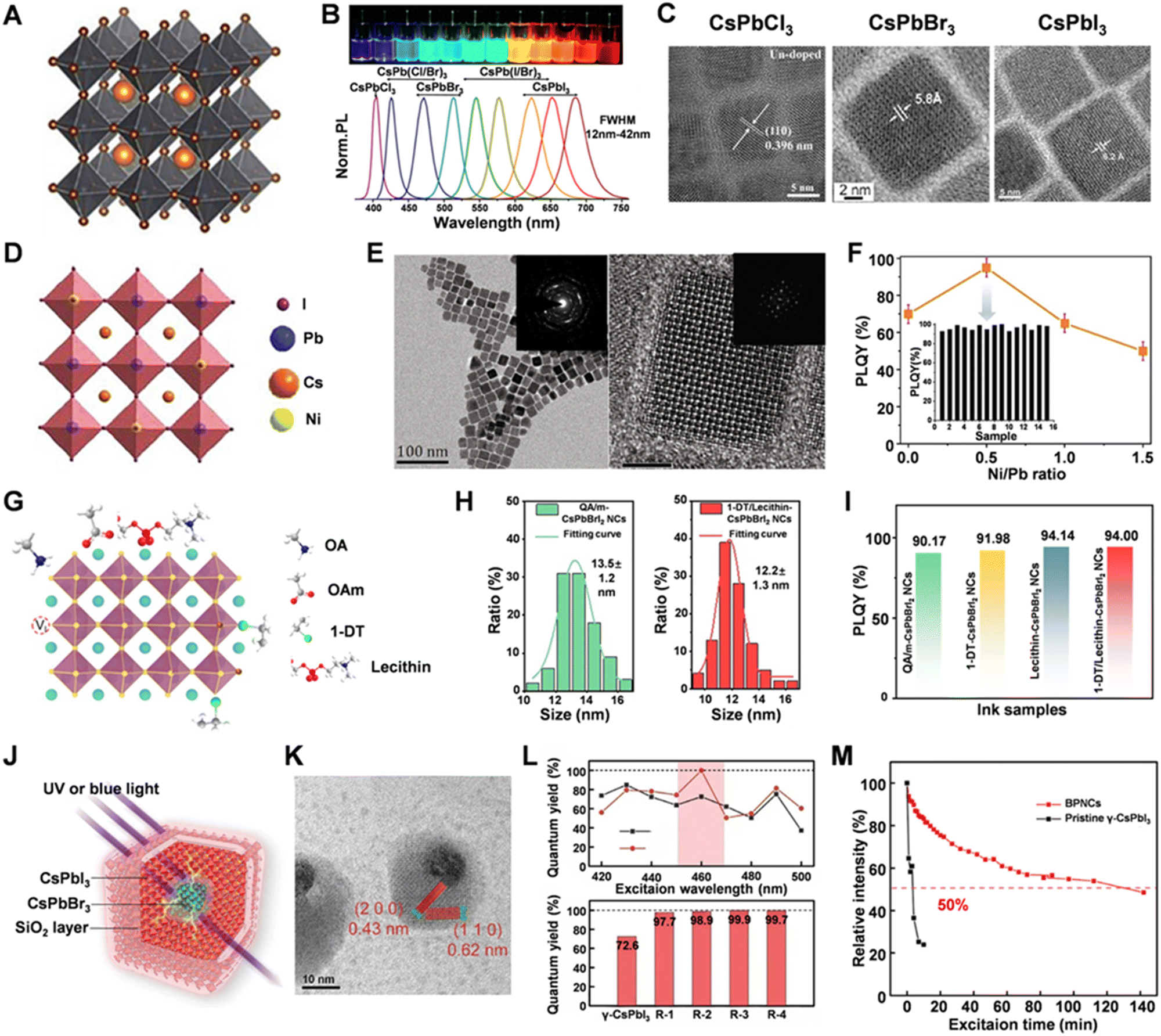 | ||
| Fig. 3 (A) Schematic of the structure of perovskite QDs. Reprinted with permission from ref. 56. Copyright 2019, American Chemical Society. (B) PL images and spectra of perovskite QDs with different emission wavelengths. Reprinted with permission from ref. 58. Copyright 2015, American Chemical Society. (C) HRTEM images of CsPbCl3, CsPbBr3, and CsPbI3 QDs. Reprinted with permission from ref. 58. Copyright 2015, American Chemical Society. Reprinted with permission from ref. 59. Copyright 2022, Elsevier. Reprinted with permission from ref. 60. Copyright 2019, John Wiley and Sons. (D) Schematic of the structure of Ni2+-doped CsPbI3 QDs. (E) TEM and HRTEM images of the Ni2+-doped CsPbI3 QD. (F) Relationship between the PLQY of the QDs and the Ni/Pb feed ratio. Reprinted with permission from ref. 63. Copyright 2021, Elsevier. (G) Schematic of dual-ligand (1-DT and lecithin)-stabilized CsPbBrI2 QDs. (H) Size distribution of the OA/OAm-passivated QDs and 1-DT/lecithin passivated CsPbBrI2 QDs. (I) PLQY of QDs stabilized by different ligands. Reprinted with permission from ref. 24. Copyright 2024, American Chemical Society. (J) Schematic illustration of the structure of core shell perovskite QDs with SiO2 protection layer. (K) TEM images of the core–shell perovskite QDs. (L) Quantum yield of QDs under different excitation lights, and different Br concentrations. (M) Comparison of the stability of the SiO2-passivated QDs compared to that without SiO2 protection. Reprinted with permission from ref. 41. Copyright 2023, John Wiley and Sons. | ||
By carefully selecting the ion types and concentrations, the optical, electrical, and stability properties of perovskite QDs can be optimized. Li et al. developed a Na+ ion doping method for CsPbBr3 QDs, which enhances oxidation and reduction tolerance by increasing the Br− vacancy diffusion barriers and reducing non-radiative recombination centers.64 Na+-doped green CsPbBr3 QDs show improved emission efficiency, color purity, PLQY, and stability against optical, thermal, and moisture effects. Liu et al. synthesized Ni2+-doped red CsPbI3 QDs by replacing Pb2+ with Ni2+, which increased lattice formation energy and improved structural stability, radiative lifetime, and environmental stability (Fig. 3D).65 TEM and HRTEM images (Fig. 3E) confirmed the cubic structure and lattice contraction of Ni2+-doped CsPbI3. Fig. 3F shows that the PLQY of the QDs can be increased to 95%–100% by adjusting the Ni/Pb feed ratio.
Mir et al. used zwitterionic lecithin as a capping ligand for CsPbI3, which, compared to traditional ligands OA and OAm, causes less surface strain and significantly enhances the stability.66 The modified CsPbI3 QDs remain stable in air for over 6 months. Yang et al. reported the passivation of CsPbBr3 QDs by dodecyl-dimethyl-ammonium bromide (DDAB)/PbBr2 and dispersed the QDs in non-polar solvent for preparing perovskite QD colloid inks with a PLQY of 94.06%.67 Xie et al. treated CsPbI3 QDs with hydrobromic acid and then replaced OA ligands with 1-dodecanethiol. This process reduced halide ion migration and increased the PLQY of the CsPbI3 QDs from 48% to 82%.68 Yang et al. proposed stabilizing strategy for dual ligands, 1-decanethiol (1-DT) and lecithin, to prepare mixed halide CsPbBrI2 QD (Fig. 3G) colloid ink specialized for EHD inkjet printing of high-resolution red pixels.24 The 1-DT and lecithin-passivated CsPbBrI2 QDs show a smaller size than that of control sample OA- and OAm-passivated QDs (Fig. 3H). The dual-ligand treatment QD ink not only shows the highest PLQY of 94% (Fig. 3I), but also possesses significantly improved stability. Li et al. replaced CsPbI3 long-chain ligands with 2-phenethylamine hydrochloride (TEAC), which reduced the defect density and achieved a PLQY of 92.5%.69 Li et al. used 2-naphthalenesulfonic acid (NSA) to suppress Ostwald ripening and ammonium hexafluorophosphate (NH4PF6) to replace long-chain ligands, achieving pure red CsPbI3 QDs with a quantum yield of 94% and maintaining over 80% quantum yield after 50 days.70
Huang et al. coated SiO2 shells on the perovskite QDs via a hydrolysis reaction of tetramethyl orthosilicate (TMOS). The synthesized CH3NH3PbBr3@SiO2 QDs showed a PLQY of 87% and maintained 94.10% of their initial luminescence after 7 hours of exposure to 470 nm blue light.71 Song et al. replaced the surface ligands of CsPbBr3 QDs with 3-aminopropyltriethoxysilane (APTES) and created a SiO2 shell via hydrolysis.72 These CsPbBr3@SiO2 QDs retained 35.8% of their luminescence after 48 hours in water, demonstrating excellent PL and water resistance. He et al. developed an in situ method to grow QDs within mesoporous silica nanospheres, resulting in silica-coated QDs with a PLQY of 87% and high stability.73 Fan et al. proposed dual-component core–shell QDs with silica coating (Fig. 3J).42 The QDs have red CsPbI3 QDs as the shell and green CsPbBr3 as the core. The TEM images in Fig. 3K show that CsPbI3 surrounds the CsPbBr3 core. The PL spectra show a luminescence peak of both bare γ-CsPbI3 and bicomponent QDs at 688 nm, while the intensity of the bicomponent QDs is significantly enhanced. The highest PLQY of red-emissive dual-component perovskite QD reached 99.9% (Fig. 3L). Under continuous blue LED excitation, the silica coated bicomponent samples showed apparently improved stability (Fig. 3M), demonstrating the great potential of the prepared QDs as color-conversion layers with blue micro-LED excitation.
2.3. III–V group quantum dots
Due to the toxicity of Cd-based QDs and Pb-containing perovskite QDs, low-toxicity III–V group QDs, particularly InP QDs, are emerging as eco-friendly alternatives. InP QDs exhibit a larger exciton Bohr radius and a direct bandgap, leading to notable quantum confinement and high stability. They are theoretically capable of covering the entire visible and near-infrared spectrum. Typically synthesized via the hot-injection method, InP QDs face challenges like surface defects and size uniformity despite their high PLQY and narrow FWHM. Enhancements in their performance can be achieved through improved synthesis, surface modifications, and core–shell design. Fig. 4A shows the schematic of the structure of InP/ZnSe/ZnS core/shell/shell QDs.74Fig. 4B displays the PL image (top) and spectrum (bottom) of InP QD emission across the visible range under UV excitation.75Fig. 4C presents the TEM images of blue InP/ZnS/ZnS, green InP/ZnSe/ZnS, and red InP/ZnSe/ZnS QDs. Compared to CdSe QDs, InP QDs have narrower spectral linewidths, making them ideal for high color purity displays. | ||
| Fig. 4 (A) Schematic of the structure of the InP/ZnSe/ZnS core/shell/shell QDs. Reprinted with permission from ref. 72. Copyright 2023, American Chemical Society. (B) PL image and spectrum of InP QDs emitting across the visible range. (C) TEM images of blue InP/ZnS/ZnS, green InP/ZnSe/ZnS, and red InP/ZnSe/ZnS QDs. Reprinted with permission from ref. 73. Copyright 2021, American Chemical Society. (D) Schematic of the synthesis flow of double-layer shell growth around InP cores. (E) TEM image and (F) PL spectrum of the prepared InP/ZnSe0.18S0.82/ZnS QDs. Reprinted with permission from ref. 74. Copyright 2020, American Chemical Society. (G) Schematic of Br− and I− passivated InP/ZnS/ZnS QDs. (H) TEM images of the InP/ZnS QDs and InP/ZnS/ZnS QDs. (I) PL and UV-visible absorption spectra of bromide-passivated blue InP QDs. Reprinted with permission from ref. 77. Copyright 2022, John Wiley and Sons. (J) Schematic of the QS strategy and TS strategy for synthesizing green InP/ZnSe/ZnS QDs. (K) TEM images and (L) absorption and PL spectra of QDs prepared using the two strategies. Reprinted with permission from ref. 78. Copyright 2022, Wiley-VCH Verlag. | ||
The synthesis methods for InP QDs primarily involve one-pot and two-step strategies, differing mainly in precursor types. The one-pot method uses a single precursor, while the two-step method employs two precursors to provide indium and phosphorus separately. Although simpler, the one-pot method lacks the compositional and size control of the two-step approach. Jo et al. utilized tri(dimethylamino)phosphine as a safer phosphorus source instead of the toxic trimethylsilane phosphine to create InP/ZnSexS1−x/ZnS green QDs via two-step synthesis.76Fig. 4D illustrates the synthesis flow, which involves a double-layer shell growth around InP cores. Initially, a ZnSexS1−x inner shell is formed with a compositional gradient, followed by a ZnS outer shell to enhance PL. As the ZnSe ratio in the inner shell increases, the QDs show improved uniformity. Fig. 4E displays the TEM image of InP/ZnSe0.18S0.82/ZnS QDs with an average diameter of about 9.1 nm. Fig. 4F presents the PL spectrum, showing a PL peak at 527 nm, an FWHM of 37 nm, and a PLQY of up to 87%. Kim et al. synthesized blue InGaP QDs via a cation exchange strategy, resulting in double-shell InGaP/ZnSeS/ZnS QDs with a blue shift from 475 to 465 nm and a high PLQY of 80–82%.77 Yu et al. synthesized InP-based QDs using sodium phosphide (NaOCP), achieving a tunable PL wavelength peak at 620 nm and a maximum PLQY of 97% by adjusting the precursor ratios and nucleation temperature.75
Ligands greatly enhance the PL of InP QDs by passivating surface defects. Common ligands for passivating InP QDs include halide ions, thiols (e.g., 1-octanethiol), phosphides, carboxylates, amines, and other organics. Calvin et al. employed metal halide salts (ZnCl2, ZnBr2, and InCl3) to facilitate ligand exchange on the surface of InP quantum dots, where more electronegative halogen ions replaced the less electronegative carboxylate ligands. This substitution reduced electron trapping caused by surface defects or miscoordinated environments, thereby enhancing the quantum yield, with ZnCl2 achieving a PLQY over 80%.78 Zhang et al. synthesized blue InP QDs using bromide passivation with low-temperature nucleation and high-temperature coating methods (Fig. 4G).79 The TEM images in Fig. 4H (left) show the InP core QDs with a ZnS shell, with a size of 3.8 ± 0.50 nm. Introducing 1-dodecanethiol (DDT) for a second ZnS shell resulted in InP/ZnS/ZnS QDs, with increased size of 6.2 ± 0.52 nm (Fig. 4H right). Fig. 4I displays the PL and UV-visible absorption spectra of these bromide-passivated blue InP QDs. The results indicate that the ZnBr2 passivation significantly improved the PLQY of the QDs from 54% to 93%.
Wu et al. introduced a quasi-shell growth strategy (QS strategy) for synthesizing green InP/ZnSe/ZnS QDs (Fig. 4J).80 In the traditional strategy (TS), Se precursors form a ZnSe shell at high temperatures, while in QS, Se precursors form a quasi-ZnSe (Q-ZnSe) shell at a lower temperature, which gradually transforms into ZnSe. Fig. 4K shows that the QS strategy results in more uniform spherical QDs, as the Q-ZnSe shell reduces Ostwald ripening. Fig. 4L compares the absorption and PL spectra of QDs prepared using the two strategies. The results indicate that the InP QDs from the QS strategy show a higher absorption valley-to-depth ratio, a narrower FWHM of 36 nm, and a high PLQY of 91%. Li et al. prepared red-emitting InP/ZnSe core/shell quantum dots by adjusting the shell thickness, with an emission peak at 620 nm, an FWHM of 39 nm, and a maximum PLQY of 95%.81 Yu et al. synthesized green-emitting InP/ZnSexS1−x/ZnS QDs with an inner ZnSexS1−x layer, and the FWHM of the emission peak is 35 nm, and a maximum PLQY of 97% was obtained when the Se/S ratio was 0.7.82
3. Patterning technologies of quantum dots
3.1. Inkjet printing technology
Inkjet printing technology is the precise spraying of QD ink onto a substrate through a nozzle, where QDs deposit at designated positions on the substrate to form an array of QD microstructures after the solvent evaporates. Optimizing the solvent system in the ink to match the physical and chemical properties of the substrate can significantly improve the morphology and dimensions of the printed QD microstructures. Inkjet printing technology has the advantages of simple process, low cost, maskless fabrication, non-contact operation, and high automation. According to the driving principle of ink droplet ejection, inkjet printing can be divided into three main types: piezoelectric inkjet printing, aerosol jet printing (AJP), and electrohydrodynamic (EHD) inkjet printing.Shi et al. used piezoelectric inkjet printing to deposit a perovskite precursor solution droplet onto a polymer-coated substrate, followed by heating to crystallize the precursor, resulting in a perovskite QD microdisk array (Fig. 5A).25 This method is suitable for various polymer substrates such as polymethyl methacrylate (PMMA), polystyrene (PS), polyvinyl chloride (PVC), and polyacrylonitrile (PAN) (Fig. 5B). PAN-based perovskite QD films achieved the highest brightness with a PLQY of up to 80% under 365 nm UV excitation. The heating temperature influences microstructure size, as the temperature increases from 30 °C to 90 °C, the contact angle of the precursor solution on PAN rises from 10.5° to 23.5°, while the average microdisk size decreases from 212 μm to 110 μm (Fig. 5C). By adjusting the halogen ratio in the perovskite precursor solution, researchers successfully fabricated tunable emission MAPbBrxCl3−x perovskite QD patterns ranging from blue to red (Fig. 5D).
 | ||
| Fig. 5 (A) Schematic of the piezoelectric inkjet printing of the perovskite precursor solution droplet on the polymer-coated substrate and the crystallization after. (B) Formed perovskite patterns on different polymer substrates. (C) Photograph of perovskite microdisks and contact angle of the precursor solution on the PAN substrate at a temperature of 30 °C–90 °C. (D) Blue-, green- and red-perovskite QD arrays. Reprinted with permission from ref. 25. Copyright 2019, John Wiley and Sons. (E) Schematic of the piezoelectric inkjet printing of for creating color conversion pattern. (F) Fluorescent image of the printed PDMS-encapsulated CsPbBr3 QD arrays and the corresponding size profile. (G) Schematic of the color conversion layer with blue micro-LED excitation, and the comparison of PL intensity and blue light leakage of PDMS-encapsulated CsPbBr3 QDs and the control sample OA-CsPbBr3 QD. Reprinted with permission from ref. 26. Copyright 2024, John Wiley and Sons. | ||
Liu et al. used piezoelectric inkjet printing to deposit perovskite precursor inks with a photoinitiator onto a PDMS-modified ITO substrate.84 UV light was used to form a polymer network, and the following heating induced perovskite crystallization in the network, forming 3D perovskite QD microarrays. This microarray showed excellent brightness and uniformity under UV light, with no coffee ring effect. PDMS modification reduced the surface energy of the substrate and increased the contact angle of the QD precursor ink to 90°. Further adjustment of the photoinitiator content increased the contact angle of the precursor ink to 100°. By adjusting parameters such as nozzle diameter, ink release time, and applied voltage, QD microstructures with a diameter of 30 μm and a height of 10 μm were fabricated, achieving a pixel density of 500 ppi. The produced RGB QD pixel arrays had peak wavelengths of 472 nm, 526 nm, and 654 nm, with PLQYs of 10%, 35%, and 20%, respectively, and a color gamut of 112% of the NTSC standard was achieved.
Wei et al. developed a ternary solvent system of naphthene, dodecane, and heptane for preparing CsPbX3 perovskite QD inks.85 This system significantly improved the printability and film-forming properties compared to the traditional binary solvent system. Heptane's low boiling point reduced QD aggregation and sped up solvent evaporation, minimizing the coffee ring effect. QD films made with the ternary solvent showed about 52.14% higher fluorescence intensity and a 17% increase in PLQY compared to those from binary systems. The research team successfully printed a QD matrix with a resolution of 250 ppi using the ternary solvent ink.
Wang et al. used a one-step thermal injection method at 120 °C to prepare CsPbX3 QD inks with tunable colors and UV-curable properties.86 They employed piezoelectric inkjet printing to form color-variable QD arrays. By adjusting QD precursor composition, they tuned the emission spectra from 410 nm to 710 nm. The perovskite QDs had narrow spectral linewidths, with the FWHM ranging from 21 to 39 nm. Ultimately, the researchers successfully fabricated uniform red and green QD array films with thicknesses of 13.7 μm and 14.7 μm, respectively.
Cai et al. used PDMS to encapsulate CsPbBr3 QDs modified with dodecylbenzenesulfonic acid (DBSA) and applied piezoelectric inkjet printing to create color-conversion arrays (Fig. 5E).26 The high flow resistance of the CsPbBr3/PDMS ink minimizes the coffee ring effect, leading to more uniform printing. Using piezoelectric inkjet printing, the researchers created a QD microstructure with a diameter of 17 μm and a height of 20 μm (Fig. 5F). These microstructures can be used as micro-LED color-conversion layers (Fig. 5G). Comparative tests showed that the CsPbBr3/PDMS pattern has reduced blue light component and improved stability, as evidenced by shifts in color coordinates and microscope images.
Lee et al. used piezoelectric inkjet printing to create InP QD arrays on surface-modified substrates.87 CF4 plasma treatment increased the contact angle of QD droplets on the substrate from 74.6° to 123.7°, which facilitated the formation of InP QD structures with a three-dimensional (3D) morphology. By adjusting the number of ink droplets, the QD thickness was controlled up to 10 μm, which reduced blue light leakage by 26.38% and improved color-conversion efficiency by 5.71%.
Han et al. applied AJP for depositing blue CdS QDs and red/green CdSe/ZnS colloidal QDs onto a UV-emitting GaN-based Micro-LED array, creating a full-color display device.89 The QD color-conversion layer features 35 μm × 35 μm pixel size and 40 μm pixel pitch, reaching a resolution of 282 ppi. The average heights of blue, green, and red QDs are 2.879 μm, 5.581 μm, and 6.462 μm, respectively. To boost the UV photon use, a distributed Bragg reflector (DBR) was incorporated, significantly enhancing the light intensity by reflecting leaked UV photons back into the QD layer, with improvements in light intensity of 194%, 173%, and 183% for blue, green, and red subpixels, respectively. However, QD overflow during printing caused a significant optical crosstalk in the Micro-LED color-conversion layer, affecting display performance.
To tackle this issue, Lin et al. improved the process by adding a black photoresist matrix on the Micro-LED chip (Fig. 6A top), and then depositing CdSe QD ink within the matrix using AJP (Fig. 6A bottom).27 The QD color-conversion layer with the black matrix has clearer boundaries (Fig. 6B), reducing the optical crosstalk between pixels compared to that without the black matrix (Fig. 6C). Without the black matrix, the overlap between red and green QD pixels is about 13.4 μm, resulting in 32.8% optical crosstalk. With the barrier layer, optical crosstalk drops to nearly 0. Additionally, inkjet printing within the photolithography structure minimizes the coffee ring effect, leading to a more uniform thickness distribution.
 | ||
| Fig. 6 (A) Schematic of the construction of black matrix on a Micro-LED chip and AJP of QDs in the black matrix. Schematics of the deposition of QDs in (B) black matrix and (C) flat substrate, and the images of the patterned RGB color conversion pixels. Reprinted with permission from ref. 27. Copyright 2017, The Optical Society of America. (D) Schematic of the deposition of perovskite QDs using AJP technology. (E) Fluorescence image of the green and red perovskite QD arrays on a flexible substrate. Reprinted with permission from ref. 28. Copyright 2022, Elsevier. | ||
Kim et al. passivated CsPbBr3 and CsPb(BrI)3 QDs with trioctylphosphine (TOPO) – zinc complexes and incorporated scattering metal oxide particles to create green and red perovskite QD inks.28 These inks were deposited onto blue OLED films using AJP technology (Fig. 6D). The resulting QD color-conversion structures were well-ordered and uniform, with a thickness of up to 3 μm. The metal oxides Al2O3 and SiO2 enhanced blue light propagation within the structure, leading to improved excitation absorption. Consequently, red and green luminescence increased by 37.4% and 42.4%, respectively, with minimal blue light leakage. This method is also compatible with various patterning processes, enabling the fabrication of 30 μm diameter green and red QD patterns (Fig. 6E).
![[thin space (1/6-em)]](https://www.rsc.org/images/entities/char_2009.gif) 000 mPa s).11 Furthermore, the EHD inkjet printing enables the fabrication of QD structures at sub-micron scales, making it suitable for producing ultra-high-resolution pixel patterns.
000 mPa s).11 Furthermore, the EHD inkjet printing enables the fabrication of QD structures at sub-micron scales, making it suitable for producing ultra-high-resolution pixel patterns.
Li et al. dispersed red CdSe/CdS/ZnS QDs in a cyclohexane–n-heptane mixture to prepare QD inks. Using the EHD inkjet printing, they created micrometer-scale QD microstructures. The results indicated that the coffee ring effect was fully suppressed with a cyclohexane-to-n-heptane ratio of 8/2. By optimizing EHD printing parameters, they controlled droplet volume precisely, achieving a Cd-based QD pixel microarray with 1 μm diameter and 306 ppi resolution.
Zhu et al. prepared perovskite precursor inks by dissolving cesium halides (CsCl, CsBr, and CsI), lead halides (PbCl2, PbBr2, and PbI2), 2-phenylethylammonium bromide (PEABr), and crown ether in dimethyl sulfoxide (DMSO).90 Using EHD inkjet printing, they created full-color QD microarrays with high luminescence and resolution (Fig. 7A). The PLQY of QD solutions ranged from 29% to 80%, with CsPbBr3 exceeding 75%. The pulse frequency and amplitude of pulsed voltage influence the QD pixel size. It was observed that the droplet generation frequency of the QDs was almost synchronized with the pulse frequency, and the diameter of the QD pixels decreased with the increase in voltage frequency (Fig. 7B). By optimizing the printing parameters, the team produced uniform green QD arrays with a subpixel diameter of 1.5 μm, and RGB monochromatic and multicolored QD patterns (Fig. 7C).
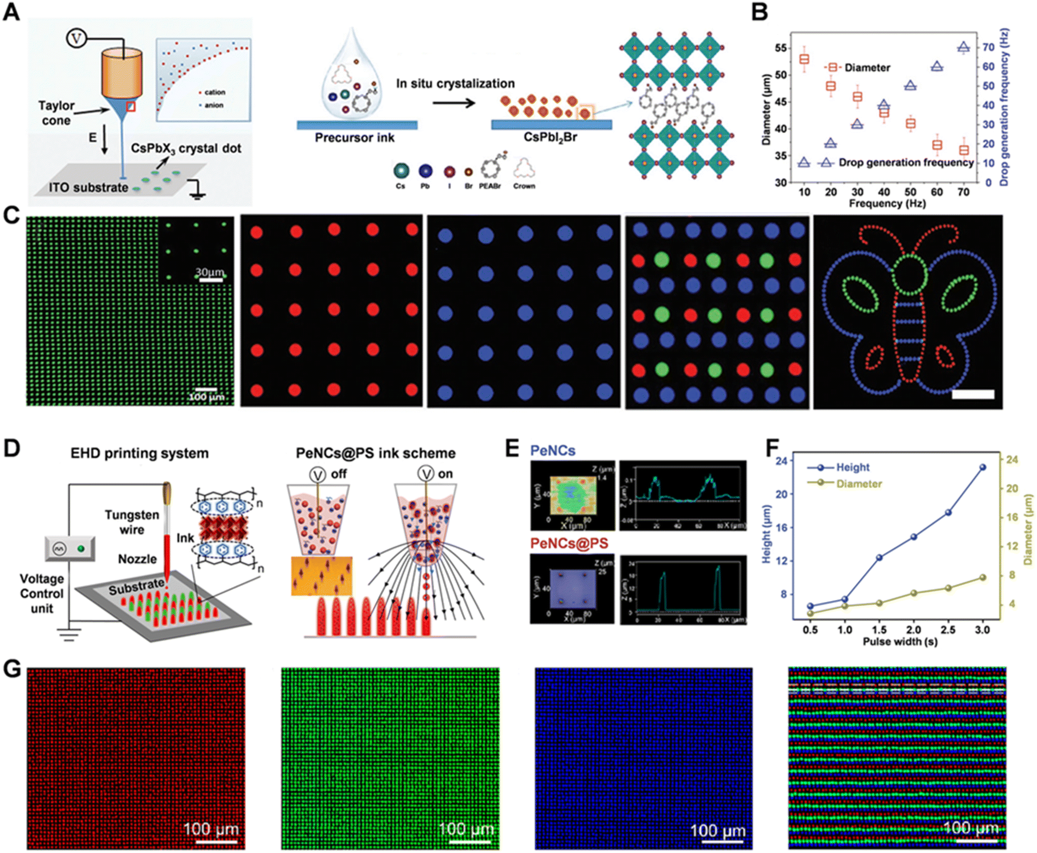 | ||
| Fig. 7 (A) Schematic of the EHD printing of perovskite precursor inks with cesium halides, lead halides and PEABr. (B) Change in the diameter of the printed QD structures and droplet generation frequency with the pulse frequency. (C) High-resolution green QD arrays and RGB single-color and multi-color patterns. Reprinted with permission from ref. 88. Copyright 2019, John Wiley and Sons. (D) Schematic of the construction of 3-dimensional color conversion QD microstructures by EHD printing of the non-polar CsPbX3 QD colloid ink with PS. (E) Height profile of the microstructures printed from colloid inks with and without PS. (F) Relationship between the height and diameter of the printed 3-dimensional microstructures with pulse width. (G) Fluorescent images of the printed RGB single color and tri-color pixels with a resolution of 2540 dpi. Reprinted with permission from ref. 90. Copyright 2024, American Chemical Society. | ||
Chen et al. used EHD inkjet printing to deposit QD color-conversion layers on nano-ring structured Micro-LED chips, creating full-color Micro-LED devices.91 They achieved a 1.65 μm minimum line width for the QD structures with excellent uniformity. Wang et al. used an eco-friendly high-viscosity ionic liquid as the solvent to prepare perovskite QD inks. With EHD inkjet printing, they produced high-resolution, flexible full-color devices with 1 μm diameter QD structures and a maximum resolution reaching approximately 5080 ppi.
EHD inkjet printing usually requires polar solvents, which can quench perovskite QDs and impair performance. Thus, developing non-polar solvent inks suitable for EHD inkjet printing is of significant importance. Yang et al. developed non-polar inks by dispersing green perovskite QDs, passivated with DDAB/PbBr2, in a 1:1 mixture of 1,3,5-triisopropylbenzene and n-tetradecane.67 Through EHD printing, they produced high-resolution QD microstructures with uniform thickness and minimized the coffee ring effect, a linewidth of 2 μm and a resolution up to 22718 ppi.
Red-perovskite QDs are less stable than green QDs, especially during EHD printing, where halide ions can migrate and affect luminescence. Yang et al. used lecithin and 1-DT as dual ligands to passivate mixed-halide CsPbBrI2 and disperse the QDs in xylene to prepare a non-polar ink.24 The dual-ligand passivation significantly enhanced the stability of red-perovskite QDs and enabled high-resolution red QD color-conversion arrays via EHD inkjet printing. The lecithin reduces damage to CsPbBrI2 under the electric field, while 1-DT passivates halide vacancies. Compared to arrays printed by using an OA/m-CsPbBrI2 ink, the arrays from the dual-ligand passivated CsPbBrI2 ink show higher brightness and a less spectral blue shift. The dual-ligand passivated CsPbBrI2 microarrays also demonstrate excellent stability during storage and UV exposure. Ultimately, they achieved a resolution of up to 2540 dpi for CsPbBrI2 red QD arrays and successfully fabricated red, green, and blue color-conversion arrays.
Chen et al. dispersed CsPbX3 QDs with polystyrene (PS) in xylene and used EHD inkjet printing to create 3D perovskite microstructure arrays.92 The PS-containing ink produced pronounced 3D structures with a height of 3 μm, while the height is only 100 nm for microstructures printed from QD ink without PS (Fig. 7E). The 3D structure morphology was controllable by adjusting the pulse width and voltage. Increasing the pulse width resulted in a change in microcolumn diameter from 2.8 μm to 7.6 μm and height from 7 μm to 24 μm (Fig. 7F). Fig. 7G shows the EHD-printed RGB monochromic and multicolor 3D QD color-conversion arrays with high resolution and excellent uniformity.
3.2. Photolithography
Photolithography is a processing technique that transfers high-precision patterns from a mask to a substrate by selectively exposing photosensitive materials and developing them in the developer.93,94 This technology is indispensable in the field of semiconductor chip manufacturing. When applied to QD patterning, lithography enables the creation of small-sized, high-precision, and large-area QD arrays, offering a reliable approach for fabricating color-conversion Micro-LED full-color display devices. Based on the variations in lithography processes, QD patterning techniques can be categorized into four types: photoresist-assisted photolithography, QD photoresist (QDPR) lithography, QD direct lithography, and QD in situ lithography.The modification of QD surfaces was adopted to improve their resistance in chemicals. Bae et al. used the bifunctional ligand mercaptopropionic acid (MPA) to passivate CdSe/ZnS core–shell QDs, minimizing QD damage during photolithography.95 This approach was applied to fabricate square and circular QD microstructure arrays. Compared to untreated CdSe/ZnS QDs, MPA-treated QD films showed a higher PL intensity before and after development, with no significant change in fluorescence lifetime.
Kim et al. used multiple atomic layer deposition (ALD) processes to passivate QDs with ZnO, improving their solvent resistance.96 The passivated QD inks were employed in photolithography to create color-conversion layers. This method achieved full-color QD arrays with a resolution of 3000 ppi and is versatile for fabricating microstructure arrays of perovskite QDs, Cd-based QDs, and InP QDs.
Lee et al. used coated a ZnO protective layer on InP QDs by an ALD technique and employed positive photoresist with a photoacid generator (PAG) to fabricate high-resolution, multicolor InP QD films by photolithography (Fig. 8A).32Fig. 8B shows the changes in the PL spectra of red and green InP QDs during the patterning processes. ZnO-passivated QD films exhibited a higher PL intensity than bare QDs, though spin-coating and developing caused damage, reducing PL intensity by 19% for red and 22% for green QD films post-patterning. The height profile in Fig. 8C shows that the thickness of the prepared QD film is 4 μm. Fig. 8D shows the prepared red and green InP QD patterns and blue ZnSeTe QD patterns, with a maximum resolution of 2000 ppi.
 | ||
| Fig. 8 (A) Schematic of the photolithographic patterning of ZnO-passivated InP QDs. (B) Intensity of green and red QDs during the pattering processes. (C) Height profile of the pattered QD microstructure. (D) Fluorescence images of the red and green InP QDs and blue ZnSeTe QD patterns. Reprinted with permission from ref. 31. Copyright 2023, American Chemical Society. | ||
Mei et al. combined a sacrificial layer-assisted patterning method with photolithography to fabricate QD color-conversion layers.97 They used polyvinylpyrrolidone as the sacrificial layer material, employing negative photoresist and the sacrificial layer to define the QD pixel positions while protecting the QDs during the photolithography process. Using this approach, they achieved RGB full-color QD pixels with dimensions of 39 μm × 5 μm, a resolution of 500 ppi, and a color gamut reaching 114% of the NTSC standard.
Myeong et al. prepared the QDPR by mixing CdSe/ZnS QDs with the negative photoresist AZ-5214E and used it to create QD color-conversion layers by photolithography (Fig. 9A).33 To reduce the light crosstalk between the subpixels, Cr patterns were prepared on the substrate before lithography of the QDPR. Repeat of the lithography of QDPRs with different colors can form multicolor patterns on the substrate. The team successfully fabricated red (Fig. 9B) and green pixel arrays with minimum linewidths down to 7 μm and a QD film thickness of approximately 5 μm. Fig. 9C shows the prepared RGB QD structures with different patterns and sizes, and the minimum linewidth of about 4–5 μm.
 | ||
| Fig. 9 (A) Schematic of the photolithographic patterning of the QDPR. (B) Microscopy images of the QD patterns with linewidths of 7 μm. (C) Fluorescence images of the RGB QD patterns. Reprinted with permission from ref. 32. Copyright 2022, Royal Society of Chemistry. (D) Fluorescence microscopic images and the CCE of QDPR films with different thicknesses before and after photolithographic pattering. (E) Microscopy images of the red and green two-color QD color conversion arrays. (F) Intensity of blue Micro-LED and color-converted Micro-LEDs with and without a black matrix. (G) Color gamut of the full-color Micro-LED display devices prepared from two-color QD color conversion layers with blue-light Micro-LED. Reprinted with permission from ref. 97. Copyright 2023, Elsevier. | ||
Chang et al. mixed SiO2-coated CdSe/ZnS QDs with the negative photoresist SU-8 3010 to create QDPR for a QD color-conversion layer.98 The SiO2 coating aids in mixing QDs with polar dispersants and photoresists while protecting the QDs. They fabricated a red-green dual-color QD array (50 μm × 50 μm) and used it in a full-color display device with blue light micro-LED backlighting. A DBR reflective layer was added to reduce blue light leakage by 99.08%. The device showed excellent stability, with less than 15% brightness decay after 500 hours at 85 °C and 90% humidity.
Weng et al. prepared a high-performance QDPR by mixing CdSe/ZnS QDs, TiO2 scattering particles, and negative photoresists, and used it to fabricate a full-color QD color-conversion layer by lithography.99 The scattering effect of TiO2 helps reduce the film's total internal reflection, enhancing blue light absorption and light conversion efficiency. Using this QDPR, the authors fabricated square red and green QD films with pixel sizes of 80 μm × 80 μm (Fig. 9D), showing improved color-conversion efficiency (CCE) compared to unpatterned films. The microscopic images in Fig. 9E show the red and green two-color QD color-conversion arrays. The authors also studied the impact of black photoresist structures on color conversion, and the results showed that the black photoresist effectively reduces light crosstalk and enhances pattern clarity. The introduction of black photoresists led to a significant reduction in the intensity of red, green, and blue light, with CCE decreases of 3.93% and 5.97% for green and red light, respectively (Fig. 9F). Upon integrating two-color QD color-conversion layers with blue light Micro-LEDs, the full-color display devices achieved a color gamut of 120.53% of the NTSC standard (Fig. 9G).
Lee et al. used a low-temperature ALD technique for passivating patterned QDPR arrays with TiO2, which enhanced QD stability under high-temperature and natural conditions.100 The prepared 7 μm × 7 μm red and green pixel arrays show uniform light when excited by the bottom blue-UV mixed micro-LED. After adding a DBR layer, the CCEs of the red and green QD color-conversion layers reached 96.25% and 92.91%, respectively, with the full-color display device achieving a color gamut of 128.2% of the NTSC standard.
Huang et al. prepared a perovskite QDPR by mixing perovskite QDs with propylene glycol methyl ether acetate (PGMEA), photoinitiators, and acrylic monomer resin.101 Original ligands, OA, were exchanged by 2-(4-chlorosulfonylphenyl)ethyltrimethoxysilane (CES) for the growth of homogenous perovskite QDs with small size and high stability. Using this perovskite QDPR, the authors achieved QD patterns with sizes smaller than 5 μm. By combining the as-prepared red and green QD color-conversion layers with a monolithic integrated micro-LED chip, the authors prepared a full-color Micro-LED display panel with a high-resolution of 3300 ppi, and a color gamut reaching 130.4% of the NTSC standard.
Ko et al. functionalized QD ligands with vinyltriphenylamine-random-azidestyrene and crosslinked QDs using PTPA-N3-SH. UV irradiation of the azide groups produced nitrene radicals, creating a crosslinked QD network within the film.102 Using the direct lithography method, the authors fabricated microstructured arrays of red CdSe/ZnCdS, green InP/ZnSeS, and blue CdZnS/ZnS QDs with excellent uniformity. Yang et al. employed a ligand crosslinking agent, 4-azido-2,3,5,6-tetrafluorobenzoic acid esters, to react with adjacent QD ligands under UV light, resulting in robust QD films. They used this technique to create RGB QD color-conversion pixels, each 4 μm × 16 μm, achieving a resolution of up to 1400 ppi.
Ko et al. replaced the original ligands (OA and OAm) of CsPbX3 QDs with photo-crosslinkable cinnamoyl polymer ligands (PCEMA-NH3X, where X = Cl, Br, and I).103 This enabled UV-induced crosslinking and pattern formation after toluene development (Fig. 10A). They successfully created defect-free circular arrays with 10 μm diameter (Fig. 10B) and large-area patterned arrays (2 cm × 8 cm) (Fig. 10C). The patterned structures remained stable after ethanol immersion (Fig. 10D). Tuning the terminal groups (–NH3Cl, Br, and I) of PCEMA ligands adjusted the wavelength of QDs across the visible spectrum. The synthesized blue, green, and red QDs were used to produce patterned arrays of blue squares (10 μm), green squares (5 μm), and red circles (10 μm), achieving a resolution of up to 10465 ppi (Fig. 10E).
 | ||
| Fig. 10 (A) Schematic of the replacement of the OA and OAm of CsPbX3 QDs with photo-crosslinkable PCEMA-NH3X for the patterning of QDs by direct photolithography. (B) Microscopic image of QD circular arrays and the corresponding photomask. (C) Large-area patterned QD arrays. (D) Immersion of the patterned structures in ethanol. (E) Fluorescence image of the patterned blue, green, and red QD arrays. Reprinted with permission from ref. 100. Copyright 2021, American Chemical Society. | ||
Liu et al. added bis-azide compounds as light-sensitive additives to perovskite QD solutions.104 UV exposure generated nitrile radicals that formed covalent C–N bonds with long alkyl chains in natural ligands OAm and OA, creating a crosslinked network between QDs. They achieved patterning with structural widths as small as 5 μm, with consistent uniformity and surface roughness before and after lithography. The perovskite QDs retained their size and crystal structure, and the team demonstrated successful patterning on flexible substrates, indicating potential for flexible displays.
Hahm et al. designed and synthesized dual-ligand passivated InP/ZnSexS1−x QDs, comprising photo-crosslinkable ligands (PXLs) and dispersing ligands (DLs).105 They used photoreactive benzoin derivatives as PXLs, which underwent crosslinking under light (365 nm, 35 mJ cm−2). The authors achieved a resolution of up to 15000 ppi for QD arrays using this QD direct lithography method.
Shin et al. employed thiol molecules as ligand crosslinkers for OA-capped QDs, utilizing thiol–ene click reactions to achieve direct lithographic patterning of InP QDs.106 Through this method, the authors successfully produced patterns with a minimum size of 5 μm, and the ligand crosslinking process resulted in a 122.9% increase in the PLQY compared to the original QD films.
Ong et al. synthesized a bidentate photo-crosslinkable ligand, which contains a photosensitive acrylate group and a carboxylic acid binding group, for direct photolithographic patterning of perovskite QDs.107 By optimizing the solvent system, concentration, and processing parameters, the authors achieved an optical density of 1.1 using a fully retained photo-crosslinked CsPbBr3 nanocrystal film with a thickness of 1.4 μm. By using a mask-free direct laser writing technology, the authors fabricated pixel patterns with a size of 20 μm. By using direct laser writing, well-defined green and red perovskite nanocrystal arrays with feature sizes down to 20 μm were obtained.
Zhang et al. developed a direct in situ lithography technique for patterning perovskite QDs using lead bromide complex-catalyzed photopolymerization.31 As shown in Fig. 11A, UV light (365 nm) initiates the photopolymerization of perovskite precursors, creating high-resolution patterns. This method integrates lead bromide complex catalysis, eliminating the need for external initiators or catalysts and avoiding potential QD damage. The process includes a final annealing step to synthesize QDs within the polymer matrix. The authors successfully created micrometer-sized patterns with uniform fluorescence intensity (Fig. 11B). The team also prepared red, green, and blue QD color-conversion patterns, achieving a minimum feature size of 5 μm, a maximum thickness of 10 μm, and a resolution up to 2450 ppi.
 | ||
| Fig. 11 (A) Schematic of the in situ lithography of perovskite QDs using lead bromide complex-catalyzed photopolymerization. (B) Fluorescence images of the RGB single-color and multi-color QD patterns. Reprinted with permission from ref. 30. Copyright 2022, Springer Nature. (C) Schematic of the in situ photolithographic patterning processes of the benzoin-grafted allyl phenolic resin FROS-BP. (D) Microscopic images of the QD microstructure arrays created from FROS-BP and FROS. (E) Fluorescence image of the QD patterns with different sizes, shapes, and uniform thicknesses. Reprinted with permission from ref. 104. Copyright 2024, American Chemical Society. | ||
Wei et al. developed an enhanced photoresist benzoin-grafted allyl phenolic resin FROS-BP by grafting photosensitive benzoin (BP) onto a silicon-modified allyl phenolic resin FROS, which improves radical confinement and selectivity in photolithography (Fig. 11C).108 For in situ photolithography, they prepared a resist using a solution of perovskite precursor, photosensitive monomer FROS-BP, and crosslinker in a polar solvent. Fig. 11D shows that the QD patterns created with FROS-BP exhibited sharp edges and precise 120° angles, compared to the less defined edges from FROS. The process enabled the fabrication of multi-color QD patterns with various sizes, shapes, and uniform thicknesses, with the smallest feature size being 20 μm, and the patterns were transferable to flexible PET substrates (Fig. 11E).
Li et al. replaced traditional DMF and DMSO solvents with the polymerizable monomer 4-acryloylmorpholine, which also served as a photopolymerization monomer.109 This approach enabled direct in situ fabrication and patterning of perovskite QDs. Using this QD ink, the authors achieved color QD patterns with a high PLQY of 90%, a minimum feature size of 5 μm, a thickness over 3 μm, and excellent fluorescence uniformity. Li et al. developed an in situ photolithography technique based on light-induced halide removal. They blended perovskite QD precursors with PMMA to create PQD precursor/polymer films.110 These films were exposed to 254 nm UV light through a mask, inducing halide removal and generating high-resolution QD patterns without the need for development or etching. The team successfully created square dot matrices with a sub-pixel width of 2 μm, and the QD films remained stable after 6 months in water.
3.3. Transfer printing technology
Transfer printing technology is an advanced micro–nanofabrication method that uses patterned transfer stamps for transferring QDs onto substrates with high precision. This technique is cost-effective, efficient, and achieves exceptionally high resolution with minimal environmental control.111–113 Currently, the precision of transfer printing technology can reach up to 2 nanometers, demonstrating its significant potential for nanoscale pattern fabrication. Transfer printing technology enables the fabrication of QD patterns with extremely high resolutions (ranging from thousands to tens of thousands of ppi). However, the thickness of these QDs typically ranges from a few nanometers to tens of nanometers, making the technology particularly suitable for electroluminescent QLED devices. Yet, fabricating QD patterns with a micrometer-scale thickness using transfer printing methods presents great challenges. This difficulty arises from the need to precisely control the thickness and uniformity of the patterns during the transfer process, which imposes stringent technical demands on the transfer printing technique.Zou et al. successfully fabricated high-resolution QD patterns with thicknesses exceeding 10 μm by combining plasma etching and transfer printing technologies.39 The pixel resolution and thickness of the QDs can be tuned through the microstructure of the transfer printing template and the etching process (Fig. 12A). In this method, due to the expansion of the PDMS stamp upon contact with the QD solvent (toluene), patterned recessive silicon was used as the master template, and a temporary substrate coated with an adhesive layer was employed to transfer the QDs from the recessive mold. The temporary substrate was then subjected to plasma etching to remove residual QDs, and the patterned QD film was finally transferred to the target substrate. The authors used this transfer printing technique to create QD arrays with varying sizes (less than 40 μm) and thicknesses (greater than 10 μm). Fig. 12B shows the fluorescence intensity distribution of 169 subpixels with a diameter of 40 μm and the fluorescence intensity distribution of individual subpixels, indicating good uniformity in both pixel arrays and individual pixels. As shown in the statistical plot, the fluorescence intensity distribution of 85% of the pixels is between 140 and 150.
 | ||
| Fig. 12 (A) Schematic of the transfer printing of high-resolution QD patterns combining with plasma etching technique. (B) Fluorescence images of the QD arrays and statistical analysis of the PL intensity of the QD pixels. (C) Images of the large-area CdSe/ZnS QD patterns on the flexible substrate. (D) Images of the blue Micro-LED chip, and color conversion red and green Micro-LED chips and their corresponding EL spectra. Reprinted with permission from ref. 38. Copyright 2023, Royal Society of Chemistry. | ||
In this study, the authors incorporated a polystyrene-block-polyisoprene-block-polystyrene (SPS) polymer into the QD ink. The polyisoprene block in SPS increases the main chain length and reduces the proportion of phenyl side chains, making SPS potentially more flexible than PS. Under the same conditions, the QD@SPS ink achieved a uniform pillar structure with a thickness of 12.97 μm, while the columnar structures from the QD@SPS ink after transfer exhibited irregularities and fractures. The authors successfully prepared QD patterns with a pixel resolution of 669 ppi and a maximum thickness of 19.74 μm, and high-resolution red-green CdSe/ZnS QD patterns on flexible substrates (Fig. 12C). QD films with thicknesses over 10 μm integrated onto blue Micro-LED chips displayed good color-conversion performance (Fig. 12D), revealing the potential of the transfer printing technology for full-color Micro-LED displays.
3.4. Electrophoretic deposition
Electrophoretic deposition is an emerging technique for fabricating QD color-conversion layers. This method leverages the ionizability of QD ligands in solutions, enabling the directed migration of QD particles under the influence of an electric field. Specifically, the electric field applied by the electrodes drives the QD particles toward electrodes with opposite charges, leading to their deposition and formation of high-quality color-conversion layers on these electrodes. This technique offers excellent controllability and precise patterning capabilities, providing an efficient and reproducible method for manufacturing QD color-conversion layers.Zhao et al. combined photolithography with electrophoretic deposition to produce large-area, full-color QD pattern arrays (Fig. 13A).34 The process involved immersing patterned electrodes sequentially in solutions of red, green, and blue CdSe/ZnS QDs in PGMEA. An electric field drove the QDs to oppositely charged electrodes, creating an RGB array. PEG-COOH-coated CdSe/ZnS QDs were used, and increasing the PEG-COOH concentration raised the zeta potential (Fig. 13B), indicating that the QD charges come from ligand ionization and can be adjusted by the ligand concentration. By varying the applied voltage and deposition time, the thickness of the patterned QDs can be precisely controlled. As the SEM images shown in Fig. 13C, the QD deposition is very uniform with no noticeable surface defects. The authors also created QD pixel arrays of various shapes, sizes, and colors by modifying electrode patterns (Fig. 13D). Using multiple deposition steps, they achieved RGB QD pixel arrays measuring 14 μm × 14 μm with a resolution of 1075 ppi.
 | ||
| Fig. 13 (A) Schematic of the electrophoretic deposition to full-color QD pattern arrays. (B) Relationship between the zeta potential of the PEG-COOH-coated CdSe/ZnS QDs with the concentration of ligand PEG-COOH. (C) SEM images of the deposited QDs with different thickness. (D) Fluorescence images of the electrophoretic deposited QD pixel arrays with different shapes and size. Reprinted with permission from ref. 33. Copyright 2021, Springer Nature. (E) Schematic of the multi-particle electrophoretic deposition for preparing CdSe/ZnS QDs with the dispersion matrix SiO2 and scatter TiO2. (F) SEM images of the co-deposited QD–SiO2 films. (G) PL intensity of QD films with and without TiO2. (H) Relationship between the PLQE of red and green co-deposited QD films with the concentration of TiO2. (I) PLQE and LCE of red and green co-deposited films with different thicknesses. (J) Fluorescence image of the red-green two-color co-deposited QD arrays. Reprinted with permission from ref. 34. Copyright 2024, American Chemical Society. | ||
Li et al. developed a multi-particle electrophoretic deposition (EPD) technique, combining CdSe/ZnS QDs with SiO2 and TiO2.35 SiO2 acts as a dispersion matrix, while TiO2 provides scattering effects (Fig. 13E). Prior to deposition, SiO2 was modified with silane-PEG-COOH to match the QD electrical properties. Higher PEG-COOH grafting rates on SiO2 increased both zeta potential and electrophoretic mobility, improving the multi-particle assembly. Co-deposited QD–SiO2 films were created with varying mobilities and analyzed through SEM, energy-dispersive spectroscopy, and Si/Cd ratio calculations, showing that 10% grafting resulted in uniform films (Fig. 13F). However, blue light leakage was observed due to incomplete excitation absorption. Introducing TiO2 enhanced blue light absorption by increasing the optical path length and scattering (Fig. 13G), and improving the PLQE and LCE. The optimal TiO2 concentrations led to PLQE values of 46% for red QD films and 43.8% for green QD films (Fig. 13H). Furthermore, the thickness of the multi-particle films was optimized to achieve better luminous performance (Fig. 13I). The technique enabled the creation of red-green two-color arrays with resolutions of 149 ppi, 568 ppi, and 1017 ppi (Fig. 13J), achieving a theoretical color gamut of 118% of the NTSC standard.
3.5. Microfluidic technology
Microfluidic technology involves the precise manipulation of fluids within micro- and nanoscale channels and their applications. This technology has found widespread use in fields such as chemistry, biology, and medicine.114 The notable advantages of microfluidic technology include minimal sample volume, high precision, low cost, and rapid fabrication, making microfluidic-based QD patterning a viable and practical solution. By utilizing microfluidic technology, researchers can precisely control fluid flow on a small scale, achieving high-precision QD patterning and providing a more efficient and economical solution for related applications.Li et al. used microfluidic technology to create QD color-conversion layers for Micro-LED displays.36 They introduced red CsPbBrI2 and green CsPbBr3 perovskite QDs into microchannels via syringe. A volatile solvent, n-hexane, was utilized to form solid QD films, and the channels were sealed after evaporation to protect the quantum dots from air and moisture. The resulting QDs emitted at wavelengths of 514 nm and 625 nm have narrow linewidths and high PLQE. The size of the QD arrays was measured to be 140 μm × 50 μm and the full-color display device achieved a color gamut of 131% of the NTSC standard.
In another work, Li et al. fabricated flexible QD color-conversion layers using microfluidic technology. The sealing layer and microchannels were both fabricated from PDMS. After treating with oxygen plasma, the microchannels are aligned and bonded with the sealing layer to enhance the success rate of the color-conversion layer fabrication. Subsequently, red and green perovskite QDs are dispersed in n-hexane and introduced into the microchannels to complete the fabrication of the color-conversion layer. Further studies investigated the impact of bending radius on the performance of the microfluidic flexible color-conversion layer. At a bending radius of 15 mm, the emission intensity of red and green pixels changed by 26% and 3%, respectively. After 1000 bending cycles, the emission intensity changes were 29% and 5% for red and green pixels, respectively, with color gamut variations of less than 4%.
Weng et al. used a microfluidic technology to create patterned QD color-conversion films.115 Vacuum suction guides resin into the microchannel to form the pattern after photochemical or thermal curing. The addition of polymers to the QD solution demonstrated to reduce the defect of patterned QD films after drying. Using this technology, the authors produced red and green QD patterned films with a linewidth of 8 μm and a thickness of 5 μm.
Due to the lack of complete isolation between the pixels, the prepared pixels suffered from color crosstalk between the adjacent subpixels. To solve this, Zhu et al. developed a static droplet array (SDA) microfluidic technology for creating separate color-conversion QD arrays (Fig. 14A).38 In this approach, red and green CdSe/ZnS QD solutions are introduced separately into SDA microchannels. Capillary forces guide the QDs into circular pixel areas through bridge structures. Transparent silicone oil, immiscible with the QD solution, is then injected to remove the QDs, creating a uniformly sized and separated two-color QD array. The entire process takes only 257 seconds (Fig. 14B). Using the SDA microfluidic technology, the authors produced droplets from 1 to 100 μm. As shown in Fig. 14C, the 20 μm red-green monochrome and two-color QD arrays demonstrate high optical uniformity and minimal crosstalk. The uniformity of 20 μm QD pixels is 98.58% and 98.72% for red and green, respectively.
 | ||
| Fig. 14 (A) Schematic of the SDA system for creating color conversion layers by using microfluidic technology. (B) Processes of the injection of red QD solution, green QD solution, and silicone oil for generating separate two-color QD arrays. (C) Green and red monochrome and two-color QD arrays and the corresponding PL intensity. Reprinted with permission from ref. 37. Copyright 2023, Royal Society of Chemistry. | ||
3.6. Micropore filling method
The micropore filling method involves the creation of patterned arrays with micrometer-scale thickness and filling of QDs into these patterned arrays. This method allows for the construction of color-conversion arrays of a single color with a single filling step. To fabricate multicolor QD color-conversion layers, this filling process can be repeated. Notably, the micropore filling method causes minimal damage to the QDs, which helps to maintain their excellent photoluminescence properties, making it a valuable approach for preserving the QD performance.Huang et al. used the micropore filling method to fabricate QD color-conversion layers.40 They created a patterned micropore array on a substrate via photolithography and then spin-coated CdSe QDs and removed excess materials to complete the layer. Additionally, the QDs can be further protected by SiO2 or Si3N4 dielectric layers. The team produced rectangular QD arrays with widths of 5 μm, 10 μm, 15 μm, and 20 μm. Long-term stability tests showed that the CCE of arrays decreased by only 14.9% over 5980 hours, suggesting a device lifetime of approximately 12830 hours.
Sun et al. employed the micropore filling method to deposit perovskite QDs with pixel sizes from 2 μm to 100 μm.41 They created a micropore array on an SU-8 film via photolithography, filled it with QDs using spin-coating and polished away excess QDs (Fig. 15A). This method supports diverse perovskite QD patterns and adjustable pixel thicknesses by altering the SU-8 mold. The authors achieved green pixel arrays with up to 849 ppi resolution on a 2-inch glass substrate (Fig. 15B), with the smallest pixel size of 2 μm. Fluorescence analysis of 3136 pixels showed a uniformity of 3.22 ± 0.61%, indicating excellent optical consistency (Fig. 15C). Finally, the authors created red-green dual-color QD layers, with pixel sizes of 10 μm × 10 μm and 10 μm × 30 μm (Fig. 15D).
 | ||
| Fig. 15 (A) Schematic of the preparation of QD arrays by filling the SU-8 micropore arrays with QDs, scraping the excess QD film and polishing the composite. (B) Fluorescence image of the prepared green QD pixel arrays. (c) Statistical analysis of the PL intensity of the prepared pixels. (D) Red-green dual-color QD arrays after repeating the micropore filling, scraping and polishing processes. Reprinted with permission from ref. 40. Copyright 2022, Royal Society of Chemistry. (E) Schematic and the fluorescence images of the perovskite color conversion layers in the glass micropore arrays on blue Micro-LED chip. (F) Color gamut of the full-color Micro-LED display device prepared from blue Micro-LED, green QDs arrays, and bi-component red emissive QD. Reprinted with permission from ref. 41. Copyright 2023, John Wiley and Sons. | ||
Fan et al. combined dual-component red perovskite QDs with the micropore filling method to fabricate QD color-conversion layers (Fig. 15E).42 The team deposited CsPbBr3 QDs and dual-component red QDs into a glass micropore array with a pixel size of 10 μm, and used a corresponding-sized Micro-LEDs as the excitation source. Fig. 15E shows the microscopy images of the color-conversion layer and the blue Micro-LED arrays. The color theoretical gamut of the Micro-LED device made from the blue LED, green perovskite QD, and dual-component red QDs reached 135.90% of the NTSC standard (Fig. 15F).
4. Conclusions and perspective
In this article, we comprehensively reviewed the latest achievements in QD materials and their patterning technologies for full-color Micro-LED displays. First, we talked the commonly used II–VI group QD, III–V group QD, and perovskite QD materials in Micro-LED display applications, and generally utilized ligand engineering, coating technologies, and construction of core–shell structures for improving the luminescence intensity and stability of these QDs. Then, we systematically elaborated on the latest research in QD patterning technologies including inkjet printing, photolithography, electrophoretic deposition, microfluidic techniques, transfer printing, and micropore filling method. These patterning methods all possess their advantages and limitations. With the advancement of QD color-conversion Micro-LED technology, future research will focus on enhancing the display quality, reducing costs, and improving the production efficiency. The following is our outlook upon the future development of the QD patterning technique specialized at color-conversion Micro-LED displays.(1) Inkjet printing provides a high-resolution and high-material-utilization technique for patterning QDs. In particular, the EHD printing technique can be used to prepare QD pixels with a resolution over 20000 dpi. However, the QD arrays are prepared by inkjet printing usually with a height of hundreds of nanometres, which lead to relatively low CCE and severe excitation light leakage. Therefore, the optimization of QD inks specialized for inkjet printing and printing parameters is essential to prepare high-resolution and 3-dimensional QD pixels with a height of several micrometers and enough QD concentration. For the construction of high-resolution patterned black matrix, accurate and continuous inkjet printing of QD is helpful to reduce the excitation light leakage and color crosstalk between the pixels.
(2) Photolithography can be used to prepare high-resolution QD color-conversion structures in large areas in a high-throughput manner. The direct photolithography can reduce the damage of lithographic patterning processes on the QDs, which is vital in practical applications. However, the mass utilization of the QDs in lithographic patterning is low, which increases the display production costs. Combining with other patterning techniques such as inkjet printing to pre-deposit the QDs on the substrate and further pattering them with lithography may provide alternative solutions for increasing the QD utilization ratio.
(3) Electrophoretic deposition provides a fast deposition technique for QD patterns with controllable thickness. This technique requires the construction of electrodes on the substrate through photolithography and metal or metal oxide deposition. Although the microscopy images of the QDs show regular shapes, the neighbor pixels with the same color were connected by QDs with narrow linewidth due to the existence of underlying electrode. Therefore, a more rational design of the electrodes is required for depositing absolutely separated QD pixels for decreasing the potential color-crosstalk.
(4) Microfluidic technology shows its potential for constructing QD color-conversion arrays with a high material utilization efficiency. However, this technique needs to prepare mold and microfluidic chips, which makes this method beneficial if the microfluidic chips can be utilized repeatedly to reduce the cost. In addition, this method needs to prove its potential in patterning QDs in a large area, which requires the optimization of the physicochemical properties of the microfluidic chips and rheological properties of the QD inks.
(5) Transfer printing has shown its potential in the patterning of single-color and multi-color QDs with a micrometer thickness. To date, the highest resolution of the transfer printed QD arrays with high thickness is limited to several hundred ppi. With the aim to apply Micro-LED displays in AR, VR, etc., the resolution of the transfer printed QD arrays needs to be further increased.
(6) Micropore filling method provides a straightforward and simple method to prepare large-area QD patterns. The damage of this patterning technique for QDs is low, but only color-conversion structures were demonstrated. In the future, the accurate alignment and bonding of the large-area multi-color QD color-conversion layer and Micro-LED chip are required to prove the commercial potential of the micropore filling method.
Besides the high PL intensity, PLQY, and the stability of QDs, the patterning techniques require the QDs to possess some specific properties such as the rheological properties for inkjet printing, photoactivity of the ligands for lithography, and charge of the QDs for electrophoretic deposition. Therefore, the preparation of high-quality QDs and patterning techniques are highly correlated. Through continuous technological innovation and improvement in QD synthesis and pattering techniques, QD-based color-conversion Micro-LED displays are expected to play a more significant role in the future display technology.
Data availability
A data availability statement (DAS) is required to be submitted alongside all articles. Please read our full guidance on data availability statements for more details and examples of suitable statements you can use.Conflicts of interest
There are no conflicts to declare.Acknowledgements
This work is supported by the National Natural Science Foundation of China (62374142), Fundamental Research Funds for the Central Universities (20720220085 and 20720240064), External Cooperation Program of Fujian (2022I0004), Major Science and Technology Project of Xiamen in China (3502Z20191015), Xiamen Natural Science Foundation Youth Project (3502Z202471002).References
- Y. Huang, E.-L. Hsiang, M.-Y. Deng and S.-T. Wu, Light: Sci. Appl., 2020, 9, 105 CrossRef CAS PubMed.
- T. Wu, C.-W. Sher, Y. Lin, C.-F. Lee, S. Liang, Y. Lu, S.-W. Huang Chen, W. Guo, H.-C. Kuo and Z. Chen, Appl. Sci., 2018, 8, 1557 CrossRef.
- Y. Zheng, Y. Yu, W. Chen, H. Hu, T. Guo and F. Li, Sci. China Mater., 2023, 66, 2128–2145 CrossRef.
- W. C. Miao, F. H. Hsiao, Y. Sheng, T. Y. Lee, Y. H. Hong, C. W. Tsai, H. L. Chen, Z. Liu, C. L. Lin, R. J. Chung, Z. T. Ye, R. H. Horng, S. C. Chen, H. C. Kuo and J. H. He, Adv. Opt. Mater., 2023, 12, 2300112 CrossRef.
- J. Chen, Q. Zhao, B. Yu and U. Lemmer, Adv. Opt. Mater., 2023, 12, 2300873 CrossRef.
- G. Wang, A. Badal, X. Jia, J. S. Maltz, K. Mueller, K. J. Myers, C. Niu, M. Vannier, P. Yan, Z. Yu and R. Zeng, Nat. Mach. Intell., 2022, 4, 922–929 CrossRef PubMed.
- G. H. Lee, K. Kim, Y. Kim, J. Yang and M. K. Choi, Nano–Micro Lett., 2023, 16, 45 CrossRef PubMed.
- Z. Liu, C.-H. Lin, B.-R. Hyun, C.-W. Sher, Z. Lv, B. Luo, F. Jiang, T. Wu, C.-H. Ho, H.-C. Kuo and J.-H. He, Light: Sci. Appl., 2020, 9, 83 CrossRef CAS PubMed.
- S. Zhang, H. Zheng, L. Zhou, H. Li, Y. Chen, C. Wei, T. Wu, W. Lv, G. Zhang, S. Zhang, Z. Gong, B. Jia, H. Lin, Z. Gao, W. Xu and H. Ning, Crystals, 2023, 13, 1001 CrossRef CAS.
- J. Park, J. H. Choi, K. Kong, J. H. Han, J. H. Park, N. Kim, E. Lee, D. Kim, J. Kim, D. Chung, S. Jun, M. Kim, E. Yoon, J. Shin and S. Hwang, Nat. Photonics, 2021, 15, 449–455 CrossRef CAS.
- X. Yang, Y. Lin, T. Wu, Z. Yan, Z. Chen, H.-C. Kuo and R. Zhang, Opto-Electron. Adv., 2022, 5, 210123–210123 CAS.
- S. J. Park, C. Keum, H. Zhou, T. W. Lee, W. Choe and H. Cho, Adv. Mater. Technol., 2023, 8, 2201070 CrossRef CAS.
- T. Ma, J. Chen, Z. Chen, L. Liang, J. Hu, W. Shen, Z. Li and H. Zeng, Adv. Mater. Technol., 2022, 8, 2200632 CrossRef.
- J. E. Ryu, S. Park, Y. Park, S. W. Ryu, K. Hwang and H. W. Jang, Adv. Mater., 2023, 35, 2204947 CrossRef CAS PubMed.
- B. H. Yu, Y. Li, J. S. Li, X. R. Ding and Z. T. Li, J. Phys. D: Appl. Phys., 2024, 57, 463001 CrossRef CAS.
- H. H. He, J. P. Huang, T. Tao, T. Zhi, K. X. Zhang, Z. Zhuang, Y. Yan and B. Liu, Nanomaterials, 2024, 14, 511 CrossRef CAS PubMed.
- A. R. Anwar, M. T. Sajjad, M. A. Johar, C. A. Hernández-Gutiérrez, M. Usman and S. P. Łepkowski, Laser Photonics Rev., 2022, 16, 2100427 CrossRef.
- X. Wang, Z. Bao, Y.-C. Chang and R.-S. Liu, ACS Energy Lett., 2020, 5, 3374–3396 CrossRef CAS.
- G. Yang, X. Zhou, Z. Gao, J. Shi, T. Li, S. Wei, P. Huang and P. Zhang, Angew. Chem., Int. Ed., 2024, e202413741 Search PubMed.
- Y.-M. Huang, K. James Singh, T.-H. Hsieh, C. Langpoklakpam, T.-Y. Lee, C.-C. Lin, Y. Li, F.-C. Chen, S.-C. Chen, H.-C. Kuo and J.-H. He, Nanoscale, 2022, 14, 4042–4064 RSC.
- J. Fan, C. Han, G. Yang, B. Song, R. Xu, C. Xiang, T. Zhang and L. Qian, Adv. Mater., 2024, 2312948 CrossRef CAS PubMed.
- K. Agarwal, H. Rai and S. Mondal, Mater. Res. Express, 2023, 10, 062001 CrossRef CAS.
- J. Yang, M. K. Choi, U. J. Yang, S. Y. Kim, Y. S. Kim, J. H. Kim, D.-H. Kim and T. Hyeon, Nano Lett., 2020, 21, 26–33 CrossRef PubMed.
- X. Yang, S. Wang, Y. Hou, Y. Wang, T. Zhang, Y. Chen, G. Chen, C. Zhong, X. Fan, X. Kong, T. Wu, Y. Lu, Y. Lin and Z. Chen, Nano Lett., 2024, 24, 3661–3669 CrossRef CAS PubMed.
- L. Shi, L. Meng, F. Jiang, Y. Ge, F. Li, X. g. Wu and H. Zhong, Adv. Funct. Mater., 2019, 29, 1903648 CrossRef.
- J. Cai, W. Lai, Y. Chen, X. Zhang, Y. Zheng, W. Zhang, X. Chen, Y. Ye, S. Xu, Q. Yan, T. Guo and E. Chen, Laser Photonics Rev., 2024, 2400298 CrossRef CAS.
- H.-Y. Lin, C.-W. Sher, D.-H. Hsieh, X.-Y. Chen, H.-M. P. Chen, T.-M. Chen, K.-M. Lau, C.-H. Chen, C.-C. Lin and H.-C. Kuo, Photonics Res., 2017, 5, 411 CrossRef CAS.
- S. Kim, S. Kang, S. Baek, J. Song, N.-E. Mun, H. Kwon, H.-G. Kwon, Y.-J. Pu, T.-W. Lee, S. Yoo, J.-M. Oh, J. Park and S.-W. Kim, Chem. Eng. J., 2022, 441, 135991 CrossRef CAS.
- Y. Q. Zheng, Y. Y. Duan, Y. Ye, X. K. Zheng, A. C. Du, E. G. Chen, S. Xu and T. L. Guo, Luminescence, 2024, 39, e4691 CrossRef CAS PubMed.
- H. Cho, J. A. Pan, H. Wu, X. Lan, I. Coropceanu, Y. Wang, W. Cho, E. A. Hill, J. S. Anderson and D. V. Talapin, Adv. Mater., 2020, 32, e2003805 CrossRef PubMed.
- P. Zhang, G. Yang, F. Li, J. Shi and H. Zhong, Nat. Commun., 2022, 13, 6713 CrossRef CAS PubMed.
- J. Y. Lee, E. A. Kim, Y. Choi, J. Han, D. Hahm, D. Shin, W. K. Bae, J. Lim and S.-Y. Cho, ACS Photonics, 2023, 10, 2598–2607 CrossRef CAS.
- S. Myeong, B. Chon, S. Kumar, H.-J. Son, S. O. Kang and S. Seo, Nanoscale Adv., 2022, 4, 1080–1087 RSC.
- J. Zhao, L. Chen, D. Li, Z. Shi, P. Liu, Z. Yao, H. Yang, T. Zou, B. Zhao, X. Zhang, H. Zhou, Y. Yang, W. Cao, X. Yan, S. Zhang and X. W. Sun, Nat. Commun., 2021, 12, 4603 CrossRef CAS PubMed.
- X. Li, J. Zhao, H. Xiao, H. Zhang, M. Zhou, X. Zhang, X. Yan, A. Tang and L. Chen, ACS Nano, 2024, 18, 17715–17724 CrossRef CAS PubMed.
- Y. Li, J. Tao, Q. Wang, Y. Zhao, Y. Sun, P. Li, J. Lv, Y. Qin, W. Wang, Q. Zeng and J. Liang, Appl. Phys. Lett., 2021, 118, 173501 CrossRef CAS.
- P. Li, J. Tao, Y. Zhao, Y. Sun, K. Fan, L. Zhu, W. Sun, J. Lv, Y. Qin, Q. Wang, Q. Zeng, W. Wang, S. Wang and J. Liang, Micromachines, 2022, 13, 448 CrossRef PubMed.
- L. Zhu, J. Tao, P. Li, W. Sun, J. Li, K. Fan, J. Lv, Y. Qin, K. Zheng, B. Zhao, Y. Zhao, Y. Chen, Y. Tang, W. Wang and J. Liang, Nanoscale Adv., 2023, 5, 2743–2747 RSC.
- S. Zou, Y. Li and Z. Gong, Nanoscale, 2023, 15, 18317–18327 RSC.
- C.-C. Lin, Y.-H. Fang, M.-J. Kao, P.-K. Huang, F.-P. Chang, L.-C. Yang and C.-I. Wu, SID Int. Symp. Dig. Tech. Pap., 2018, 49, 782–785 CrossRef CAS.
- W. Sun, F. Li, J. Tao, P. Li, L. Zhu, J. Li, J. Lv, W. Wang, J. Liang and H. Zhong, Nanoscale, 2022, 14, 5994–5998 RSC.
- X. Fan, S. Wang, X. Yang, C. Zhong, G. Chen, C. Yu, Y. Chen, T. Wu, H. C. Kuo, Y. Lin and Z. Chen, Adv. Mater., 2023, 35, 2300834 CrossRef CAS PubMed.
- K. Gong, Y. Zeng and D. F. Kelley, J. Phys. Chem. C, 2013, 117, 20268–20279 CrossRef CAS.
- N. Ben Brahim, N. Bel Haj Mohamed, M. Poggi, R. Ben Chaâbane, M. Haouari, H. Ben Ouada and M. Negrerie, Sens. Actuators, B, 2017, 243, 489–499 CrossRef CAS.
- J. Osinski and P. Palomaki, SID Int. Symp. Dig. Tech. Pap., 2019, 50, 34–37 CrossRef CAS.
- K. Nasirzadeh, S. Nazarian and S. M. G. Hayat, J. Appl. Biotechnol. Rep., 2016, 3, 395–402 CAS.
- W. Nan, Y. Niu, H. Qin, F. Cui, Y. Yang, R. Lai, W. Lin and X. Peng, J. Am. Chem. Soc., 2012, 134, 19685–19693 CrossRef CAS PubMed.
- K.-P. Chang, Y.-C. Yeh, C.-J. Wu, C.-C. Yen and D.-S. Wuu, Nanomaterials, 2022, 12, 909 CrossRef CAS PubMed.
- C. B. Murray, D. J. Norris and M. G. Bawendi, J. Am. Chem. Soc., 1993, 115, 8706–8715 CrossRef CAS.
- W. W. Yu and X. Peng, Angew. Chem., Int. Ed., 2002, 41, 2368–2371 CrossRef CAS PubMed.
- C. Pu, J. Zhou, R. Lai, Y. Niu, W. Nan and X. Peng, Nano Res., 2013, 6, 652–670 CrossRef CAS.
- D. V. Talapin, A. L. Rogach, A. Kornowski, M. Haase and H. Weller, Nano Lett., 2001, 1, 207–211 CrossRef CAS PubMed.
- I. Mekis, D. V. Talapin, A. Kornowski, M. Haase and H. Weller, J. Phys. Chem. B, 2003, 107, 7454–7462 CrossRef CAS.
- J. J. Li, Y. A. Wang, W. Guo, J. C. Keay, T. D. Mishima, M. B. Johnson and X. Peng, J. Am. Chem. Soc., 2003, 125, 12567–12575 CrossRef CAS PubMed.
- L. Lv, J. Li, Y. Wang, Y. Shu and X. Peng, J. Am. Chem. Soc., 2020, 142, 19926–19935 CrossRef CAS PubMed.
- J. Zhang, C. Li, J. Li and X. Peng, Chem. Mater., 2023, 35, 7049–7059 CrossRef CAS.
- J. Shamsi, A. S. Urban, M. Imran, L. De Trizio and L. Manna, Chem. Rev., 2019, 119, 3296–3348 CrossRef CAS PubMed.
- X. Mei, D. Jia, J. Chen, S. Zheng and X. Zhang, Nano Today, 2022, 43, 101449 CrossRef CAS.
- L. Protesescu, S. Yakunin, M. I. Bodnarchuk, F. Krieg, R. Caputo, C. H. Hendon, R. X. Yang, A. Walsh and M. V. Kovalenko, Nano Lett., 2015, 15, 3692–3696 CrossRef CAS PubMed.
- Q. Chang, X. Zhou, S. Jiang, G. Xiang, L. Li, Y. Li, C. Jing, F. Ling, Y. Wang and P. Xiao, Ceram. Int., 2022, 48, 33645–33652 CrossRef CAS.
- J. S. Shaikh, N. S. Shaikh, S. S. Mali, J. V. Patil, S. A. Beknalkar, A. P. Patil, N. L. Tarwal, P. Kanjanaboos, C. K. Hong and P. S. Patil, ChemSusChem, 2019, 12, 4724–4753 CrossRef CAS PubMed.
- J. I. Kim, Q. Zeng, S. Park, H. Lee, J. Park, T. Kim and T. W. Lee, Adv. Mater., 2023, 35, 2209784 CrossRef CAS PubMed.
- J. Cai, X. Zhang, Y. Chen, W. Lai, W. Zhang, Z. Lin, Y. Ye, S. Xu, T. Guo, J. Luo and E. Chen, J. Lumin., 2024, 269, 120508 CrossRef CAS.
- S. Li, Z. Shi, F. Zhang, L. Wang, Z. Ma, D. Yang, Z. Yao, D. Wu, T.-T. Xu, Y. Tian, Y. Zhang, C. Shan and X. J. Li, Chem. Mater., 2019, 31, 3917–3928 CrossRef CAS.
- M. Liu, N. Jiang, H. Huang, J. Lin, F. Huang, Y. Zheng and D. Chen, Chem. Eng. J., 2021, 413, 127547 CrossRef CAS.
- W. J. Mir, A. Alamoudi, J. Yin, K. E. Yorov, P. Maity, R. Naphade, B. Shao, J. Wang, M. N. Lintangpradipto, S. Nematulloev, A.-H. Emwas, A. Genovese, O. F. Mohammed and O. M. Bakr, J. Am. Chem. Soc., 2022, 144, 13302–13310 CrossRef CAS PubMed.
- X. Yang, Z. J. Yan, C. M. Zhong, H. Jia, G. L. Chen, X. T. Fan, S. L. Wang, T. Z. Wu, Y. Lin and Z. Chen, Adv. Opt. Mater., 2023, 11, 2202673 CrossRef CAS.
- M. Xie, J. Guo, X. Zhang, C. Bi, X. Sun, H. Li, L. Zhang, D. Binks, G. Li, W. Zheng and J. Tian, Adv. Funct. Mater., 2023, 33, 2300116 CrossRef CAS.
- C. Li, J. Yao, L. Xu, Z. Yang, S. Wang, B. Cai, J. Wang, W. Fan, Y. Wang and J. Song, Chem. Eng. J., 2024, 493, 152483 CrossRef CAS.
- Y. Li, M. Deng, X. Zhang, T. Xu, X. Wang, Z. Yao, Q. Wang, L. Qian and C. Xiang, Nat. Commun., 2024, 15, 5696 CrossRef CAS PubMed.
- S. Huang, Z. Li, L. Kong, N. Zhu, A. Shan and L. Li, J. Am. Chem. Soc., 2016, 138, 5749–5752 CrossRef CAS PubMed.
- W. Song, Y. Wang, B. Wang, Y. Yao, W. Wang, J. Wu, Q. Shen, W. Luo and Z. Zou, Nano Res., 2020, 13, 795–801 CrossRef CAS.
- M. He, Q. Zhang, F. Carulli, A. Erroi, W. Wei, L. Kong, C. Yuan, Q. Wan, M. Liu, X. Liao, W. Zhan, L. Han, X. Guo, S. Brovelli and L. Li, ACS Energy Lett., 2022, 8, 151–158 CrossRef.
- D. B. Berkinsky, A. H. Proppe, H. Utzat, C. J. Krajewska, W. Sun, T. Šverko, J. J. Yoo, H. Chung, Y.-H. Won, T. Kim, E. Jang and M. G. Bawendi, ACS Nano, 2023, 17, 3598–3609 CrossRef CAS PubMed.
- P. Yu, Y. Shan, S. Cao, Y. Hu, Q. Li, R. Zeng, B. Zou, Y. Wang and J. Zhao, ACS Energy Lett., 2021, 6, 2697–2703 CrossRef CAS.
- J.-H. Jo, D.-Y. Jo, S.-H. Lee, S.-Y. Yoon, H.-B. Lim, B.-J. Lee, Y. R. Do and H. Yang, ACS Appl. Nano Mater., 2020, 3, 1972–1980 CrossRef CAS.
- K.-H. Kim, J.-H. Jo, D.-Y. Jo, C.-Y. Han, S.-Y. Yoon, Y. Kim, Y.-H. Kim, Y. H. Ko, S. W. Kim, C. Lee and H. Yang, Chem. Mater., 2020, 32, 3537–3544 CrossRef CAS.
- J. J. Calvin, J. K. Swabeck, A. B. Sedlak, Y. Kim, E. Jang and A. P. Alivisatos, J. Am. Chem. Soc., 2020, 142, 18897–18906 CrossRef CAS PubMed.
- W. Zhang, Y. Tan, X. Duan, F. Zhao, H. Liu, W. Chen, P. Liu, X. Liu, K. Wang, Z. Zhang and X. W. Sun, Adv. Opt. Mater., 2022, 10, 2200685 CrossRef CAS.
- Q. Wu, F. Cao, S. Wang, Y. Wang, Z. Sun, J. Feng, Y. Liu, L. Wang, Q. Cao, Y. Li, B. Wei, W. Y. Wong and X. Yang, Adv. Sci., 2022, 9, 2200959 CrossRef CAS PubMed.
- H. Li, Y. Bian, W. Zhang, Z. Wu, T. K. Ahn, H. Shen and Z. Du, Adv. Funct. Mater., 2022, 32, 2204529 CrossRef CAS.
- P. Yu, S. Cao, Y. Shan, Y. Bi, Y. Hu, R. Zeng, B. Zou, Y. Wang and J. Zhao, Light: Sci. Appl., 2022, 11, 162 CrossRef CAS PubMed.
- F. Mathies, E. J. W. List-Kratochvil and E. L. Unger, Energy Technol., 2019, 8, 1900991 CrossRef.
- X. Liu, J. Li, P. Zhang, W. Lu, G. Yang, H. Zhong and Y. Zhao, Nano Res., 2022, 15, 7681–7687 CrossRef CAS.
- C. Wei, W. Su, J. Li, B. Xu, Q. Shan, Y. Wu, F. Zhang, M. Luo, H. Xiang, Z. Cui and H. Zeng, Adv. Mater., 2022, 34, 2107798 CrossRef CAS PubMed.
- Y. Wang, Y. Yin, M. Liu, M. U. Ali and H. Meng, Laser Photonics Rev., 2024, 2300962 CrossRef CAS.
- S. Y. Lee, C. Sakong, S. H. Choi, B. K. Ju and K. H. Cho, Adv. Mater. Interfaces, 2022, 10, 2201851 CrossRef.
- C. Oakley and P. Chahal, IEEE Trans. Terahertz Sci. Technol., 2018, 8, 765–772 CAS.
- H.-V. Han, H.-Y. Lin, C.-C. Lin, W.-C. Chong, J.-R. Li, K.-J. Chen, P. Yu, T.-M. Chen, H.-M. Chen, K.-M. Lau and H.-C. Kuo, Opt. Express, 2015, 23, 32504–32515 CrossRef CAS PubMed.
- M. Zhu, Y. Duan, N. Liu, H. Li, J. Li, P. Du, Z. Tan, G. Niu, L. Gao, Y. Huang, Z. Yin and J. Tang, Adv. Funct. Mater., 2019, 29, 1903294 CrossRef.
- S.-W. Huang Chen, C.-C. Shen, T. Wu, Z.-Y. Liao, L.-F. Chen, J.-R. Zhou, C.-F. Lee, C.-H. Lin, C.-C. Lin, C.-W. Sher, P.-T. Lee, A.-J. Tzou, Z. Chen and H.-C. Kuo, Photonics Res., 2019, 7, 416–422 CrossRef.
- Y. Chen, X. Yang, X. Fan, A. Kang, X. Kong, G. Chen, C. Zhong, Y. Lu, Y. Fan, X. Hou, T. Wu, Z. Chen, S. Wang and Y. Lin, ACS Appl. Mater. Interfaces, 2024, 16, 24908–24919 CrossRef CAS PubMed.
- Z. Y. Gao, J. B. Shi and G. L. Yang, Adv. Opt. Mater., 2024, 2401106 CrossRef CAS.
- W. Guo, J. Chen, T. Ma, Z. Chen, M. Li, H. Zeng and J. Lu, Adv. Funct. Mater., 2023, 34, 2310338 CrossRef.
- J. H. Bae, S. Kim, J. Ahn, C. Shin, B. K. Jung, Y. M. Lee, Y. K. Hong, W. Kim, D. H. Ha, T. N. Ng, J. Kim and S. J. Oh, ACS Appl. Mater. Interfaces, 2022, 14, 47831–47840 CrossRef CAS PubMed.
- G.-H. Kim, J. Lee, J. Y. Lee, J. Han, Y. Choi, C. J. Kang, K.-B. Kim, W. Lee, J. Lim and S.-Y. Cho, ACS Appl. Mater. Interfaces, 2021, 13, 43075–43084 CrossRef CAS PubMed.
- W. Mei, Z. Zhang, A. Zhang, D. Li, X. Zhang, H. Wang, Z. Chen, Y. Li, X. Li and X. Xu, Nano Res., 2020, 13, 2485–2491 CrossRef CAS.
- K.-P. Chang, C.-J. Wu, C.-W. Lo, Y.-S. Lin, C.-C. Yen and D.-S. Wuu, Mater. Sci. Semicond. Process., 2022, 148, 106790 CrossRef CAS.
- Y. Weng, G. Chen, X. Zhou, Y. Zhang, Q. Yan and T. Guo, J. Lumin., 2023, 261, 119892 CrossRef CAS.
- T.-Y. Lee, W.-C. Miao, Y.-Y. Hung, Y.-H. Bai, P.-T. Chen, W.-T. Huang, K.-A. Chen, C.-C. Lin, F.-C. Chen, Y.-H. Hong and H.-C. Kuo, Nanomaterials, 2023, 13, 2099 CrossRef CAS PubMed.
- J. Huang, Z. Li, Y. Zhu, L. Yang, X. Lin, Y. Li, Y. Wang, Y. Wang, Y. Fu, W. Xu, M. Huang, D. Li and A. Pan, Adv. Mater., 2024, 36, 2409025 CrossRef CAS PubMed.
- J. Ko, J. H. Chang, B. G. Jeong, H. J. Kim, J. F. Joung, S. Park, D. H. Choi, W. K. Bae and J. Bang, ACS Appl. Mater. Interfaces, 2020, 12, 42153–42160 CrossRef PubMed.
- J. Ko, K. Ma, J. F. Joung, S. Park and J. Bang, Nano Lett., 2021, 21, 2288–2295 CrossRef CAS PubMed.
- D. Liu, K. K. Weng, S. Y. Lu, F. Li, H. Abudukeremu, L. P. Zhang, Y. C. Yang, J. Y. Hou, H. W. Qiu, Z. Fu, X. Y. Luo, L. Duan, Y. Y. Zhang, H. Zhang and J. H. Li, Sci. Adv., 2022, 8, eabm8433 CrossRef CAS PubMed.
- D. Hahm, J. Lim, H. Kim, J.-W. Shin, S. Hwang, S. Rhee, J. H. Chang, J. Yang, C. H. Lim, H. Jo, B. Choi, N. S. Cho, Y.-S. Park, D. C. Lee, E. Hwang, S. Chung, C.-m. Kang, M. S. Kang and W. K. Bae, Nat. Nanotechnol., 2022, 17, 952–958 CrossRef CAS PubMed.
- S. Shin, K. Kang, H. Jang, N. Gwak, S. Kim, T. A. Kim and N. Oh, Small Methods, 2023, 7, 2300206 CrossRef CAS PubMed.
- W. Y. E. Ong, Y. Z. D. Tan, L. J. Lim, T. G. Hoang and Z. K. Tan, Adv. Mater., 2024, 2409564 CrossRef PubMed.
- S. Wei, J. Yuan, G. Yang, H. Zhong, Y. Dong and J. Shi, ACS Appl. Nano Mater., 2024, 7, 26397–26404 CrossRef CAS.
- T. Li, P. Zhang, S. Wei, Y. Jing, J. Shi, Y. Chen, H. Zhong and G. Yang, Adv. Opt. Mater., 2024, 12, 2400486 CrossRef CAS.
- W. Li, M. Wu, H. Chen, P. Zhang, Z. Cai, S. Cai and F. Li, Small Struct., 2024, 5, 2400078 CrossRef CAS.
- T.-H. Kim, K.-S. Cho, E. K. Lee, S. J. Lee, J. Chae, J. W. Kim, D. H. Kim, J.-Y. Kwon, G. Amaratunga, S. Y. Lee, B. L. Choi, Y. Kuk, J. M. Kim and K. Kim, Nat. Photonics, 2011, 5, 176–182 CrossRef CAS.
- M. K. Choi, J. Yang, K. Kang, D. C. Kim, C. Choi, C. Park, S. J. Kim, S. I. Chae, T.-H. Kim, J. H. Kim, T. Hyeon and D.-H. Kim, Nat. Commun., 2015, 6, 8149 CrossRef PubMed.
- T. Meng, Y. Zheng, D. Zhao, H. Hu, Y. Zhu, Z. Xu, S. Ju, J. Jing, X. Chen, H. Gao, K. Yang, T. Guo, F. Li, J. Fan and L. Qian, Nat. Photonics, 2022, 16, 297–303 CrossRef CAS.
- S. L. Wang, R. M. Zhou, Y. Q. Hou, M. Wang and X. Hou, Chin. Chem. Lett., 2022, 33, 3650–3656 CrossRef CAS.
- Y. Weng, X. Lai, G. Chen, X. Zhou, Q. Yan, C. Wu, T. Guo, J. Sun and Y. Zhang, J. Mater. Sci., 2020, 56, 1504–1514 CrossRef.
Footnote |
| † These authors contribute equally to this work. |
| This journal is © The Royal Society of Chemistry 2025 |