
Epitaxial growth of nonpolar m-plane ZnO epilayers and ZnO/Zn0.55Mg0.45O multiple quantum wells on a LiGaO2 (100) substrate
T. Yanac,
C.-Y. J. Lua,
L. Chang*a,
M. M. C. Choua,
K. H. Plooga,
C.-M. Chiangb and
Ning Yec
aDepartment of Materials and Optoelectronic Science/Center for Nanoscience and Nanotechnology, National Sun Yat-Sen University, Kaohsiung 80424, Taiwan, Republic of China. E-mail: lwchang@mail.nsysu.edu.tw
bDepartment of Chemistry, National Sun Yat-Sen University, Kaohsiung 80424, Taiwan, Republic of China
cKey Laboratory of Optoelectronic Materials Chemistry and Physics, Fujian Institute of Research on the Structure of Matter, Chinese Academy of Sciences, Fuzhou 350002, P. R. China
First published on 7th December 2015
Abstract
Nonpolar m-plane ZnO epilayers and 5-period ZnO/Zn1−xMgxO (x = 0.45) multiple quantum wells (QWs) have been grown successfully on a LiGaO2 (100) substrate by plasma-assisted molecular beam epitaxy. The epilayer and QWs samples show different anisotropy of the X-ray rocking curves (RCs) and the surface stripes. The former exhibits a low FWHM value of 126 arcsec of the X-ray (10![[1 with combining macron]](https://www.rsc.org/images/entities/char_0031_0304.gif) 0) RC along [11
0) RC along [11![[2 with combining macron]](https://www.rsc.org/images/entities/char_0032_0304.gif) 0]ZnO, and its surface is composed of fine stripes along [0001]ZnO. The QW sample, in contrast, exhibits a low RC FWHM (169 arcsec) along [0001]ZnO with surface stripes oriented along [110]ZnO. These phenomena are attributed to an anisotropic stress relaxation. Moreover, combining the X-ray and TEM characterization techniques, both samples show an extremely low density of threading dislocations of less than 1 × 108 cm−2, but a high density of basal stacking faults of 1 × 106 cm−1. The room temperature cathodoluminescence spectrum of the ZnO/Zn1−xMgxO QWs shows a strong emission peak with an apparent blue shift to 3.56 eV, indicating the positive quantum confinement effect and hence the absence of induced polarization fields.
0]ZnO, and its surface is composed of fine stripes along [0001]ZnO. The QW sample, in contrast, exhibits a low RC FWHM (169 arcsec) along [0001]ZnO with surface stripes oriented along [110]ZnO. These phenomena are attributed to an anisotropic stress relaxation. Moreover, combining the X-ray and TEM characterization techniques, both samples show an extremely low density of threading dislocations of less than 1 × 108 cm−2, but a high density of basal stacking faults of 1 × 106 cm−1. The room temperature cathodoluminescence spectrum of the ZnO/Zn1−xMgxO QWs shows a strong emission peak with an apparent blue shift to 3.56 eV, indicating the positive quantum confinement effect and hence the absence of induced polarization fields.
1. Introduction
As a wide bandgap semiconductor with a large exciton binding energy of 60 meV, ZnO and its alloys have attracted considerable attention for potential applications in ultraviolet/blue light emitting devices.1,2 The exciton binding energy can be further increased to about 100 meV in ZnO/Zn1−xMgxO quantum wells (QWs).3,4 Previous studies have mainly focused on polar (i.e., 〈0001〉 oriented) epilayers and heterostructures. Unfortunately, these heterostructures exhibit a built-in electric field which reduces the internal quantum efficiency and results in a red shift of the emission.5,6 The growth of nonpolar (110) or (100) epilayers can avoid the build-in polarization fields, and the nonpolar GaN-based diodes indeed show higher quantum efficiencies.7,8
Homoepitaxy is regarded as the best solution for obtaining high quality epilayers9,10 as well as QWs.11,12 However, large-size ZnO substrates with high purity are still not available and the application of homoepitaxy for nonpolar ZnO growth is not possible. (102) r-plane and (100) m-plane sapphire are hence the most popular substrates for the nonpolar epitaxy of ZnO epilayers13–16 and QWs.17,18 Even though the lattice mismatch of 1.6–18.3% for a-plane ZnO on r-plane sapphire is lower than that of 9.4–75% for the m-plane system, high densities of basal stacking faults (∼105 cm−1) and threading dislocations (∼1010 cm−2) were observed in the a-plane ZnO epilayers.13,14 It is thus imperative to find low lattice-mismatch substrates for the epitaxy of nonpolar ZnO. On the other side, the structural transition from hexagonal to cubic phase has been observed when the Mg content exceeds 50 at% in Zn1−xMgxO.19,20
LiGaO2 (LGO) substrates with (100) or (010) surfaces have a high potential for growing nonpolar GaN21–27 and ZnO.28–32 Different growth techniques, including pulsed laser deposition (PLD),21,22 molecular beam epitaxy (MBE),23,24 and chemical vapor deposition (CVD),25 have been employed to fabricate nonpolar GaN films and quantum wells.26 The full width at half maximum (FWHM) of the (100) rocking curve and the surface roughness can be as low as 0.1° and 0.9 nm, respectively. Nonpolar light emitting diodes have thus been achieved on the basis of these high quality GaN structures.8,27 Nonpolar m-plane ZnO epilayers have been deposited on LGO (100) substrate by radio frequency magnetron sputtering (RFMS),28 CVD29,30 and MBE.31 However, the FWHM of the (100) rocking curve was in the range of 0.48–1.18°, indicating that the crystalline quality needs a substantial improvement. As for the surface roughness, the reported values ranged differently from 1 to 15 nm. Nonpolar a-plane ZnO epilayers have been successfully grown on LGO (010) substrate by RFMS28 and CVD.32 The samples exhibited a FWHM value of 0.47° for the (110) rocking curve and a surface roughness of 6 nm. The poor film quality and surface roughness reported in the literature might be a result of the high reactivity of the CVD precursors. Undesirable compounds form on the substrate surface and make the subsequent epitaxial growth very difficult.30 In RFMS, the poor vacuum conditions and the non-uniform distribution of the sputter species jeopardize the controlled epitaxial growth by failing to prevent surface contamination and to exactly control the thickness. Moreover, the high growth pressure in both CVD and RFMS does not allow the in situ monitoring of the surface morphology and the crystallinity of the growing layer be applied using the reflection high energy electron diffraction (RHEED) technique. Alternatively, MBE has been proven to be a powerful technique for epitaxial layer growth of almost every semiconductor of interest.33 MBE takes place in a ultrahigh vacuum environment with the capability of providing atomic layer abruptness and high flexibility of doping with in situ monitoring by RHEED. It is therefore a versatile technique to investigate the feasibility of growing m-plane ZnO epilayers and heterostructures on novel substrates.
For m-plane ZnO epilayers on LGO (100), the lattice mismatch is 1.9% in [110]ZnO//[010]LGO and 3.9% in [0001]ZnO//[001]LGO direction, which are low compared to those of sapphire. For Zn1−xMgxO (ZMO) epilayers, in which 45% Zn is substituted by Mg, the lattice mismatch will change to the same value of ∼2.6% in both directions. Considering of the thermal expansion coefficients (TECs), the lattice mismatch will further decrease for ZnO and Zn1−xMgxO epilayers grown at 700 °C, especially along the [110] direction (see Table 1).28–31 In this work, m-plane ZnO epilayers and ZnO/Zn1−xMgxO multiple QWs have been successfully grown on LGO (100) substrate by plasma-assisted MBE. The surface morphology, crystal quality, defects and optical properties of the samples were analyzed by atomic force microscopy (AFM), X-ray diffraction (XRD), transmission electron microscopy (TEM) and cathodoluminescence (CL) spectroscopy. It is worth noting that the epilayer samples possess a record low RC FWHM value of 126 arcsec for heteroepitaxial growth of nonpolar ZnO layers.
| Lattice parameter (nm) | TECs (×10−6/K) | Strain (RT) calculated | Strain (700 °C) calculated | d-spacing (nm) measured | Strain (RT) measured | ||
|---|---|---|---|---|---|---|---|
| LGO | b = 0.6372 | 21.1 | |||||
| c = 0.5007 (ref. 34) | 13.6 (ref. 35) | ||||||
| ZnO epilayer | a = 0.3250 | 6.7 | εxx = −0.020 | εxx = −0.010 | 0.2833 | εxx = −0.008 | εyy = 0.007 |
| c = 0.5207 (ref. 36) | 4.0 (ref. 36) | εzz = −0.038 | εzz = −0.032 | 0.5181 | εzz = −0.005 | ||
| QWs: ZnO | 0.2841 | εxx = 0.003 | εyy = 0.010 | ||||
| 0.5088 | εzz = −0.023 | ||||||
| Zn0.55Mg0.45O | a = 0.3270 | 6.7 | εxx = −0.026 | εxx = −0.016 | 0.2834 | εxx = 0.004 | εyy = 0.001 |
| c = 0.5146 (ref. 37) | 4.0 | εzz = −0.027 | εzz = −0.020 | 0.5109 | εzz = −0.007 | ||
2. Experimental
The samples were grown on LGO (100) substrates in a CreaTec SY094 system equipped with a radio frequency oxygen plasma source and two effusion cells for elemental Zn and Mg. Before loading into the vacuum chamber, the polished 1 × 1 cm2 substrates with a root mean square (rms) roughness of ∼0.5 nm were sequentially cleaned in ultrasonic baths of acetone and isopropanol for 5 min followed by rinsing with ultra pure water. Then the substrates were thermally cleaned at 700 °C in H2 in the load-lock chamber for 30 min. The growth of ZnO epilayers and QWs was carried out at 700 °C using an oxygen pressure of 5 × 10⁻⁶ mbar with a plasma power of 300 W. The thickness of ZnO epilayers was set to 300 nm with a growth rate of ∼50 nm h−1, which was determined from the cross-section scanning electron microscopy (SEM) images. For the growth of ZnO QWs, a ZnO buffer layer of 30 nm was deposited on the substrate in order to smoothen the surface as observed by RHEED. Then a layer of 40 nm Zn1−xMgxO was grown at a Zn/Mg flux ratio of 16 and the Mg content was ex situ measured to be x = 0.45 by energy dispersive spectroscopy (EDS) in a field emission SEM operating at 3 kV. Subsequently, 5-period ZnO/Zn0.55Mg0.45O QWs were grown with a well width and a barrier thickness of 1.1 and 0.6 nm, respectively. A 10 nm Zn0.55Mg0.45O cap layer was finally deposited on top of the structure.Following the MBE growth, the surface morphology and roughness of the ZnO epilayers and QWs were investigated using AFM (DI Nanoscope IIIa) in the contact mode. The crystal quality and strain relaxation conditions were determined by high resolution XRD (Bruker D8, Cu Kα). The microstructure was investigated by TEM (JEOL AEM 3010 at 200 kV) with the cross-section sample specimen prepared by focused ion beam (FIB, SMI 3050) technique. The cathodoluminescence analysis was carried out at room temperature by a Gatan Mono-CL3 system which is attached to a scanning electron microscope (JSM 6330TF).
3. Results and discussion
3.1 Surface morphology and roughness
Fig. 1 shows the AFM images of the epilayer and QWs samples in a 5 × 5 μm2 area. Long stripes are observed on both sample surfaces, which is a typical feature of nonpolar ZnO epilayers.38 The height profiles extracted from the AFM image across the stripes (marked by a white line) are also given, indicating that the width and the height of the stripes are of about 150 and 5 nm in average, respectively. The stripes, however, are oriented in different directions for these two samples: [0001] for the ZnO epilayer and [110] for the QWs. The obvious difference between these two samples is attributed to the specific strain relaxation conditions which will be discussed in the next section. The rms roughness of the epilayer and Zn0.55Mg0.45O cap layer is 2.2 and 2.1 nm in a 5 × 5 μm2 area, respectively. It was reported that the incorporation of Mg in a-plane ZnO grown on sapphire strongly reduced the surface roughness from 8.0 nm (xMg = 0) to 1.7 nm (xMg = 40%), which was attributed to the reduction of lattice strain or the change in the surface barriers.39 However, the roughness for the ZnO epilayer in the present case is low and no further improvement is observed by alloying with Mg.
 | ||
| Fig. 1 AFM images of (a) ZnO epilayer and (b) ZnO/Zn0.55Mg0.45O QWs in a 5 × 5 μm2 area, the inset showing the scale bar 0–50 nm. | ||
3.2 Crystal quality and strain relaxation
The X-ray diffraction patterns acquired in a ω–2θ configuration for the two samples are shown in Fig. 2a. The epilayer sample shows a strong (100)ZnO peak with a d-spacing of 0.2833 nm which is larger than the fully relaxed one of 0.2814 nm. The substitution of ∼45% Mg results in a slight increase of the a-axis, and thus the d-spacing of the (100)ZMO plane increases to 0.2832 nm.37 The (100)ZnO peak measured for the QWs sample actually consists of two components with d-spacings of 0.2841 nm and 0.2834 nm, which corresponds to ZnO and Zn0.55Mg0.45O, respectively. The out-of-plane tensile strains imply that compressive stresses exist in the ZnO layers in both samples. Fig. 2b shows the X-ray phi-scan patterns for the {101} reflections of the QWs sample and the {201} reflections of the substrate, respectively, confirming that the epitaxial relationship between the ZnO layers and the LGO substrate is (100)ZnO//(100)LGO and [0001]ZnO//[001]LGO.
 | ||
| Fig. 2 XRD patterns of (a) ZnO epilayer and ZnO/Zn0.55Mg0.45O QWs and (b) corresponding phi-scan patterns. | ||
The rocking curve of (100) reflection from the ZnO epilayers exhibits an anisotropy with a FWHM value of 126 arcsec along [110]ZnO and 346 arcsec along [0001]ZnO. This anisotropy of rocking curves has been widely observed for nonpolar ZnO and GaN epilayers.36 The anisotropy for the QWs sample shows the opposite behavior with 241 arcsec along [110]ZMO and 169 arcsec along [0001]ZMO. The direction having a high FWHM value seems to coincide with the stripe direction, which has been pointed out by Han et al.40 It is also worth noting that the FWHM values of both samples are low compared to the m-plane and a-plane ZnO epilayers grown on sapphire and LiAlO2 substrates.15,16,38 However, the FWHM of the (101) rocking curve for the two samples exhibits values (∼1620 arcsec) which are approximately one order of magnitude higher than the symmetrical ones, implying that the density of threading dislocations (TDs) having an edge component is in the range of 1 × 1010 cm−2.41
Fig. 3 shows the reciprocal space maps (RSMs) of the symmetric (200) reflection and the asymmetric (201) one for the ZnO epilayer. In Fig. 3a, no tilt of the ZnO lattice with respect to the substrate is observed. For the (201) RSM shown in Fig. 3b, it is evident that the lattice strain in the ZnO epilayer along the [0001]ZnO//[001]LGO direction is partially relaxed. For the in-plane stress condition, the out-of-plane strain εyy of the epilayer can be written as
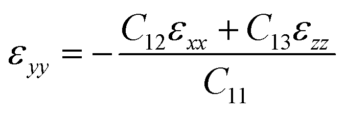 10]ZnO//[00]LGO direction, y represents the [010]ZnO//[100]LGO direction and z represents the [0001]ZnO//[001]LGO direction. The elastic stiffness coefficient Cij is taken from ref. 42. The measured εzz of −0.5% is low compared to the fully strained value of 3.8%, indicating that the misfit strain in [0001]ZnO direction is almost relaxed. The strain εxx is calculated as −0.8% from the measured εyy and εzz, which is 40% of the fully strained value of 2.0%. A lower strain residual in the [0001]ZnO direction is reasonable because the accumulated strain reaches the critical value much faster than that in its orthogonal direction.
 | ||
| Fig. 3 Reciprocal space maps of the (a) (200) and (b) (201) reflections of the ZnO epilayer. | ||
The QWs sample exhibits a similar RSM feature of no tilt of the layers as shown in Fig. 4a. However, only a small portion of the strain is relaxed along [0001]ZnO as shown in Fig. 4b. The in-plane strain in [0001]ZnO direction is −2.3%, but is as low as 0.3% in [110]ZnO direction. In other words, the strain in the low-mismatch direction (i.e., [110]ZnO) is relaxed completely, whereas two third of the strain in [0001]ZnO direction is not relaxed yet. Table 1 summarizes the strain values calculated and measured in three crystallographic directions. The unusual strain relaxation along [110]ZnO of the ZnO layer in the QWs sample may be attributed to the deposition of the Zn0.55Mg0.45O layer. First, the lattice strains at the growth temperature of 700 °C are lower than those at room temperature as a result of the large TECs of the LGO substrate (see Table 1). Second, TEM observations confirm that the thickness of the ZnO layer is as low as 30 nm, which is close to its critical thickness of strain relaxation. Consequently, the ZnO layer should remain in a state of nearly fully strained. The alloying of 45% of Mg in ZnO causes a dilation of the a axis from 0.3250 to 0.3270 nm but a shrinkage of the c axis from 0.5207 to 0.5146 nm.37 The deposition of the Zn0.55Mg0.45O layer accordingly applies an additional compressive stress on the ZnO layer underneath which inhibits the relaxation of strain. However, the tensile stress introduced by the Zn0.55Mg0.45O layer along the [110]ZnO direction indeed accelerates the strain relaxation. A schematic sketch is given in Fig. 5 to explain the unusual strain relaxation phenomenon. Moreover, we argue that the anisotropic strain relaxation is responsible for the formation of the stripes revealed in Fig. 1. The stripes grow along the direction in which the lattice strain is relaxed. The anisotropy of the rocking-curve FWHM may also be related to the anisotropic strain relaxation for which further studies are needed.
 | ||
| Fig. 4 Reciprocal space maps of the (a) (200) and (b) (201) reflections of the ZnO/Zn0.55Mg0.45O QWs. | ||
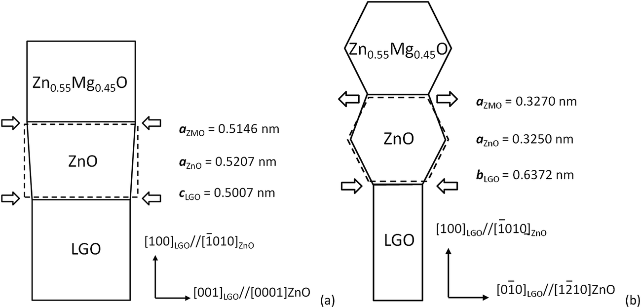 | ||
| Fig. 5 Schematic sketch showing the strain relaxation of the embedded ZnO layer in the QWs sample in (a) [0001] direction and (b) [110] direction. | ||
3.3 Microstructure and defects
In order to evaluate the microstructure of the heteroepilayers, TEM experiments were performed to study the generated defects due to the lattice mismatch. Fig. 6 shows the cross-section TEM bright field images taken with different two-beam conditions in the [110]ZnO direction of the QWs sample. According to the g × R = n extinction rule, type I1 or I2 intrinsic basal stacking faults (BSFs) are visible in two-beam conditions at g = 100, but invisible at g = 0002. In addition, type c and a + c dislocations are visible at g = 0002 in two-beam conditions. In view of this, the dense defects observed under the condition of g = 100 in Fig. 6a consist entirely of BSFs. The BSFs extend all from the substrate/film interface to the film surface. The two beam image of g = 0002 in Fig. 6b is almost free from dislocations, indicating that the sample contains a low density of threading dislocations. In addition, the strain contrast in the Zn0.55Mg0.45O layer is less significant than that found in the ZnO layer, indicating that the mismatch strain has been accommodated mostly in the ZnO layer. Because the TDs contain no screw component, the low FWHM values of the XRD rocking curves observed for both samples coincide well with our TEM observations. The density of TDs is estimated to be 1 × 108 cm−2 or lower and that of BSFs is approximately 1 × 106 cm−1. In our sample, the BSFs are extinguished at g = 0002, whereas their related partial dislocations are in contrast excluding the possibility of type I2. In fact, type I1 BSFs are the most common planar defects in nonpolar ZnO epilayers grown on various substrates, such as r-plane as well as m-plane sapphire and (100) γ-LiAlO2.13,14,38 BSFs, mainly of I1 type, have also been one of the most frequently reported defects in m- or a-plane GaN.43–45 There are at least two mechanisms corresponding to the formation of type I1 BSFs. One origin of the BSFs is that they result from the accommodation of lattice mismatch along the c-axis by adding single (0002) extra half planes.44,46 Another mechanism suggests that the BSFs form by the coalescence of nuclei at the initial stages of the growth.43 We assume the BSF densities of three cases, m-plane ZnO grown on LGO, m-plane ZnO on γ-LiAlO2 and m-plane Zn0.8Mg0.2O on γ-LiAlO2, to be 1.5 × 106 cm−1, 2.7 × 105 cm−1 and 8.2 × 104 cm−1, respectively, if the lattice misfit along the c-axis of ZnO is completely relaxed by forming BSFs. The estimated values are slightly higher than the measured values of 1 × 106 cm−1 for the ZnO epilayer in the present study as well as of 1 × 105 cm−1 and 2–3 × 104 cm−1 for the ZnO and Zn0.8Mg0.2O on γ-LiAlO2.38 In other words, the BSFs observed in the epilayer and QWs samples are probably formed, at least to a large extent, by the relaxation mechanism. However, no BSFs originating from the ZnO/Zn0.55Mg0.45O interface have been observed, indicating that the misfit strain between these two layers along the c-axis remains in an elastic state. The strain contrast of the ZnO layer (Fig. 6b) supports this argument.
 | ||
| Fig. 6 TEM bright field images at (a) g = 100 and (b) g = 0002 in two beam conditions of the ZnO/Zn0.55Mg0.45O QWs observed along the [110] cross-section orientation. | ||
The high FWHM value of the (011) rocking curve is indeed the result of the high density of type I1 basal stacking faults. It is known that the fault can be treated as a three-layer structure having the zinc-blende symmetry. Accordingly, the distance between the close-packed planes has to be expanded toward an ideal c/a ratio of 1.63. The expansion rotates the (011) plane and causes the broadening of the reciprocal spot. The origin of BSFs may be related to the steps on the substrate surface and/or the accommodation of the ZnO/substrate lattices.14 The present study therefore demonstrates that the LiGaO2 (100) substrate is an ideal substrate for growing nonpolar ZnO epilayers and heterostructures, but further improvements of the polishing technique and surface preparation technique are needed.
High resolution TEM was also used to investigate the QW interfaces and the accurate QW width. Fig. 7a shows a high resolution image of the multiple QWs taken along the [110] zone axis. The well and barrier layers can be well resolved, due to the difference in the atomic scattering factors between Zn and Mg,47 with smooth interfaces and good periodicity. The ZnO well layers are indicated by arrows in Fig. 7a. The QW width and the barrier thickness was measured to be 1.1 and 0.6 nm, respectively. In addition, BSFs can be found and are indicated by white lines. Fig. 7b is the Fourier filtered image of the QWs which further confirms the good uniformity across the entire structure. Fig. 7c is the Fourier filtered image of the lower dashed square area in Fig. 7a, confirming that the BSF is of I1 type.
 | ||
| Fig. 7 (a) High resolution TEM image taken along the [110] zone axis with the growth direction (GD) indicated by a fine arrow, the BSFs indicated by white lines and the position of the ZnO well layers labeled by white arrows, as well as the Fourier filtered images of (b) the multiple quantum wells (upper dashed square) and (c) a basal stacking fault (lower dashed square). | ||
3.4 Cathodoluminescence
Fig. 8a shows the CL spectra of the ZnO epilayer and QWs samples recorded at room temperature with a 5 kV electron beam. A strong emission at 3.29 eV accompanied with a weak deep level emission at approximately 2.3 eV is observed for the epilayer sample. The emission peak at 3.29 eV is indeed composed of two Gaussian peaks at 3.30 eV and 3.24 eV, respectively. The former corresponds to the near band-edge emission (NBE), whereas the latter at 3.24 eV is a SF-related emission with a broad FWHM of 290 meV.48,49 The integrated intensity of the SF-related peak is slightly higher than that of the NBE peak, indicating that the density of the SFs is so high that the recombination events are mostly confined in the SFs. In fact, the basal SFs are usually treated as quantum wells with a type-II band alignment.50 A much stronger NBE consisting of at least three components is observed for the QWs sample. The incorporation of Mg in ZnO induces a blue shift of the bandgap energy to ∼4.2 eV for x = 0.45.37,51 The weak emission peak components at 4.18 eV and 3.29 eV correspond to the Zn0.55Mg0.45O layer and the ZnO layer, respectively, indicating highly efficient carrier confinement in the well regions, which is a desirable feature for laser diodes and light emitting diodes. The strong CL peak at 3.56 eV is emitted from the quantum wells and hence shows a pronounced blue shift. The shift is attributed to both the positive quantum confinement effects and the absence of the internal polarization fields. Fig. 8b shows the monochromatic CL image at 3.56 eV of the QWs sample. The emission intensity is uniformly distributed. In our previous result, BSFs were clearly resolved as dark lines in the monochromatic CL image as their density was low (2–3 × 104 cm−1). Nevertheless, these dark lines became less evident in the CL image for a sample having a higher BSF density of 1 × 105 cm−1. It is thus believed that the BSFs can no longer be resolved in the CL image of Fig. 8b when the BSF density is as high as 1 × 106 cm−1. The role of stacking faults on the optical emission in nonpolar ZnO and GaN is still under discussion. Room-temperature CL measurements showed that the ultraviolet luminescence is quenched by the presence of BSFs in ZnO nanorods grown by a hydrothermal technique.52 The CL analysis of InGaN/GaN nanodisk-in-rod heterostructures at 96 K also indicated that the quenching of the CL emission was directly correlated to the presence of SFs inside the InGaN nanodisks.53 However, an emission at about 50 meV lower than the energy of the donor-bound exciton emission was observed in a CL spectrum acquired at 7 K from a ZnO epilayer grown on LiAlO2. This emission was assigned to luminescence associated with type I1 BSFs. It was argued that the BSF emission was not quenched but became very broad at room temperature.48 Accordingly, the low-energy tail of the NBE luminescence of the epilayer sample is assigned to a BSF-related emission as shown in the inset of Fig. 8a. | ||
| Fig. 8 (a) CL spectra of the ZnO epilayer and ZnO/Zn0.55Mg0.45O QWs measured at room temperature with 5 kV electron beam and (b) the monochromatic image of the QWs sample at 3.56 eV. The inset in (a) shows the deconvolution result of the NBE peak for the epilayer sample. | ||
For comparison, we have determined the transition energy of the excitons confined in the quantum wells by using a variation model.3,54 The following parameters were used for the numerical calculation: me = 0.28m0, mhh = 0.95m0 and mlh = 059m0 for the electron, heavy hole and light hole effective mass, respectively, 3.75 for the dielectric constant, bandgap offset ΔEg = 0.91 eV, and a conduction band to valence band offset ratio of 50/50.1,3 The exciton transition energy of our 5-period ZnO/Zn0.55Mg0.45O QWs was calculated to be 3.55 eV, which is in very good agreement with the experimental data.
4. Conclusion
Nonpolar m-plane ZnO epilayers and ZnO/Zn0.55Mg0.45O multiple quantum wells have been grown successfully on LiGaO2 (100) substrate by plasma-assisted molecular beam epitaxy. The epilayer and QWs samples show different anisotropy of the X-ray rocking curves (RCs) and the surface stripes. The former exhibits a low FWHM value of 126 arcsec of the X-ray (100) RC along [110]ZnO, and its surface is composed of fine stripes along [0001]ZnO. The QWs sample, however, exhibits a low RC FWHM along [0001]ZnO with surface stripes oriented along [110]ZnO. The differences of stripe orientation and RC FWHM can be attributed to the anisotropic stress relaxation. Combining the X-ray and TEM characterization techniques, both samples show an extremely low density of threading dislocations of less than 1 × 108 cm−2, but a high density of basal stacking faults of 1 × 106 cm−1. Room-temperature CL measurement have confirmed that the 5-period ZnO (1.1 nm)/Zn0.55Mg0.45O (0.6 nm) multiple quantum wells exhibit a strong emission at 3.56 eV, resulting from the positive quantum confinement effects and the absence of internal polarization fields.
Acknowledgements
This work is financially supported by the National Science Council of Taiwan under grant no. NSC100-2221-E-110-055-MY3, by the Aim for the Top University Project as well as the Center for Nanoscience and Nanotechnology, National Sun Yat-Sen University.References
- Ü. Özgür, Ya. I. Alivov, C. Liu, A. Teke, M. A. Reshchikov, S. Doğan, V. Avrutin, S.-J. Cho and H. Morkoç, J. Appl. Phys., 2005, 98, 041301 CrossRef.
- S. F. Varol, D. Şahin, M. Kompisas and G. Çankaya, RSC Adv., 2014, 4, 13593 RSC.
- G. Coli and K. K. Bajaj, Appl. Phys. Lett., 2001, 78, 2861 CrossRef CAS.
- T. Makino, Y. Segawa, M. Kawasaki and H. Koinuma, Semicond. Sci. Technol., 2005, 20, S78 CrossRef CAS.
- A. Dal Corso, M. Posternak, R. Resta and A. Baldereschi, Phys. Rev. B: Condens. Matter Mater. Phys., 1994, 50, 10715 CrossRef CAS.
- C. Morhain, T. Bretagnon, P. Lefebvre, X. Tang, P. Valvin, T. Guillet, B. Gil, T. Taliercio, M. Teisseire-Doninelli, B. Vinter and C. Deparis, Phys. Rev. B: Condens. Matter Mater. Phys., 2005, 72, 241305 CrossRef.
- P. Waltereit, O. Brandt, A. Trampert, H. T. Grahn, J. Menniger, M. Ramsteiner, M. Reiche and K. H. Ploog, Nature, 2000, 406, 865 CrossRef CAS PubMed.
- W. L. Wang, Y. H. Lin, W. J. Yang, Z. L. Liu, S. Z. Zhiou, H. R. Qian, F. Q. Gao, L. Wen and G. Q. Li, J. Mater. Chem. C, 2014, 2, 4112 RSC.
- S. H. Park, T. Minegishi, H. J. Lee, D. C. Oh, H. J. Ko, J. H. Chang and T. Yao, J. Appl. Phys., 2011, 110, 053520 CrossRef.
- H. Shen, C. X. Shan, Q. Qiao, J. S. Liu, B. H. Li and D. Z. Shen, J. Mater. Chem. C, 2013, 1, 234 RSC.
- J. Zippel, M. Lorenz, M. Lange, M. Stölzel, G. Benndorf and M. Grundmann, J. Cryst. Growth, 2013, 364, 81 CrossRef CAS.
- J.-M. Chauveau, M. Teisseire, H. Kim-Chauveau, C. Deparis, C. Morhain and B. Vinter, Appl. Phys. Lett., 2010, 97, 081903 CrossRef.
- P. Vennéguès, J.-M. Chauveau, M. Korytov, C. Deparis, J. Zuniga-Perez and C. Morhain, J. Appl. Phys., 2008, 103, 083525 CrossRef.
- S. K. Han, J.-H. Kim, J. W. Lee, J. G. Kim, M. Jeong, J. Y. Lee, S. I. Hong, J. S. Park, Y. E. Ihm, J.-S. Ha and T. Yao, Thin Solid Films, 2011, 519, 6394 CrossRef CAS.
- H. Song, J.-H. Kim, E. K. Kim and S.-M. Hwang, Thin Solid Films, 2009, 517, 3927 CrossRef CAS.
- Y. Li, Y. Zhang, H. He, Z. Ye, J. Jiang, J. Lu and J. Huang, Mater. Res. Bull., 2012, 47, 2235 CrossRef CAS.
- J.-M. Chauveau, D. A. Buell, M. Laügt, P. Vennéguès, M. Teisseire-Doninelli, S. Berard-Bergery, C. Deparis, B. Lo, B. Vinter and C. Morhain, J. Cryst. Growth, 2007, 301–302, 366 CrossRef CAS.
- Y. Li, X. H. Pan, Y. Z. Zhang, H. P. He, J. Jiang, J. Y. Huang, C. L. Ye and Z. Z. Ye, J. Appl. Phys., 2012, 112, 103519 CrossRef.
- S. Choopun, R. D. Vispute, W. Yang, R. P. Sharma, T. Venkatesan and H. Shen, Appl. Phys. Lett., 2002, 80, 1529 CrossRef CAS.
- S. K. Han, H. S. Lee, D.-Y. Kim, S.-K. Hong, B. J. Ahn, J.-H. Song, M. Jeong, J. H. Lee and T. Yao, J. Alloys Compd., 2015, 623, 1 CrossRef CAS.
- G. Q. Li, S.-J. Shih and Z. Y. Fu, Chem. Commun., 2010, 46, 1206 RSC.
- W. J. Yang, W. L. Wang, Z. L. Liu, Y. H. Lin, S. Z. Zhou, H. R. Qian and G. Q. Li, CrystEngComm, 2015, 17, 1073 RSC.
- R. Schuber, M. M. C. Chou and D. M. Schaadt, Thin Solid Films, 2010, 518, 6773 CrossRef CAS.
- W. L. Wang, W. J. Yang, H. Y. Wang and G. Q. Li, J. Mater. Chem. C, 2014, 2, 9342 RSC.
- M. M. C. Chou, C. L. Chen, D. R. Hang and W.-T. Yang, Thin Solid Films, 2011, 519, 5066 CrossRef CAS.
- W. J. Yang, W. L. Wang, Y. H. Lin, Z. L. Liu, S. Z. Zhou, H. R. Qian, F. L. Gao, S. G. Zhang and G. Q. Li, J. Mater. Chem. C, 2014, 2, 801 RSC.
- G. Q. Li, W. L. Wang, W. J. Yang and H. Y. Wang, Surf. Sci. Rep., 2015, 70, 380 CrossRef CAS.
- T. Huang, S. Zhou, H. Teng, H. Lin, J. Wang, P. Han and R. Zhang, J. Cryst. Growth, 2008, 310, 3144 CrossRef CAS.
- M. M. C. Chou, D.-R. Hang, C. L. Chen and Y.-H. Liao, Thin Solid Films, 2011, 519, 3627 CrossRef CAS.
- J.-Y. Yu, T.-H. Huang, L. Chang, Y.-H. Liao, M. M. C. Chou and D. Gan, J. Electrochem. Soc., 2011, 158, 1166 CrossRef.
- C.-Y. Lee, C. L. Chen, L. Chang and M. M. C. Chou, J. Cryst. Growth, 2014, 407, 11 CrossRef CAS.
- D.-R. Hang, S. E. Islam, K. H. Sharma, C. L. Chen, C.-T. Liang and M. M. C. Chou, Semicond. Sci. Technol., 2014, 29, 085004 CrossRef.
- J. E. Ayers, Heteroepitaxy of Semiconductors: theory, growth, and characterization, CRC press, 2007 Search PubMed.
- M. Marezio, Acta Crystallogr., 1965, 18, 481 CrossRef CAS.
- C. J. Rawn and J. Chaudhuri, J. Cryst. Growth, 2001, 225, 214 CrossRef CAS.
- H. Iwanaga, A. Kunishige and S. Takeuchi, J. Mater. Sci., 2000, 35, 2451 CrossRef CAS.
- A. Ohtomo, M. Kawasaki, T. Koida, K. Masubuchi, H. Koinuma, Y. Sakurai, Y. Yoshida, T. Yasuda and Y. Segawa, Appl. Phys. Lett., 1998, 72, 2466 CrossRef CAS.
- T.-H. Huang, W.-H. Lin, T. Yan, J.-J. Wu, L. Chang, M. M. C. Chou, U. Jahn and K. H. Ploog, ECS J. Solid State Sci. Technol., 2013, 2, 338 CrossRef.
- J.-M. Chauveau, J. Vives, J. Zuniga-Perez, M. Laugt, M. Teisseire, C. Deparis, C. Morhain and B. Vinter, Appl. Phys. Lett., 2008, 93, 231911 CrossRef.
- S. K. Han, S. K. Hong, J. W. Lee, J. Y. Lee, J. H. Song, Y. S. Nam, S. K. Chang, T. Minegishi and T. Yao, J. Cryst. Growth, 2007, 309, 121 CrossRef CAS.
- B. Heying, X. H. Wu, S. Keller, Y. Li, D. Kapolnek, B. P. Keller, S. P. DenBaars and J. S. Speck, Appl. Phys. Lett., 1996, 68, 643 CrossRef CAS.
- New Series, Group III: Solid State Physics, Low Frequency Properties of Dielectric Crystals: Elastic Constants, ed. O. Madelung Landolt-Börnstein, Springer, Berlin, 1993, vol. 29a Search PubMed.
- P. Vennéguès, J. M. Chauveau, Z. Bougrioua, T. Zhu, D. Martin and N. Grandjean, J. Appl. Phys., 2012, 112, 113518 CrossRef.
- A. Lotsari, Th. Kehagias, G. Tsiakatouras, K. Tsagaraki, M. Katsikini, J. Arvanitidis, D. Christofilos, S. Ves, Ph. Komninou, A. Georgakilas and G. P. Dimitrakopulos, J. Appl. Phys., 2014, 115, 213506 CrossRef.
- C.-H. Shih, T.-H. Huang, R. Schuber, Y.-L. Chen, L. Chang, I. Lo, M. M. C. Chou and D. M. Schaadt, Nanoscale Res. Lett., 2011, 6, 425 CrossRef PubMed.
- J. Smalc-Koziorowska, G. Tsiakatouras, A. Lotsari, A. Georgakilas and G. P. Dimitrakopulos, J. Appl. Phys., 2010, 107, 073525 CrossRef.
- P. Hirsch, A. Howie, R. B. Nicholson, D. W. Pashley and M. J. Whelan, Electron Microscopy of thin crystal, Robert E. Krieger Publishing Co. Inc., 1st edn, 1965 Search PubMed.
- W.-H. Lin, U. Jahn, H. T. Grahn, L. Chang, M. M. C. Chou and J.-J. Wu, Appl. Phys. Express, 2013, 6, 061101 CrossRef.
- D. Das and P. Mondal, RSC Adv., 2014, 4, 35735 RSC.
- Y. Yan, G. M. Dalpian, M. M. Al-Jassim and S.-H. Wei, Phys. Rev. B: Condens. Matter Mater. Phys., 2004, 70, 193206 CrossRef.
- T. Takagi, H. Tanaka, S. Fujita and S. Fujita, Jpn. J. Appl. Phys., 2003, 42, L401 CrossRef CAS.
- B. Sieber, A. Addad, S. Szunerits and R. Boukherroub, J. Phys. Chem. Lett., 2010, 1, 3033 CrossRef CAS.
- X. Zhou, M.-Y. Lu, Y.-J. Lu, E. J. Jones, S. Gwo and S. Gradečak, ACS Nano, 2015, 9, 2868 CrossRef CAS PubMed.
- P. Bigenwald, P. Lefebvre, T. Bretagnon and G. Bil, Phys. Status Solidi B, 1999, 216, 371 CrossRef CAS.
| This journal is © The Royal Society of Chemistry 2015 |