
Presence of metal-oxide interface enhanced photoluminescence from In–In2O3 core–shell nanorods
Kavita Yadav,
B. R. Mehta and
J. P. Singh*
Department of Physics, Indian Institute of Technology Delhi, Hauz Khas, New Delhi-110016, India. E-mail: jpsingh@physics.iitd.ac.in
First published on 24th November 2014
Abstract
The photoluminescence (PL) properties of indium oxide (IO) and In–In2O3 core–shell nanorods have been studied at different temperatures in order to understand the role of metal-oxide interfaces and defects on PL emission. The GAXRD spectra confirm the presence of In phase in the core–shell nanorods and STEM-EDX results show that the core of the nanorods is filled with In metal. The Raman and STEM-EDX results show that the core–shell nanorods are more oxygen deficient and indium-rich as compared to IO nanorods. Further comparison of the two samples shows that In–In2O3 core–shell nanorods have relatively intense PL emission, large increase in PL intensity with decreasing sample temperature, and the observation of a near band edge emission. This is due to the presence of an In-rich and oxygen deficient In–In2O3 interface and the passivation of defects because of the presence of hydrogen during the synthesis of the IO core–shell nanorods. The enhanced PL emission in the core–shell nanorods may have potential applications in future optoelectronics.
1. Introduction
Indium oxide (IO), a wide band gap (∼3.6 eV) semiconductor having good electrical conductivity and high optical transparency, is a promising material for electronic and optoelectronic devices. A strong photoluminescence (PL) in ultraviolet and visible ranges were observed in IO nanostructures with different morphologies at room temperature.1–6 The researchers have reported PL peaks at 416, 435 and 470 nm for IO nanowires,1,2 at 429 nm for ordered IO nanowires embedded in anodic alumina membranes,3 at 470 nm for IO nanopyramids and nanocoloumns,4 at 670 nm for IO nanowires,5 and at 637 nm for IO thin film.6 Previous studies mainly focused on the PL emission from IO nanowires, thin films and octahedra. An investigation on IO core–shell nanostructures is still lacking. It is well known that optoelectronic properties of core–shell structures get modified due to the presence of interfaces and also due to changes at the nanostructure surface with capping by the shell layer.7,8 The properties of these nanostructures are dependent on the diameter of the core and thickness of shell.9–11In this paper, the central objective is to investigate the role of defects and the presence of metal-oxide interface on the PL properties of IO core–shell nanorods. The temperature dependent PL properties of IO nanorods and core–shell IO nanorods reveals important information about the nature of defects states contributing towards the PL emission.
2. Experimental details
The core–shell IO nanorods (sample A) were synthesized using a horizontal tube furnace at a temperature of 1000 °C and one atmospheric pressure. An alumina boat with In2O3 + C (1![[thin space (1/6-em)]](https://www.rsc.org/images/entities/char_2009.gif) :1) powder mixture was placed at the centre of the tube furnace and a gold coated Si (∼5 nm) substrate was placed downstream at a temperature of 960 °C. The carrier gas Ar, with a constant flow of 200 sccm, was bubbled through a hot ethanol pot (∼65 °C) and then flowed into the quartz tube so that ethanol vapors were continuously carried into the reaction zone. The reaction was carried out under reducing ambient for 1 hour. The IO nanorods (sample B) were also synthesized for the comparative analysis. The growth of IO nanorods on sample B was carried out under pure Ar gas with a constant flow rate of 200 sccm for 1 hour.
:1) powder mixture was placed at the centre of the tube furnace and a gold coated Si (∼5 nm) substrate was placed downstream at a temperature of 960 °C. The carrier gas Ar, with a constant flow of 200 sccm, was bubbled through a hot ethanol pot (∼65 °C) and then flowed into the quartz tube so that ethanol vapors were continuously carried into the reaction zone. The reaction was carried out under reducing ambient for 1 hour. The IO nanorods (sample B) were also synthesized for the comparative analysis. The growth of IO nanorods on sample B was carried out under pure Ar gas with a constant flow rate of 200 sccm for 1 hour.
The as-synthesized nanostructures were characterized by glancing angle X-ray diffraction (GAXRD) using Phillips X'Pert, PRO-PW 3040 diffractometer with a thin film attachment, field emission scanning electron microscope (FESEM) (FEI Quanta 3D FEG) and high resolution transmission electron microscope (HRTEM) (Tecnai G20-Stwin at 200K). Scanning transmission electron microscope (STEM) with energy dispersive X-ray (EDX) facility was used to determine the position dependent stoichiometry of the IO nanorods. The PL measurements were performed on Renishaw inVia micro-Raman system equipped with closed cycle cryostat (Oxford instruments). The PL spectra were recorded for both samples at different sample temperatures ranging from 300 K to 10 K, while a He–Cd laser with an excitation source wavelength of 325 nm was used. The measurement conditions were kept identical for both of the samples. Raman spectroscopy of IO nanorods was carried out using a Renishaw micro-Raman setup having a Renishaw's RenCam CCD detector; an Ar ion laser with an excitation wavelength of 514 nm was used for Raman measurements. The electron paramagnetic resonance (EPR) spectroscopy measurements were recorded on a continuous wave X-band Elexsys 580 EPR spectrometer (Bruker Biospin Corporation) operating at a frequency of 9.64 GHz. The IO nanorods and nanorods samples were purged with Ar gas prior to the EPR measurements. The spectra were acquired at the microwave power of 3.13 mW, modulation frequency of 100 kHz and the modulation amplitude value of 1G. The line shape of the EPR spectra of IO nanostructures was simulated using Easyspin simulation program.12
3. Results and discussions
The GAXRD spectra of the two types of IO nanostructured samples are shown in Fig. 1. The GAXRD spectrum of sample A shows two peaks at 2θ = 33.1° (101) and at 39.2° (110) corresponding to a structure of In along with indium oxide peaks which confirms the presence of In in the sample A nanostructures. The intense peaks in GAXRD spectra of sample B are well indexed to cubic In2O3 with a lattice constant of 1.011 nm and no peak corresponding to In was observed.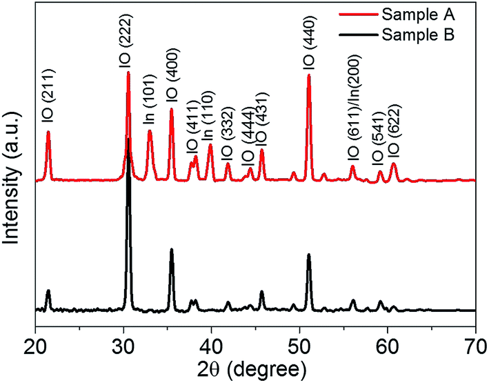 | ||
| Fig. 1 GAXRD spectra of samples A and B synthesized by chemical vapour deposition method. The XRD spectra contributed only from IO nanostructures, as the patterns were collected with 1° glancing angle. | ||
Fig. 2(a) and (b) show the FESEM images of samples A and B. The IO core–shell nanorods (later confirmed by TEM) on sample A are 26 ± 8 μm long with a diameter of 107 ± 12 nm. The average length and diameter of IO nanorods on sample B were observed to be 21 ± 5 μm and 120 ± 31 nm, respectively. The HRTEM micrographs show the crystalline nature of IO nanostructures. The average core and shell thickness of IO core–shell nanorods were found to be 75 nm and 18 nm, respectively. The lattice fringe spacing of 0.506 nm corresponds to (200) plane and reveals that core–shell IO nanorods grow along the 〈100〉 direction as shown in Fig. 2(c). The IO nanorods on sample B have lattice fringe spacing of 0.292 nm which corresponds to the (222) plane of cubic IO as shown in Fig. 2(d). To investigate the qualitative difference in the stoichiometry of IO nanostructures on samples A and B, STEM-EDX measurements were performed on a single IO nanorod at three different positions along the diameter.
 | ||
| Fig. 2 FESEM images of (a) sample A and (b) sample B. (c) HRTEM micrograph of core–shell IO nanorods (sample A) with growth direction along 〈100〉. (d) HRTEM micrograph of IO nanorods (sample B). The insets represents the TEM micrograph of IO nanostructures. | ||
For sample A, the In:O ratio at point 1 and 3 (shell of nanorod) (shown in inset of Fig. 2(c)) is 43:57 and 41:59, respectively. The In:O ratio at point 2 (core of nanorod) is 60:40. The STEM-EDX results clearly show that the core of the IO nanorod on sample A is filled with In metal. The oxygen content observed in the core is due to the background signals and the presence of the shell around the core. The average In:O ratio of IO nanorods on sample B at three different points, as indicated in the inset of Fig. 2(d) is 39:61.
The reaction ambient play an important role during synthesis of IO nanostructures with different morphology in CVD process. It was observed that for conventional growth of IO nanostructures using gold as catalyst and Ar as carrier gas resulted into the formation of IO nanorods. The growth of IO nanorods is well explained by using vapor–liquid–solid (VLS)13 and vapor–solid–solid (VSS)14 growth mechanism in the literature. Here, the growth took place via VLS mechanism. The gold catalyst acts as preferential absorbing site for incoming IO vapour species. The growth is governed by the metal catalyst at the growth front and results in formation of nanorods. Whereas, the IO core–shell nanorods grow in presence of ethanol which act as reducing reagent. Ethanol reduces IO into In-rich reactive species during growth. Indium forms In–Au liquid alloy which acts as initial nuclei for the growth of nanorods. As growth continues the excess In may get phase separated from In2O3 and encapsulated inside as core. The effect of ethanol ambient on the core–shell morphology have been reported in our earlier published work.15,16
PL studies were carried out on IO core–shell nanorods and IO nanorods in order to study the effects of a thin IO shell (∼18 nm) and the presence of In–In2O3 core–shell structure on PL emission. Room temperature PL emission spectra from samples A and B are shown in Fig. 3(a). The PL emission from IO nanorods on sample B is very weak but an intense PL emission is observed from core–shell IO nanorods on sample A. Since the broad PL band is asymmetrical, it can be inferred that the PL band should have more than one origin. The PL band consists of several contributions originating from different defects. The broad emission can be deconvoluted into three peaks by using multiple Gaussian peaks fitting. The three peaks are centered at wavelength of 610 nm (orange), 721 nm (red) and 850 nm (Infra-red (IR)). The intensity of PL emission from sample A was found to be about 10 times higher than that of sample B at room temperature. The difference in the luminescence intensities is related to the difference in nature and concentration of surface defects in the two cases. The presence of In–In2O3 interface in IO core–shell nanorods makes the stoichiometry of IO nanorods more oxygen-deficient and In-rich. In sample A, PL signal is mainly due to the presence of an interface and nanosized IO shell as the In core is not expected to have emission. Due to the nanoscale thickness of the shell (∼18 nm) of IO nanorods in sample A as compared to 120 ± 31 nm diameter of IO nanorods in sample B, the defect concentration is expected to be much higher in sample A. The intense PL emission observed from these core–shell nanorods at room temperature is thus related to the presence of a metal oxide interface and nanoscale thickness of IO shell. The higher PL emission corresponding to deep level defects for ZnO nanowires with higher aspect ratio is also reported in the literature.17,18
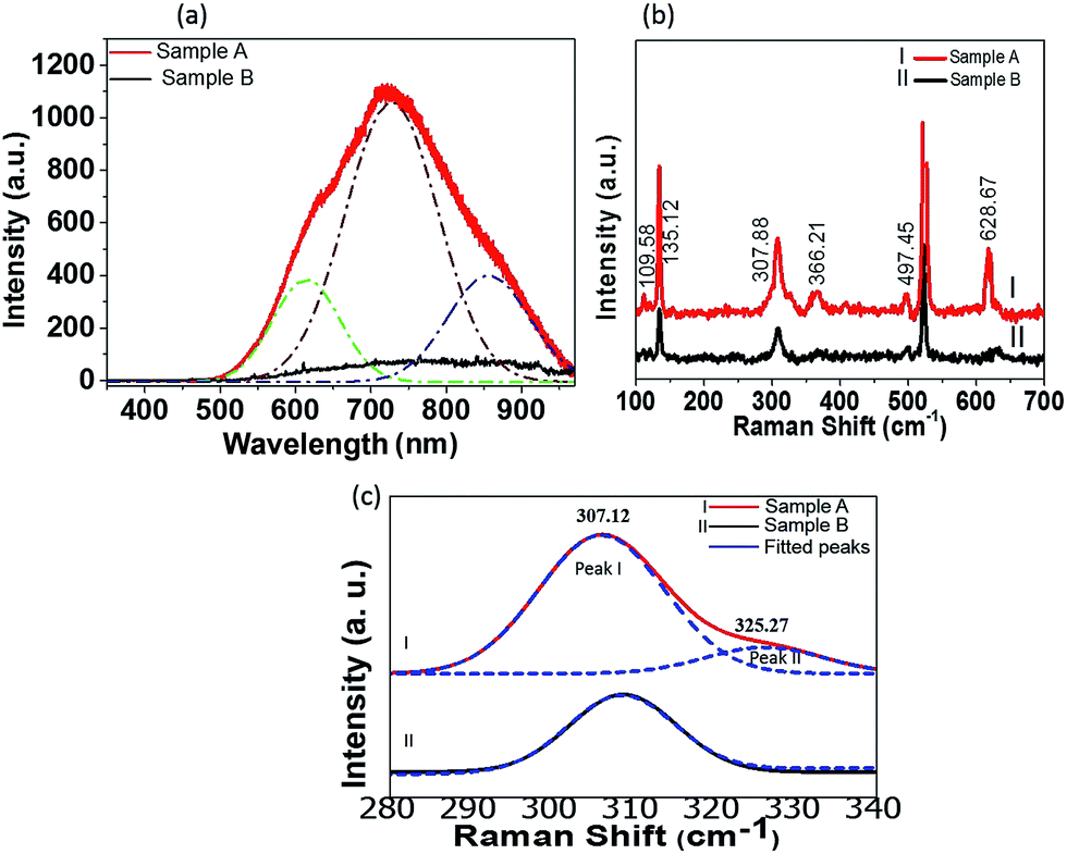 | ||
| Fig. 3 (a) Room temperature PL spectra of samples A and B. (b) Raman spectra of samples A and B and (c) the multiple Gaussian peaks fit for 307.88 cm−1 peak for sample A and B. | ||
As shown in Fig. 3(b), the Raman spectra of samples A and B exhibit peaks at 109.58, 135.12, 307.88, 366.21, 497.45 and 628.67 cm−1. The Raman peak observed at 307.88 cm−1 was found to be symmetric in sample B whereas it is asymmetric in sample A. The asymmetric peak in sample A is deconvoluted into two separate peaks at 307.12 cm−1 and 325.27 cm−1 as shown in Fig. 3(c). The asymmetry in the Raman peak can be ascribed to the quantum confinement effect19 or nonstoichiometry20 in nanostructures. Due to a relatively larger diameter of IO nanorods (120 ± 31 nm) and shell thickness (∼18 nm) of core–shell nanorods, any significant quantum confinement effects can be ruled out. Parker and Siegel21 have reported that changes in Raman peak i.e. line shift and peak broadening can be used for a quantitative assessment of the stoichiometry of nanophase materials. The Raman peak at 307.88 cm−1 corresponds to the stretching mode of IO and is sensitive to the presence of oxygen vacancies.22,23 In the present study, the Raman and STEM-EDX analysis confirm that the IO core–shell nanorods in sample A are more oxygen-deficient as compared to the IO nanorods in sample B. The room temperature PL intensity (at room temperature) is significantly higher in core–shell IO nanorods, having larger number of oxygen vacancies and indium interstitial defects in comparison to the IO nanorods. It leads to be an indication of the possible role of oxygen vacancies and indium interstitial defects for the observed PL emission at room temperature. EPR measurements were done on both of the samples as shown in Fig. 4. EPR peak at 3445.6 G indicate a g value of 2.0025, which is in agreement with the g value reported for the singly ionised oxygen vacancy (V+) defects in IO.4,23
 | ||
| Fig. 4 EPR spectra measured from core–shell IO nanorods (sample A) and IO nanorods (sample B). | ||
The nearly same EPR signal or singly ionised oxygen vacancies (V+) for both of the samples and about 10 times larger room temperature PL emission from IO core–shell nanorods as compared to IO nanorods suggest that the singly ionised oxygen vacancies are not related to the PL from IO core–shell nanorods.
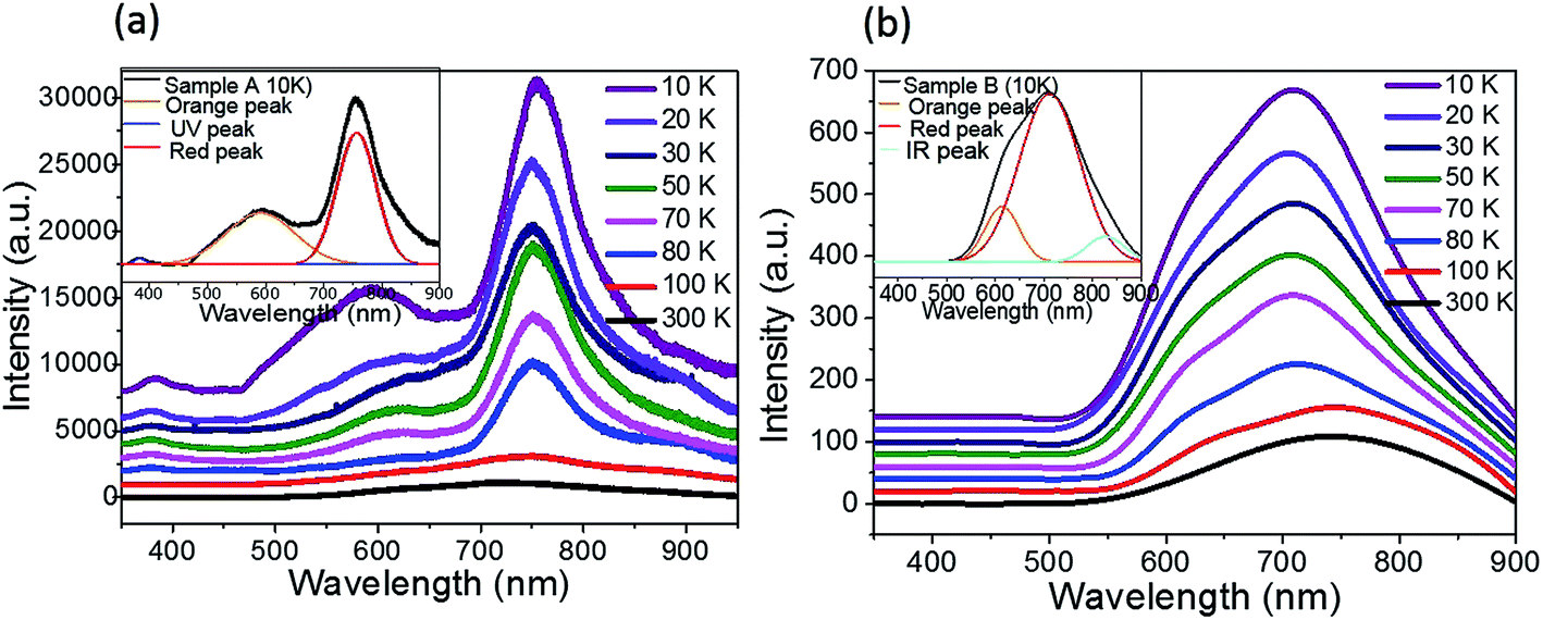
To further investigate the nature of defects states contributing towards PL emission, temperature dependent PL measurements were carried out for sample A and B, where sample temperature was varied from 300 K to 10 K as shown in Fig. 5. In the core–shell IO nanorods (sample A), it was observed that the broad PL signal at 300 K appears as emission peaks centred at wavelength of 590 nm (orange), 750 nm (red) and 382 nm (ultra-violet (UV)) at 10 K as shown in the inset of Fig. 5(a). Also a large enhancement of about 21 times in red PL intensity was observed at 10 K with respect to the room temperature (300 K) PL intensity. In order to study the temperature dependence on the intensity of respective emission peaks for samples A, multiple Gaussian peaks fitting was applied to all PL spectra measured at different temperatures. The two emission peaks orange and UV show blue shift with a decrease in sample temperature. The blue shift of emission peaks with decrease in sample temperature is due to the variation in the band gap with temperature.24
 | ||
| Fig. 5 Temperature dependent PL spectra of (a) sample A and (b) sample B with sample temperature varying from 300 K to 10 K. Insets show the multiple Gaussian peaks fit of PL spectra at 10 K for both the samples. | ||
The activation energies (Ea) were obtained from the slopes of an Arrhenius plot as shown in Fig. 6, where Io denotes the integrated PL intensity at 10 K and I is the integrated PL intensity at different temperatures. The obtained Ea values corresponding to orange, red and UV emission are 6.3 meV, 8 meV and 16.7 meV, respectively.
 | ||
| Fig. 6 Arrhenius plot showing the integrated PL intensities of red, orange and UV peaks of IO nanostructures versus the reciprocal sample temperature. The activation energy was derived from the slope of a straight line fit. | ||
In comparison to sample A, the red PL intensity of IO nanorods (sample B) shows only a small increase of about 5 times at 10 K with respect to the room temperature (300 K) PL intensity. The three deconvoluted peaks centred at wavelengths of 610 nm (orange), 712 nm (red) and 830 nm (Infra-red (IR)) at 10 K are shown in the inset of Fig. 5(b). The IR peak does not show significant changes with a decrease in sample temperature. The two emission peaks orange and red in sample B show blue shift with a decrease in sample temperature. The obtained Ea values corresponding to orange and red peaks are 6.3 meV and 13.6 meV, respectively as shown in Fig. 6.
The orange PL intensity of IO nanorods showed enhancement of about 11.5 times and IO core–shell nanorods showed enhancement of about 12.3 times at 10 K with respect to the room temperature (300 K) PL intensity. The enhancement observed for orange emission was nearly the same for both the samples. Also, the Ea values corresponding to the orange emission for the two samples are the same as 6.3 meV which indicates that similar types of defects are responsible for the observed orange emission from the two samples. The defect level for orange emission in our case is 590 nm (2.1 eV) and 610 nm (2.0 eV) which is in close agreement with the defect level energy reported for deep In interstitial defects at a-site (Ini_a).25 The orange emission is attributed to indium interstitial defects (Ini) present in the IO nanostructures as reported in the literature.23 The Ea value for red emission is larger for IO nanorods, (13.6 meV) as compared to the IO core–shell nanorods (8 meV). Also, as we have mentioned earlier that the enhancement in red PL intensity at 10 K was about 5 times in IO nanorods samples but in IO core–shell nanorods it was about 21 times, when measured with respect to PL intensity at 300 K. The large difference in enhancement in red PL intensity with a decrease in sample temperature and the different Ea value for red emission for the two samples suggest that the different types of defects are responsible for the red emission from IO core–shell nanorods (at 750 nm) and IO nanorods (at 712 nm). The red PL emission from the two samples is well explained on the basis of a defect level diagram proposed by Tomita et al.25 The red emission from indium oxide nanorods is observed from deep In interstitial defects at c-site (Ini_c) and the red emission from core–shell IO nanorods is observed from oxygen vacancy and indium interstitial complex deep level defects (V0–Ini). The V0–Ini complex formed when V0 and Ini positioned at a distance of about 8 Å.25 Due to the presence of a metal-oxide interface in core–shell nanorods, oxygen vacancies and indium interstitial defects concentration is higher near the interface and possibility of the formation of complex defects is more. Hence intense PL emission (750 nm) was observed from core–shell IO nanorods.
The UV emission observed in core–shell IO nanorods at 382 nm is due to the near band edge emission and depends on their crystalline quality. The core–shell IO nanorods were synthesized in the presence of ethanol ambient which acts as a source of hydrogen. The increase in excitonic luminescence is caused by the passivation of deep level defects by hydrogen. The UV enhancement with hydrogenation in ZnO was earlier reported by the researchers.26–28 The absence of UV emission in the IO nanorods sample suggests that there may exists more non-radiative recombination channels which quench the UV emission.
Tomita et al.25 studied the various point defects in In2O3 using the first principles molecular orbital calculation and reported the shallow and deep donor defect levels in In2O3. In present report, the near band edge emission (UV) is originated from shallow defects whereas orange and red emissions are originated from deep level defects as shown in Fig. 7. The analytical results presents in this study may benefit the understanding on emission properties of IO nanostructures.
 | ||
| Fig. 7 Schematic bandgap diagram showing the defect energy levels and their ionization energies (eV) of IO (ref. 25). | ||
4. Conclusions
This study shows that the PL properties of In–In2O3 core–shell IO nanorods are significantly influenced by the presence of the In–In2O3 interface. The IO core–shell nanorods exhibit intense and large PL intensity in comparison to IO nanorods at room temperature. The orange emission observed from core–shell IO nanorods (at 590 nm) and IO nanorods (at 610 nm) have 6.3 meV activation energy in both the cases and attributed to the indium interstitial (Ini_a) defects. The observed results suggest that the red emission from the two samples are obtained from different type of defects. In IO core–shell nanorods the PL emission (750 nm) is attributed to the complex defects of oxygen vacancy and In interstitial (V0–Ini), whereas in IO nanorods (712 nm) it is attributed to In interstitial (Ini_c) defects. In conclusion, the present research work suggests that the presence of an interface in core–shell nanostructures increase the complex defect concentration and enhance the PL emission.Acknowledgements
KY is thankful to the Council of Scientific and Industrial Research (CSIR), India for providing senior research fellowship. The technical support of Centre of Material Science and Engineering, NIT Hamirpur and Nanoscale Research Facility, IIT Delhi are highly acknowledged. We sincerely acknowledge Taylor Wilkinson, Metallurgical and Materials Engineering, Colorado School of Mines, Golden, Colorado for proof reading of the manuscript. This research was funded by DST, India grant numbers SR/S2/CMP-13/2010.References
- X. C. Wu, J. M. Hong, Z. J. Han and Y. R. Tao, Chem. Phys. Lett., 2003, 373, 28 CrossRef CAS.
- X. S. Peng, G. W. Meng, J. Zhang, X. F. Wang, Y. W. Wang, C. Z. Wang and L. D. Zhang, J. Mater. Chem., 2002, 12, 1602 RSC.
- M. J. Zheng, L. D. Zhang, G. H. Li, X. Y. Zhang and X. F. Wang, Appl. Phys. Lett., 2001, 79, 839 CrossRef CAS PubMed.
- P. Guha, S. Kar and S. Chaudhuri, Appl. Phys. Lett., 2004, 85, 3851 CrossRef CAS PubMed.
- G. Wang, J. Park, D. Wexler, M. S. Park and J. H. Ahn, Inorg. Chem., 2007, 46, 4778 CrossRef CAS PubMed.
- M.-S. Lee, W. C. Choi, E. K. Kim, C. K. Kim and S.-K. Min, Thin Solid Films, 1996, 279, 1 CrossRef CAS.
- S. K. Chong, C. F. Dee and S. A. Rahman, Nanoscale Res. Lett., 2013, 8, 174 CrossRef PubMed.
- M. Yan, H. Zou, H. Zhao, Y. Song, K. Zheng, Y. Sheng, G. Wang and Q. Huo, CrystEngComm, 2014, 16, 9216 RSC.
- P. K. GirI and S. Dhara, J. Nanomater., 2011, 2012, 905178 Search PubMed.
- X. Chen, Y. Lou and C. Burda, Int. J. Nanotechnol., 2004, 1, 105 CAS.
- H. Zeng, W. Cai, J. Hu, G. Duan, P. Liu and Y. Li, Appl. Phys. Lett., 2006, S88, 171910 CrossRef PubMed.
- S. Stoll and A. Schweiger, J. Magn. Reson., 2006, 178, 42 CrossRef CAS PubMed.
- H.-J. Choi, Semiconductor Nanostructures for Optoelectronic Devices, Springer Berlin Heidelberg, 2012, pp. 1–36 Search PubMed.
- S. Barth, M. S. Seifner and J. Bernardi, J. Mater. Chem. C, 2014, 2, 5747 RSC.
- K. Yadav, B. R. Mehta and J. P. Singh, J. Mater. Chem. C, 2014, 2, 6362 RSC.
- M. Kumar, V. N. Singh, B. R. Mehta and J. P. Singh, Nanotechnology, 2009, 20, 235608 CrossRef PubMed.
- I. Shalish, H. Temkin and V. Narayanamurti, Phys. Rev. B: Condens. Matter Mater. Phys., 2004, 69, 245401 CrossRef.
- R. Yousefi and B. Kamaluddin, J. Alloys Compd., 2009, 479, L11 CrossRef CAS PubMed.
- J. Zuo, C. Xu, X. Liu, C. Wang, C. Wang, Y. Hu and Y. Qian, J. Appl. Phys., 1994, 75, 1835 CrossRef CAS PubMed.
- C. A. Melendres, A. Narayanasamy, V. A. Maroni and R. W. Siegel, J. Mater. Res., 1989, 4, 1246 CrossRef CAS.
- J. C. Parker and R. W. Siegel, J. Mater. Res., 1990, 5, 1246 CrossRef CAS.
- W. B. White and V. G. Keramidas, Spectrochim. Acta, Part A, 1972, 28, 501 CrossRef CAS.
- M. Kumar, V. N. Singh, F. Singh, K. V. Lakshmi, B. R. Mehta and J. P. Singh, Appl. Phys. Lett., 2008, 92, 171907 CrossRef PubMed.
- Y. P. Varshni, Physica, 1967, 34, 149 CrossRef CAS.
- T. Tomita, K. Yamashita and Y. Hayafuji, Appl. Phys. Lett., 2005, 87, 051911 CrossRef PubMed.
- Y. H. Shin, M. D. Kim, J. E. Oh, M. S. Han, S. G. Kim and K. S. Chung, J. Korean Phys. Soc., 2008, 53, 2504 CrossRef CAS.
- T. Sekiguchi, N. Ohashi and Y. Terada, Jpn. J. Appl. Phys., 1997, 36, L289 CrossRef CAS.
- N. Ohashi, T. Ishigaki, N. Okada, T. Sekiguchi, I. Sakaguchi and H. Haneda, Appl. Phys. Lett., 2002, 80, 2869 CrossRef CAS PubMed.
| This journal is © The Royal Society of Chemistry 2015 |