
Anomalous electrical properties of poly vinyl alcohol films with Tb3+ ions and copper nanoparticles in different solvents
Brijesh Kumara,
Gagandeep Kaur*a,
Prabhakar Singhb and
S. B. Raia
aLaser and Spectroscopy Laboratory, Department of Physics, Banaras Hindu University, Varanasi-221005, UP, India. E-mail: gagandeep_bhu@yahoo.com; Fax: +91-542-2368390; Tel: +91-542-2307308
bDepartment of Physics, Indian Institute of Technology (BHU), Varanasi-221005, India
First published on 20th November 2014
Abstract
Laser ablation was used to fabricate copper nanoparticles (NPs) in different solvents from sodium lauryl sulphate, acetone and ethanol by applying 1064 nm radiation from a Nd:YAG laser. The sizes and shapes of the colloidal Cu NPs were investigated by transmission electron microscopy (TEM). The electrical conductivities of Tb3+ in polymer films with Cu NPs were measured in the frequency range of 20 Hz to 1 MHz and the temperature range of 308–343 K. It was found that the electrical conductivity of Tb3+ was greater for larger Cu NPs with sizes ranging from 20–40 nm in ethanol as compared to Cu NPs with smaller dimensions formed in the other two solvents. It was concluded that using ethanol as the solvent enhanced the electrical conductivity of Tb3+ in the polymer film. The activation energy as well as the variation in the loss tangent with temperature also explains the enhanced electrical conductivity.
I. Introduction
Nanoparticle technology has wide applications in various fields in our day to day life.1 Nanoparticles (NPs) exhibit unique electrical properties different from those of bulk metals due to quantum size effects. These properties can be further tuned by controlling the shapes, sizes, interparticle spacings and dielectric environments of the NPs. NPs of various elements such as Ag, Au, Pt, Si, C and Co have been prepared to study their properties in nano-regimes and observe their influences on neighbouring particles.2–6 Copper (Cu) NPs are the focus of current research due to their interesting roll in, electrical, thermal and conducting properties.7,8 The fabrication process plays an important role in the properties of nanoparticles such as crystallite size, shape and particle size distribution. These factors strongly affect the electrical properties of the material. Various methods are used for the preparation of NPs.9 Among these, the pulsed laser ablation of a metal target has attracted great attention due to its simplicity and purity.10–12 This top-down method provides contaminant-free nanostructural particles in the desired solvent and facilitates the production of nanoparticles in vacuum or in a desired atmosphere. Although the copper NPs produced by this method are highly unstable, they are easily oxidised and precipitate immediately after being exposed to an oxidising medium. The synthesis of Cu nanoparticles by the pulsed laser ablation of a metal target in ambient gas and in non-oxidising liquid media plays a role in preventing the oxidation of NPs.9,13Polyvinyl alcohol is a semi-crystalline polymer. Its crystallinity depends on the synthetic procedure and physical aging.14,15 Its thin film is especially suitable as a host matrix for mixing the colloidal solution of NPs prepared by laser ablation.16,17 The doping of lanthanides into vinyl multiphase polymer systems can induce changes in various complex properties. These complexes can be used as sensors, electrochromic displays and solid state lasers.18,19
The electrical behaviour of doped copper nanoparticles in polyurethane has been studied by Valodkar et al.20 Frequency-dependent conductivity and its variation with temperature was the focus of their study. Bose et al.21 prepared copper oxide nanoparticles by a chemical route and measured both the dc and ac electrical properties. To the best of our knowledge, few reports exist about the electrical properties of rare earth metals doped with copper nanoparticles in polymers. Rare earth metals exist in the ionic state, and it is interesting to study the electrical properties of polymer films with Tb3+ containing Cu NPs.
The focus of the present work is the preparation of colloidal Cu NPs in different solvents from sodium lauryl sulphate (SDS) solution in distilled water, acetone and ethanol with the help of a pulsed Nd-YAG laser. The ablation of bulk copper targets in different solvents was conducted using a 1064 nm laser line, and structural characterisation was performed. Different solvents were adopted because the dielectric constant and dipole moment of the solvent may affect the stability, size, composition and electrical properties of the metal nanoparticles. Furthermore, we have studied the electrical conductivity of Tb3+ in PVA films with and without Cu NPs prepared in different solvents.
II. Experimental details
A. Materials
A copper plate (99.99%), acetone, ethanol, sodium lauryl sulphate (C12H25NaO4S, molecular weight 288.38), terbium oxide (99.9%) and polyvinyl alcohol (MW 14![[thin space (1/6-em)]](https://www.rsc.org/images/entities/char_2009.gif) 000) were used as starting materials. All the chemicals were purchased from Sigma-Aldrich.
000) were used as starting materials. All the chemicals were purchased from Sigma-Aldrich.
B. Methodology
 | ||
| Fig. 1 Experimental setup for laser ablation used to produce the Cu nanoparticles with Nd:YAG laser. | ||
Fig. 1(a–c) shows the basic principle of the formation of copper nanoparticles. When the laser beam is allowed to fall on Cu NPs the copper plate, a high temperature and pressure copper plasma is produced at the solid–liquid interface (Fig. 1a). The adiabatic expansion of the hot plasma results in quick cooling, producing copper clusters (Fig. 1b). The copper clusters interact with the surrounding liquid solution to produce copper nanoparticles (Fig. 1c). The copper plate was taken out of the solution, and the prepared colloidal solution of Cu NPs was ultrasonicated for up to four hours. The colloidal NPs were used for structural characterisation and the preparation of polymeric films with Tb3+.
1. Film containing PVA + Tb3+. A TbCl3 solution was prepared by heating 0.1 g of Tb4O7 in 10 ml HCl at 150 °C. Separately, a solution containing 0.15 g of transparent PVA solution in 5 ml distilled water was prepared. Both the solutions were mixed and stirred continuously with a magnetic stirrer at 800 rpm for 30 min. The resulting mixture was then poured in a petri dish and kept in an oven under slow evaporation at 50 °C, resulting in the PVA + Tb3+ polymer film.
2. Film with PVA + Tb3+ + Cu NPs in SDS. To the same composition of TbCl3 and PVA as used in the preparation of sample 1, 10 ml of a colloidal solution of Cu NPs prepared in SDS was added, and the mixture was continuously stirred for 30 min. The mixture was then poured into a petri dish and put in an oven under slow evaporation at 50 °C, yielding the polymer films of PVA + Tb3+ + Cu NPs in SDS. A similar procedure was followed to prepare the corresponding thin films in acetone (3) and ethanol (4).
C. Characterisation of the samples
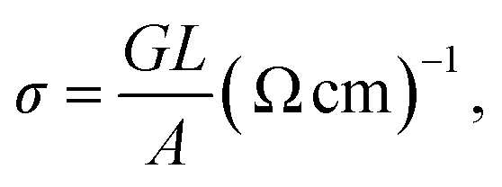
Transmission electron micrographs were taken using a Technai 20G2 (Philips) transmission electron microscope (TEM) equipped with a charge coupled device (CCD). The electrical properties of the thin films were measured with a Wayne Kerr precision impedance analyser (6500 P) in the frequency range of 20 Hz to 1 MHz. For these measurements, circular polymer films were cut and sandwiched between two circular silver discs and then placed between the two electrodes of the measuring cell. The contact area of the polymer films was 140.534 mm2, and the thickness was about 0.266 mm. The conductance G and the loss tangent D were measured with the help of the impedance values. The impedance analyser settings automatically controlled the temperature of the sample holder and monitored the data through the software. All measurements were carried out in the temperature range of 308–343 K, well below the glass transition temperature of the polymeric film.III. Results and discussion
A. Structural characterisation using transmission electron microscopy (TEM)
Cu-NPs prepared in different solvents were adhered onto a coated mesh, and the mesh was examined after being dried in a vacuum. Fig. 2A shows the microstructures of the copper NPs in SDS solution (a), acetone (b) and ethanol (c), and Fig. 2B shows the size distribution and particle size. The TEM images show that the copper NPs in different solvents have different shapes (shown in the respective insets). In the cases of SDS and acetone, the Cu NPs are hexagonal in shape with average particle sizes ranging from 12 to 25 nm and 15 to 30 nm, respectively. However, the Cu NPs prepared in ethanol are spherical with particle size varying between 20 and 40 nm. This results from medium effects; SDS may stabilise copper hydroxide and delay its conversion to copper oxide, whereas the nanoparticles may be complexed with the carbonyl group at their surfaces when prepared in acetone.22 In addition, the dipole moment of acetone is higher than that of ethanol, resulting in stronger bonds to the surface of NPs. This may also be due to the fact that the dielectric constant of acetone is less than that of ethanol. | ||
| Fig. 2 (A) The microstructures of copper NPs in SDS solution (a), acetone (b) and ethanol (c); insets show the individual nanoparticle shapes in different solvents. (B) Graphs of size distributions and particle sizes for NPs in different solvents. | ||
B. Electrical measurements
The frequency and temperature-dependent conductance G were measured using a impedance analyser. The conductivity was calculated by the following relation:
 | (1) |
 | ||
| Fig. 3 Variation in electrical conductivity versus frequency of polymeric films in the presence of Tb3+ ion and Tb3+ ion plus Cu NPs in different solvents in the temperature range of 308–343 K. | ||
The combined impedance of a sample is expressed as Z = Z′ − iZ′′, where Z′ and Z′′ are the real and imaginary parts of impedance, respectively. These values are calculated from the following relation:
 | (2) |
 | ||
| Fig. 4 Cole–Cole plots of polymeric films in the presence of Tb3+ ion and Tb3+ ion with Cu NPs in different solvents at a temperature of 323 K (50 °C). | ||
The bulk resistances Rb of the polymer films were calculated from the intercepts of the semicircle in Fig. 4 with the x-axis. The resistances of the polymer films at 323 K were found to be 2.7 × 10⁶ Ω, 1.8 × 10⁶ Ω, 4.5 × 10⁵ Ω and 5.6 × 10⁴ Ω for samples 1, 2, 3 and 4, respectively. Thus, the maximum resistance is found for the film with Tb3+ in PVA, and the minimum resistance corresponds to the film with Tb3+ and Cu NPs in ethanol. The bulk conductivities of the samples were calculated using the relation:
 | (3) |
The bulk conductivities σb for all four samples are plotted in Arrhenius form in Fig. 5(a). It is clear from the figure that the systems exhibit linear behaviour in the temperature region of 308–343 K. The activation energy for conduction was calculated using the Arrhenius relation:
 | (4) |
σbT [(ohm cm)−1 K] and 1000/T (K−1); the values thus obtained for the four samples are tabulated in Table 1. A decreasing trend in activation energy is clearly evident from sample 1 to sample 4. This corresponds to increasing electrical conductivity moving from the polymer film with Tb3+ alone to that with PVA, Tb3+ and Cu NPs in ethanol.
 | ||
| Fig. 5 (a) Arrhenius representation of bulk conductivity and (b) variation in the bulk conductivity of polymeric films in the presence of Tb3+ ion and Tb3+ ion plus Cu NPs in different solvents. | ||
| Sample | Activation energy |
|---|---|
| 308–343 K | |
| PVA + Tb ion (sample 1) | 0.26 eV |
| PVA + Tb ion + Cu NPs in SDS with water (sample 2) | 0.11 eV |
| PVA + Tb ion + Cu NPs in acetone (sample 3) | 0.10 eV |
| PVA + Tb ion + Cu NPs in ethanol (sample 4) | 0.02 eV |
The variation in the conductivity of the polymeric samples in different solvents at 323 K is shown in Fig. 5(b). The increase in conductivity from sample 1 to sample 4 can be understood as follows. In sample 1, when only Tb3+ ions are dispersed in PVA, the conduction is due to Tb3+ ions moving through the cross-linked PVA chains. In sample 2, which contains PVA with Tb3+ and Cu NPs in SDS solution, the conduction is due to Cu NPs moving through matrix consisting of PVA + Tb3+ cross-linked chains. Individual Cu NPs and Tb3+ ions migrate among the vacant sites of the cross-linked chains. The Cu-NPs increase in size and are agglomerated in acetone. Due to the larger particle sizes, small islands are formed in sample 3, which contains PVA with Tb3+ and laser-ablated Cu NPs in acetone. This provides more conducting channels for the system, enhancing the conductivity. In sample 4, which contains PVA with Tb3+ and Cu NPs in ethanol, the further improvement in particle size provides more conducting channels for the free ions. This causes a further increase in conductivity in sample 4. The observed conductivity phenomenon for all four samples explained above is diagrammed in Fig. 6. The TEM micrographs and corresponding particle size graphs (Fig. 2) also confirm the increase in particle size moving from sample 2 to sample 4. This confirms our hypothesis explaining the increases in conductivity.
 | ||
| Fig. 6 Pictorial representation of the conductivity phenomenon of Tb3+ ion in polymer films with copper NPs in different solvents. | ||
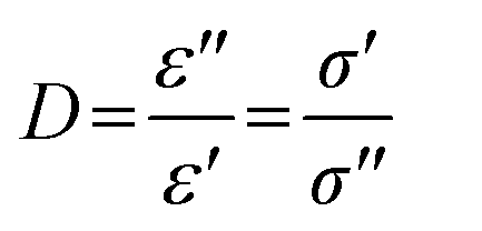
To further confirm the enhanced electrical conductivity, we show the variation in loss tangent with temperature at constant frequency in Fig. 7(a–c) for all four samples at 10 kHz (Fig. 7a), 100 kHz (Fig. 7b) and 1 MHz (Fig. 7c). These figures clearly show that the loss tangents are low for all samples, but they show an increasing trend moving from sample 1 to sample 4 (with the exceptions of the first two points of sample 4 and the last two points of sample 2 in Fig. 7a). For any frequency, the loss tangent is greatest for sample 4 (i.e., PVA with Tb3+ and Cu nanoparticles in ethanol). The loss tangent D is actually defined as:
 | (5) |
 | ||
| Fig. 7 Variation in loss tangent with temperature at constant frequency for the polymeric films. | ||
IV. Conclusions
Cu-NPs have been prepared in different solvents by laser ablation using a 1064 nm pulsed Nd-YAG laser. The TEM micrographs show hexagonally-shaped Cu NPs in the case of SDS solution and acetone and larger spherical NPs in the case of ethanol. The electrical properties of Tb3+ ions in PVA polymer films with Cu NPs in different solvents have been studied. It is concluded that the electrical conductivity of Tb3+ in polymer films is the greatest in the presence of larger spherical Cu NPs prepared in ethanol. It is proposed that the bigger size of the nanoparticles in ethanol forms more islands in the polymer matrix, enhancing the electrical conductivity of the film. The activation energy and variation in loss tangent with temperature also confirm the enhanced electrical behaviours of the samples.Acknowledgements
B. Kumar would like to acknowledge UGC for the Meritorious Fellowship in Science, and G. Kaur would like to acknowledge DST for a project grant.References
- M. C. Daniel and D. Astruc, Chem. Rev., 2004, 104, 293 CrossRef CAS PubMed.
- W. Zhang, X. Qiao and J. Chen, Mater. Sci. Eng., B, 2007, 142, 1 CrossRef CAS PubMed.
- F. Mafune, J. Y. Kohno, Y. Takeda and T. Kondow, J. Phys. Chem. B, 2003, 107, 4218 CrossRef CAS.
- S. Yang, W. Cai, H. Zhang, X. Xu and H. Zeng, J. Phys. Chem. C, 2009, 113, 19091 CAS.
- A. Santagata, A. D. Bonis, A. D. Giacomo, M. D. Aglio, A. Laurita, G. S. Senesi, R. Gaudiuso, S. Orlando, R. Teghil and G. P. Parisi, J. Phys. Chem. C, 2011, 115, 5160 CAS.
- S. Husam, A. Salman and M. J. Abdullah, Mater. Sci. Eng., B, 2013, 178, 1048 CrossRef PubMed.
- X. Ren, D. Chen and F. Tang, J. Phys. Chem. B, 2005, 109, 15803 CrossRef CAS PubMed.
- S. H. Wu and D. H. Chen, J. Colloid Interface Sci., 2004, 273, 165 CrossRef CAS PubMed.
- B. Kumar, G. Kaur, P. Singh and S. B. Rai, Appl. Phys. B, 2013, 110, 345 CrossRef CAS.
- P. V. Kazakevich, V. V. Voronov, A. V. Simakin and G. A. Shafeev, Quantum Electron., 2004, 34, 951 CrossRef CAS PubMed.
- H. L. Aye, S. Choopun and T. Chairuangsri, Adv. Mater. Res., 2010, 93, 83 CrossRef PubMed.
- V. Amendola and M. Meneghetti, Phys. Chem. Chem. Phys., 2009, 11, 3805 RSC.
- F. Bouchait, C. Champeaux, H. S. Nagaraja, F. Rossignol, N. Lory, A. Catherinot, P. Blondy and D. Cros, Thin Solid Films, 2004, 435, 269 Search PubMed.
- I. Dokme, S. Altındal, T. Tunc and I. Uslu, Microelectron. Reliab., 2010, 50, 39 CrossRef PubMed.
- D. D. Brunelli, T. D. Z. Atvars, I. Joekes and V. C. Barbosa, J. Appl. Polym. Sci., 1998, 69, 645 CrossRef.
- G. Kaur, R. K. Verma, D. K. Rai and S. B. Rai, J. Lumin., 2012, 132, 1683 CrossRef CAS PubMed.
- T. N. Rostovshchikov, V. V. Smirnov, V. M. Kozhevin, D. A. Yavsin, M. A. Zabelin, I. N. Yassievich and S. A. Gurevich, Appl. Catal., A, 2005, 296, 70 CrossRef PubMed.
- D. K. Sardar, K. L. Nash, R. M. Yow and J. B. Gruber, J. Appl. Phys., 2007, 101, 113115 CrossRef PubMed.
- E. Filippo, A. Serra and D. Manno, Sens. Actuators, B, 2009, 13, 625 CrossRef PubMed.
- M. Valodkar, P. S. Rathore, P. Sharma, D. Kanchan, M. Patel and S. Thakorea, Polym. Int., 2012, 61, 1745 CAS.
- A. Bose, S. Basu, S. Banerjee and D. Chakravorty, J. Appl. Phys., 2005, 98, 074307 CrossRef PubMed.
- B. Kumar, G. Kaur, and S. B. Rai, Indian J. Phys. DOI:10.1007/s12648-014-0617-0.
- K. Funke, C. Cramer and D. Wilmer, in Diffusion in Condensed Matter, ed. P. Heitjans and J. Kärger, Sringer, Berlin, 2004 Search PubMed.
- C. G. Raptis, A. Patsidis and G. C. Psarras, eXPRESS Polym. Lett., 2010, 4, 234 CrossRef CAS.
- U. Sasikala, P. N. Kumar, V. V. R. N. Rao and A. K. Sharma, Int. J. Adv. Sci. Eng. Tech., 2012, 2, 722 Search PubMed.
- A. Karthikeyan, P. Vinatier and A. Levasseur, Bull. Mater. Sci., 2000, 23, 179 CrossRef CAS.
- M. Hema, S. Selvasekerapandian, A. Sakunthala, D. Arunkumar and H. Nithya, Phys. B, 2008, 403, 2740 CrossRef CAS PubMed.
| This journal is © The Royal Society of Chemistry 2015 |