
One-pot synthesis of cubic ZnSe entangled nanowires and hexagonal Se nanorods†
Pin-Ru Chena,
Shih-Jung Hoa,
Yih-Hsing Lob and
Hsueh-Shih Chen*a
aDepartment of Materials Science and Engineering, National Tsing Hua University, Hsinchu 300, Taiwan. E-mail: chenhs@mx.nthu.edu.tw
bDepartment of Applied Physics and Chemistry, University of Taipei, Taipei 100, Taiwan
First published on 14th October 2014
Abstract
Se nanorods, ZnSe nanowires and their mixture can be prepared by a single process at different reaction temperatures between 300 to 360 °C. The Se nanorods are generally longer than 1 μm, while the ZnSe nanowires have an entangled structure and have a diameter and length of 15–20 nm and 0.3–2 μm, respectively.
Control over size and morphology of semiconductive nanomaterials to tailor their physical properties has been developed for decades.1 Nowadays, scientists are able to precisely control size/size distribution2 and shape/morphology of some II–VI and III–V semiconductive nanocrystals such as CdSe and InAs materials.3 ZnSe is one of the most famous wide bandgap semiconductive materials (Eg ∼ 2.7 eV) and its nanostructures have been extensively studied in the recent decade.4,5 Some synthetic methods have been reported for preparing ZnSe nanostructures, for example, wet-chemical methods5 and vacuum-based approaches.6 On the other hand, Se is also a well-known semiconductor with superior electrical and photoconductive properties. Recently, Se nanowires (NWs) have attracted much attention due to their phase- and size-dependent photoconductivity properties.7 The Se NWs showed improved photoconductance because of high surface-area-to-volume ratio and enhanced scattering of the incoming beam. So they have been considered a candidate in some optoelectronic applications such as phase-change memory, photodetection, solar cells and so on.8 At the moment, reports about synthesis of Se nanostructures are still few and most of reported synthetic approaches were based on the so-called two-stage method.9
In this communication, we report a wet-chemical process, in which hexagonal Se nanorods (NRs), cubic ZnSe entangling nanowires (E-NWs) or a mixture of the Se NRs/ZnSe E-NWs can be prepared at different reaction temperatures. In particular, the ZnSe nanowires synthesized possess entangling structure that would be first observed in ZnSe nanostructures. The synthetic process is similar to that of conventional ZnSe quantum dots (QDs) prepared from ZnO reported previously,4b–e except linear-chain carboxylic acids were replaced by an aromatic dicarboxylic acid, that is, isophthalic acid (IPA). IPA is an aromatic dicarboxylic acid with two highly polar dicarboxylic functional groups, which can act as ligands for metal ions. They have been used for preparation of metal–organic nanostructures in recent studies.10
The synthetic process and a precursor are slightly different from a previous method for ZnSe QDs.4b 3 mmol ZnO powder, 40 mmol isophthalic acid (benzene-1,3-dicarboxylic acid or meta-phthalic acid, C8H6O4, IPA, 99%) and 20 mmol trioctylphosphine oxide (C24H51PO, TOPO, 95%) first heated at 150 °C for 40 minutes under Ar flow, followed by dwelling at 350 °C for another 30 minutes. Trioctylphosphine selenide (TOPSe) was prepared by dissolving 3 mmol Se powder in 6 mmol trioctylphosphine (TOP, 90%). Injection temperatures of TOPSe were set to 300, 330 and 360 °C for Se NRs, mixture of Se NRs and ZnSe entangling nanowires (E-NWs), and ZnSe E-NWs, respectively. Growth temperatures were kept the same as the injection ones. In a typical synthesis, products were generated after reacting for 20 minutes. Samples were separated from the reaction liquid by a washing process. 50 ml methanol was poured into the reaction vessel at 120 °C, followed by mechanically mixing for 30 minutes under Ar flow. Then, the mixture was transferred into an ultrasonic bath at 50 °C for another 30 minutes, followed by centrifugation to remove remained organics for three times. Finally, samples were dried at room temperature in a vacuum chamber.
Fig. 1a shows XRD patterns of products when injection/growth temperatures of TOPSe are 300, 330 and 360 °C. The hexagonal Se and cubic zincblende ZnSe crystals are obtained when the reaction temperatures are 300 and 360 °C, respectively. A mixture of Se and ZnSe crystals is produced at 330 °C. From inductively coupled plasma-atomic emission spectrometer (ICP-AES) compositional analysis, the products obtained at 300, 330 and 360 °C contains Zn (3.8 mol%)/Se (96.2 mol%), Zn (19.1 mol%)/Se (80.9 mol%) and Zn (47.0 mol%)/Se (53.0 mol%), respectively. For the sample prepared at 330 °C, it contains yarn-ball-like entangling nanowires (E-NWs) and lager nanorods (NRs) according to scanning electron microscope (SEM) image (Fig. 1b), which is identified as ZnSe and Se, respectively by energy dispersive spectroscopy (EDS) on SEM (insets in Fig. 1b). Both of ZnSe and Se have some C, P and O signals, which can be ascribed to the remained organics used in the synthesis. A mixture of ZnSe E-NWs and Se NRs directly produced from a single reaction is interesting and promising as ZnSe and Se are native n-type and p-type semiconductors, respectively.
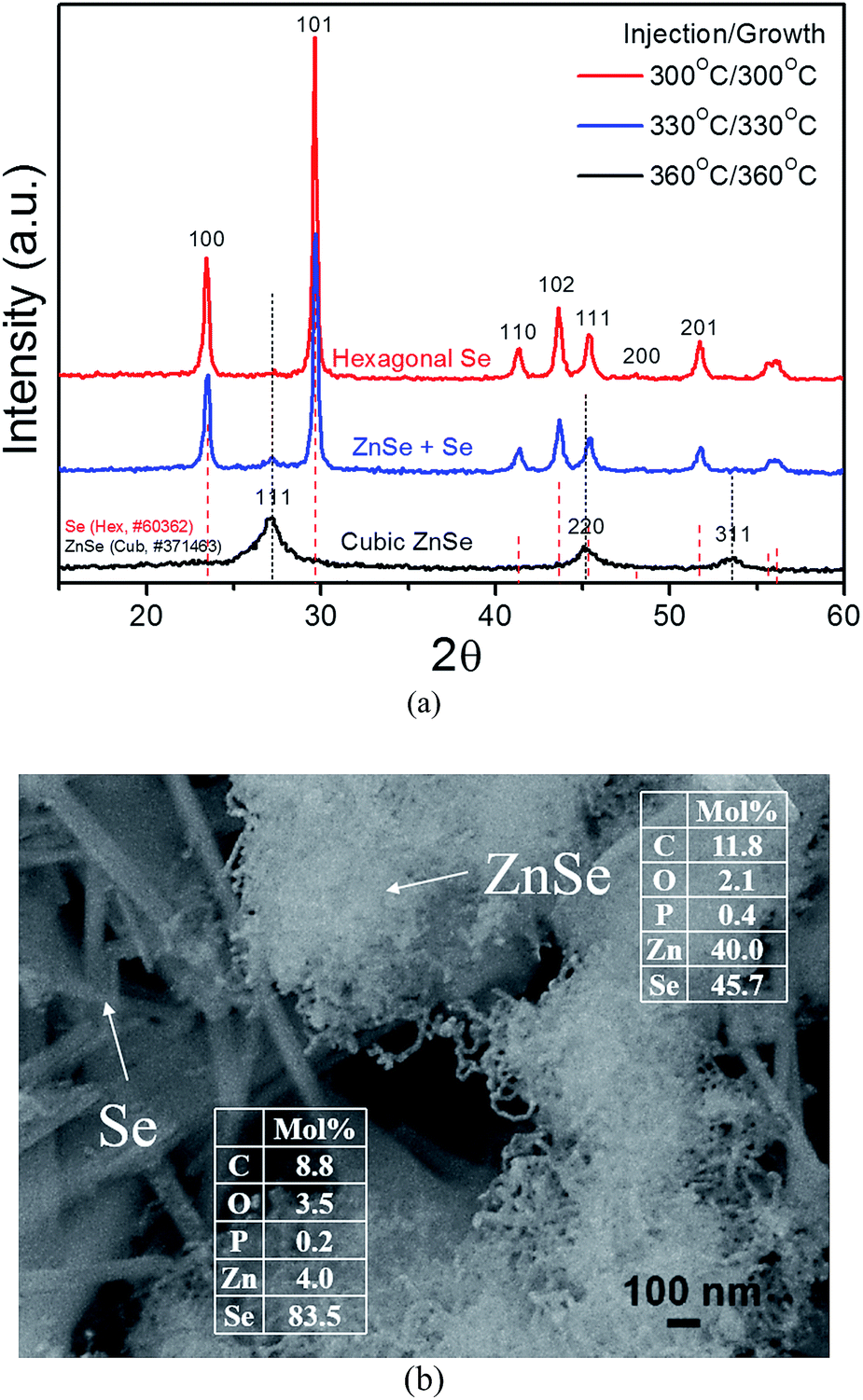 | ||
| Fig. 1 (a) XRD of products prepared from ZnO–IA–TOPO and TOPSe at 300, 330 and 360 °C. (b) SEM image and EDS data of samples synthesized at 330 °C. | ||
For a reaction at 360 °C, low-magnification SEM image (Fig. 2a) shows that micron-scaled yarn balls composed of ZnSe E-NWs are obtained. A high-resolution SEM image shows that the NWs are generally with the diameter of 15–20 nm and the stretched length of 300–2000 nm, as shown in Fig. 2b. A representative transmission electron microscope (TEM) image of the sample in Fig. 2c clearly shows that the ZnSe E-NWs are nanowires with some folding structures, which are rarely seen for crystals since the crystal growth is either isotropic or anisotropic and thus they normally form a particulate structure or a crystal with a preferred orientation. Fig. 2d shows a high resolution TEM image of a ZnSe NW. The dashed lined region M appears to be a short rod connected with two other rods at the ends. The region N displays domain boundaries (regions X & Y in the right image) at the joint of the ZnSe NW, suggesting that two individual crystals are merged into a crystal. The Moiré pattern (red arrows) at the joint part further supports that two mis-orientated crystals overlap each other (higher resolution image is in ESI†). Top-right inset in Fig. 2d schematically shows a Moiré pattern generated from two overlapped line sets with equal space. Based on the above results, it is suggested that the growth of the folding ZnSe NWs is based on the oriented growth mechanism.11 Indeed, unlike II–VI materials with hexagonal wurtzite structure that is intrinsically anisotropic and feasibly grow along the c-axis, the growth of cubic zincblende ZnSe would tend to be in a cubic morphology. Consequently, it is reasonable to propose that the oriented attachment is one of the growth modes for anisotropic growth for crystals with the cubic structure. This may explain that the ZnSe crystal does not consistently grow in a single orientation since individual crystals may attach to the crystal facets similar to them, e.g., four {111} facets or different facets with the similar lattice constant. The detailed growth mechanism needs further investigation, however, it is believed that the oriented growth is caused by IPA because spherical or polyhedral ZnSe nanocrystals could be produced when IPA was simply replaced by stearic acid or lauric acid respectively, which have been shown in our previous studies.4b,e,f Photoluminescence spectrum from ZnSe E-NWs is shown in Fig. 3. The E-NWs emit near-UV light (λem ∼ 398 nm) under excitation of 325 nm He–Cd laser (∼40 mW), which is promising in optoelectronic applications. A small peak between 750–800 nm is assigned to the surface or interface state emission, implying that some defects exist in the ZnSe E-NWs, which might be related to the surface traps and/or defects in the rod boundary.
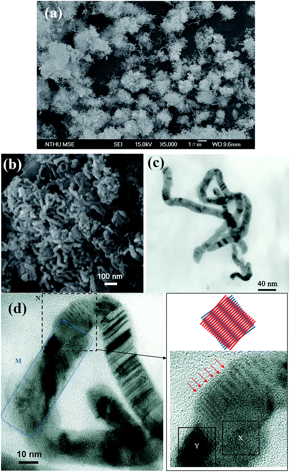 | ||
| Fig. 2 (a) Entangled ZnSe nanowires display a yarn-ball-like morphology in a low-magnification SEM image. (b) A selected ZnSe yarn ball composed of E-NWs in a high-magnification SEM image. (c) ZnSe NWs entangle themselves and form a knot-like structure in a TEM image. (d) High-resolution TEM image shows a joint of the NWs in (c). Region M appears to be a short rod. Dashed square N exhibits a Moiré pattern (arrows on the right image). Inset at the right schematically shows a Moiré pattern from two line sets (with equal space) misoriented. The folding structure can keep some space among the rods and avoid aggregation. | ||
 | ||
| Fig. 3 Photoluminescence spectrum from ZnSe E-NWs (λex = 325 nm, He–Cd laser, 40 mW). | ||
In general, straight NWs easily become agglomerate. For the yarn-ball-like ZnSe E-NWs, their entangling structure may be useful because the folding structure is a kind of 3D structure that keeps some space among NWs and allows polymer chains to easily intercalate into the NW network, as shown in Fig. 2d. So it may be beneficial to improve the phase stability or thermal stability of organic–inorganic hybrid. Fig. 4 shows the thermogravimetric analysis (TGA) results of Kapton polyimide (PI), PI/ZnSe nanoparticles (concentration = 3 phr, d ∼ 7.5 nm) and PI/ZnSe E-NWs hybrids (concentration = 3 phr). Temperatures of 10% thermal decomposition of PI, PI/NPs and PI/E-NWs are 563, 577 and 614 °C, respectively, showing that the entangling structure significantly improves the thermal stability of conventional polyimide and is ascribed to a higher degree of hybridization.12 A slight weight loss of PI/ZnSe E-NWs is ascribed to the surfactants used in the synthesis. The inset image in Fig. 4 schematically shows the PI, PI incorporated NPs and PI interlaced with E-NWs. The mixed PI chains and entangling NWs delays the thermal decomposition of polymers.
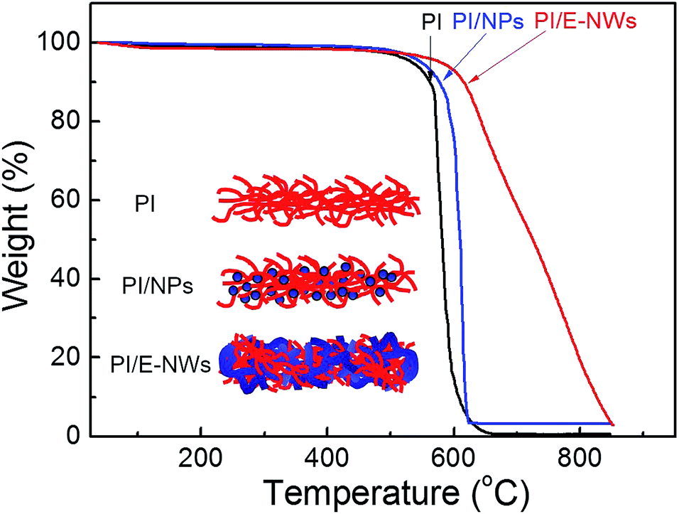 | ||
| Fig. 4 TGA data of PI, PI/NPs and PI/E-NWs. The inset image schematically shows mixtures of PI, PI/NPs and PI/E-NWs. | ||
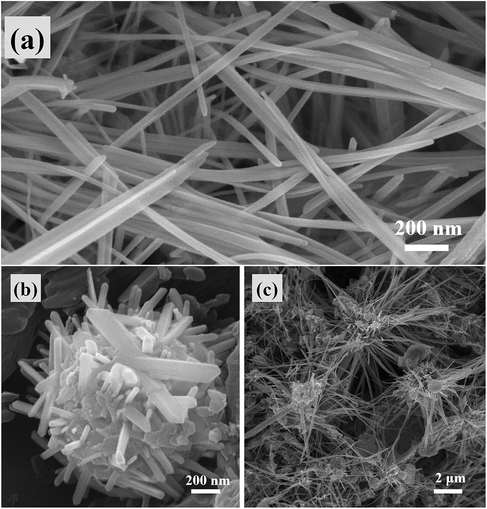
On the other hand, Se were obtained when reaction temperature was set at 300 °C. The product predominately contains Se NRs with the length generally longer than 1 μm, as shown in SEM images (Fig. 5a). The Se NRs appear to be long rectangle slabs, as shown in a higher resolution image in the inset. Some of the NRs are with morphology of semicircular tubes (ESI†). A TEM image of a short Se NR is shown in Fig. 5b. The Se NR was seemed to be structurally instable as it gradually turned into a tubular structure with lower crystallinity under exposure of electron beam, as shown in Fig. 5c. Another Se NR after an electron beam shower in a selected area shows a similar result, as shown in Fig. 5d.
 | ||
| Fig. 5 Se NRs synthesized by injecting TOPSe into ZnO–IA–TOPO mixture at 300 °C (growth time = 20 min). (a) SEM images of Se NRs dispersed on a piece of carbon tape. The inset shows a higher resolution image of Se NRs. Particles in the image are confirmed to be Se from EDS data (Se ∼ 94.5%). (b) TEM images of a selected Se NR. (c) The Se NR in image (b) after exposing to the electron beam for about 3 minutes (JEOL JEM 2010, operated at 200 keV). (d) Another Se NR exposed to the electron beam in a selected area. | ||
Previously, hexagonal trigonal Se NRs or NWs synthesized by wet-chemistry-based methods were reported.9 The growth of the hexagonal Se NRs was proposed to be via two stages, in which monodispersed amorphous Se (a-Se) spherical colloids first formed from reduction of selenious acid with excess hydrazine by refluxing at around 100 °C (first stage), followed by dissolution of the a-Se particles that supplied Se monomers to generate uniform hexagonal Se NWs after a couple of days (second stage).8b In contrast to the hexagonal Se NRs in the current study, the growth time was only a couple of hours, which is much faster than that of reported methods.
In order to examine the growth mechanism and the role of ZnO in the formation of Se NRs, we carried out a synthesis with the same process without ZnO as a reference. The result shows that similar Se NRs are obtained, as shown in a SEM image in Fig. 6a, which indicates that Zn-related complexes is not essential for the formation of Se NRs. However, the dimension (diameter and length) of Se NRs is slightly larger (∼20–40 nm) than those synthesized in the presence of ZnO, implying that ZnO might play a role in disturbing the crystal growth of Se NRs.
 | ||
| Fig. 6 (a) SEM images of Se NRs synthesized from thermal decomposition of TOPSe in a IA–TOPO mixture without ZnO. (b) Se NRs sampled at 10 min. (c) Se NRs sampled at 20 min. | ||
A SEM image of Se NRs sampled at 10 min after an injection of the Se precursor is in Fig. 6b. It shows that many short Se NRs exist on a micron-scaled particle, which is composed of 2 mol% P, 6 mol% O, 22% C, and 70 mol% Se according to an EDS analysis. Similar morphology is also observed in the product collected at 20 min (Fig. 6b). A lot of longer Se NRs appear to derive from the Se/organic particles. The urchin-like Se NRs suggest that the Se crystals grow from the Se/organic particles. It may propose that after TOPSe was injected into the IA–TOPO mixture, Se monomers were released to supply for nucleation and growth of NRs in the organic mixture.
In summary, we reported a synthetic approach to producing hexagonal Se nanorods, a mixture of hexagonal Se nanorods and cubic ZnSe entangling nanowires, and cubic ZnSe entangling nanowires from ZnO/isophthalic acid/trioctylphosphine oxide and trioctylphosphine selenide by controlling synthetic temperatures at 300, 330 and 360 °C, respectively. The Se nanorods were generally longer than 1 μm, while the ZnSe nanowires were with entangling structure and had the diameter and the length of 15–20 nm and 0.3–2 μm, respectively. Se NRs can be produced without ZnO, but the dimension of the NRs slightly increases.
Acknowledgements
This work was supported by the National Science Council of Taiwan under Contract no. NSC 102-2218-E-007-013-MY3. The authors acknowledge Miss Jhen-Yu Huang for XRD and TGA analyses.Notes and references
- (a) C. B. Murray, D. J. Norris and M. G. Bawendi, J. Am. Chem. Soc., 1993, 115, 8706 CrossRef CAS; (b) X. Peng, L. Manna, W. Yang, J. Wickham, E. Scher, A. Kadavanich and A. P. Alivisatos, Nature, 2000, 404, 59 CrossRef CAS PubMed; (c) A. B. Panda, S. Acharya and S. Efrima, Adv. Mater., 2005, 17, 2471 CrossRef CAS; (d) T. Ji, W. B. Jian and J. Fang, J. Am. Chem. Soc., 2003, 125, 8448 CrossRef CAS PubMed; (e) K. S. Cho, D. V. Talapin, W. Gaschler and C. B. Murray, J. Am. Chem. Soc., 2005, 127, 7140 CrossRef CAS PubMed.
- (a) H. S. Chen and R. V. Kumar, Cryst. Growth Des., 2009, 9, 4235 CrossRef CAS; (b) H. S. Chen and R. V. Kumar, J. Phys. Chem. C, 2009, 113, 31 CrossRef CAS; (c) H. S. Chen and R. V. Kumar, J. Phys. Chem. C, 2009, 113, 12236 CrossRef CAS; (d) H. S. Chen, H. Y. Hong and R. V. Kumar, J. Mater. Chem., 2011, 21, 5928 RSC; (e) H. S. Chen and R. V. Kumar, RSC Adv., 2012, 2, 11586 RSC; (f) H. S. Chen and R. V. Kumar, J. Nanopart. Res., 2012, 14, 1207 CrossRef.
- (a) X. Peng, L. Manna, W. Yang, J. Wickham, E. Scher, A. Kadavanich and A. P. Alivisatos, Nature, 2000, 404, 59 CrossRef CAS PubMed; (b) H. Yu and W. E. Buhro, Adv. Mater., 2003, 15, 416 CrossRef CAS; (c) S. M. Lee, S. N. Cho and J. Cheon, Adv. Mater., 2003, 15, 441 CrossRef CAS; (d) V. F. Puntes, K. M. Krishnan and A. P. Alivisatos, Science, 2001, 291, 2115 CrossRef CAS PubMed; (e) A. A. Guzelian, U. Banin, A. V. Kadavanich, X. Peng and A. P. Alivisatos, Appl. Phys. Lett., 1996, 69, 1432 CrossRef CAS PubMed.
- (a) D. J. Norris, N. Yao, F. T. Charnock and T. A. Kennedy, Nano Lett., 2001, 1, 3 CrossRef CAS; (b) H. S. Chen, B. Lo, J. Y. Hwang, G. Y. Chang, C. M. Chen, S. J. Tasi and S. J. Wang, J. Phys. Chem. B, 2004, 108, 17119 CrossRef CAS; (c) L. S. Li, N. Pradhan, Y. Wang and X. Peng, Nano Lett., 2004, 4, 2261 CrossRef CAS; (d) H. S. Chen, S. J. Wang, C. J. Lo and J. Y. Chi, Appl. Phys. Lett., 2005, 86, 131905 CrossRef PubMed; (e) H. S. Chen, H. Y. Horng and R. V. Kumar, Appl. Phys. Lett., 2009, 94, 141107 CrossRef PubMed; (f) H. S. Chen, B. Lo and J. Y. Huang, RSC Adv., 2014, 4, 2663 Search PubMed.
- (a) J. Xu, A. Lu, C. Wang, R. Zou, X. Liu, X. Wu, Y. Wang, S. Li, L. Sun, X. Chen, H. Oh, H. Baek, G. C. Yi and J. Chu, Adv. Eng. Mater., 2014, 16, 4459 CrossRef; (b) H. S. Song, W. J. Zhang, G. D. Yuan, Z. B. He, W. F. Zhang, Y. B. Tang, L. B. Luo, C. S. Lee, I. Bello and S. T. Lee, Appl. Phys. Lett., 2009, 95, 033117 CrossRef PubMed; (c) S. K. Chan, Y. Cai, N. Wang and I. K. Sou, Appl. Phys. Lett., 2006, 88, 013108 CrossRef PubMed; (d) U. Philipose, A. Saxena, H. E. Ruda, P. J. Simpson, Y. Q. Wang and K. L. Kavanagh, Nanotechnology, 2008, 19, 215715 CrossRef CAS PubMed; (e) Y. Zhang, Z. Wu, J. Zheng, X. Lin, H. Zhan, S. Li, J. Kang, J. Bleuse and H. Mariette, Sol. Energy Mater. Sol. Cells, 2012, 102, 15 CrossRef CAS PubMed; (f) B. Xiang, H. Z. Zhang, G. H. Li, F. H. Yang, F. H. Su, R. M. Wang, J. Xu, G. W. Lu, X. C. Sun, Q. Zhao and D. P. Yu, Appl. Phys. Lett., 2003, 82, 3330 CrossRef CAS PubMed; (g) P. T. K. Chin, J. W. Stouwdam and R. A. J. Janssen, Nano Lett., 2009, 9, 745 CrossRef CAS PubMed.
- (a) A. B. Panda, S. Acharya and S. Efrima, Adv. Mater., 2005, 17, 2471 CrossRef CAS; (b) D. Han, C. Song and X. Li, J. Nanomater., 2010, 290763 Search PubMed; (c) C. Yang, J. Wang, T. You and C. Zhang, Mater. Lett., 2012, 80, 29 CrossRef CAS PubMed.
- M. Yaman, T. Khudiyev, E. Ozgur, M. Kanik, O. Aktas, E. O. Ozgur, H. Deniz, E. Korkut and M. Bayindir, Nat. Mater., 2011, 10, 494 CrossRef CAS PubMed.
- (a) S. H. Lee, Y. Jung and R. Agarwal, Nat. Nanotechnol., 2007, 2, 626 CrossRef CAS PubMed; (b) W. Park, G. Zheng, X. Jiang, B. Tian and C. M. Lieber, Nano Lett., 2008, 8, 3004 CrossRef CAS PubMed; (c) L. Cao, P. Fan, A. P. Vasudev, J. S. White, Z. Yu, W. Cai, J. A. Schuller, S. Fan and M. L. Brongersma, Nano Lett., 2010, 10, 439 CrossRef CAS PubMed.
- (a) B. Gates, Y. Yin and Y. Xia, J. Am. Chem. Soc., 2000, 122, 12582 CrossRef CAS; (b) B. Gates, B. Mayers, B. Cattle and Y. Xia, Adv. Funct. Mater., 2002, 12, 219 CrossRef CAS; (c) U. Jeong, P. H. C. Camargo, Y. H. Lee and Y. Xia, J. Mater. Chem., 2006, 16, 3893 RSC; (d) J. M. Song, J. H. Zhu and S. H. Yu, J. Phys. Chem. B, 2006, 110, 23790 CrossRef CAS PubMed; (e) D. Yu, T. Jiang, F. Wang, Z. Wang, Y. Wang, W. Shi and X. Sun, CrystEngComm, 2009, 11, 1270 RSC.
- T. Panda, T. Kunduz and R. Banerjee, Chem. Commun., 2012, 48, 5464 RSC.
- (a) R. L. Penn and J. F. Banfield, Science, 1998, 281, 969 CrossRef CAS; (b) J. F. Banfield, S. A. Welch, H. Zhang, T. T. Ebert and R. L. Penn, Science, 2000, 289, 751 CrossRef CAS; (c) D. Li, M. H. Nielsen, J. R. I. Lee, C. Frandsen, J. F. Banfield and J. J. De Yoreo, Science, 2012, 336, 1014 CrossRef CAS PubMed.
- H. S. Chen, C. M. Chen and S. Y. Lee, Mater. Chem. Phys., 2006, 96, 244 CrossRef CAS PubMed.
Footnote |
| † Electronic supplementary information (ESI) available. See DOI: 10.1039/c4ra10308d |
| This journal is © The Royal Society of Chemistry 2014 |