TiO2@CdSe/CdS core–shell hollow nanospheres solar paint
Xiang Zhang,
Hongxia Sun,
Xiyun Tao and
Xingfu Zhou*
State Key Laboratory of Materials-Oriented Chemical Engineering, College of Chemistry and Chemical Engineering, Nanjing University of Technology, Nanjing, 210009, China. E-mail: zhouxf@njut.edu.cn
First published on 24th June 2014
Abstract
TiO2@CdSe/CdS core–shell hollow nanospheres solar paint was successfully prepared via hard template and ion exchange method considering the match of their band gap. The outer layer of TiO2 shell protects CdSe and CdS from decomposition and increases their stability. The diameters of the TiO2@CdSe/CdS hollow nanospheres were uniformly around 600 nm with a shell thickness of 70 nm. The visible light absorption onset of TiO2@CdSe/CdS hollow nanospheres is around 650 nm corresponding to a bandgap of 1.8 eV, showing a red-shift when compared with TiO2/CdS. TiO2@CdSe/CdS hollow nanospheres can be directly used as solar paint. The photoanode decorated by the solar paint performs a reliable photoelectric conversion efficiency of ∼0.79% and current density of 6.6 mA cm−2.
1. Introduction
There is a stringent global need for alternative, renewable energy sources for both economic and environmental reasons. One extremely attractive source of energy is the sun, which continuously transmits enormous quantities of light energy to earth. Can you imagine a kind of paint with a simple brush can convert light energy into electricity?The quantum dot-sensitized solar cell (QDSSC) has attracted tremendous research interests because of its excellent properties, such as photostability, high molar extinction coefficients, size-dependent optical properties, low costs and little environmental impact.1,2 It has also drawn significant attention as a feasible candidate for boosting the solar energy conversion efficiency owing to its theoretical maximum thermodynamic conversion efficiency as high as 44%.3 The employment of quantum dots (QD) as sensitizers in solar cells is mainly due to their tunable size-dependent properties, including multiple carrier generation (MEG), hot electron utilization and effective charge transfer.4,5 Due to the small size of quantum dots and the broad absorption area, QDSSC could capture nearly the entire incident solar light in the visible region.
The photoanode of QDSSC is typically a sensitized nanocrystalline TiO2 or ZnO film prepared by screen-print or doctor blade method, then sensitized by CdS, CdSe, PbS quantum dots. As is well known, sensitization is an important and essential process during the preparation of solar cell, which has a significant impact on the performance of the cell. Quantum dot sensitization is commonly performed by successive ion layer adsorption and reaction method (SILAR),4,6,7chemical bath deposition (CBD),8,9spray pyrolysis deposition (SPD),10–12 electrodeposition (ED)13,14 and so on. Irrespective of the kind of method, it is time-intensive, requiring multiple steps and a long time is needed to complete the integrity of photoanode film deposition and annealing protocols in order to attain the best performing cells. There are many kinds of quantum dots such as CdS,15,16 CdSe,17 InP,18 PbS,19,20 PbSe21 and InAs.22 Plenty of research has been carried out to improve the performance of quantum dot-sensitized solar cells. One such example utilizes a PbS and P25 heterojunction and is reported to exhibit a power conversion efficiency of 5.58% by Hg2+ doping into PbS.19 Quantum dot-sensitized solar cell research usually employs CdS and CdSe as co-sensitizers, whose relative band edges are 2.25 eV and 1.7 eV (ref. 20, 23 and 24) respectively, and a photoelectric conversion efficiency around 4–6 (ref. 5, 25–30) is usually achieved. However, the quantum dot used in QDSSC is usually unstable and leads to the decay of conversion efficiency in the air.
Considering quantum dot stability and the Fermi level alignment, we synthesized a kind of core–shell hollow sphere nanostructure. The configuration of the TiO2@CdSe/CdS hollow spheres (THS) is titanium dioxide in the outer shell layer, CdSe in the middle layer and CdS in the inner layer. Such a structure aims at injecting an excited electron from inner CdSe layer to outer TiO2 layer, transferring a hole out of inner CdSe to the electrolyte and then conducting it away. Further, we have prepared the energy level matching THS into the visible light responsive solar paint. As long as the obtained solar paint is simply brushed onto the surface of FTO, reliable photoelectric conversion efficiency of 0.79% with a current density of 6.6 mA cm−2 was achieved.
2. Results and discussion
The schematic diagram for the synthesis of TiO2@CdSe/CdS hollow spheres (THS) is shown in Fig. 1. The experiment was designed based on the case that the solubility product constant of CdS (∼7.94 × 10⁻²⁷) is much larger than that of CdSe (∼6.3 × 10−36). This implies that the CdS layer can be used as a sacrificial template for further transformation into more stable CdSe by anion exchange. First, templates SiO2 nanospheres were covered with CdS and TiO2 in order to form TiO2/CdS/SiO2 core–shell spheres. Then, the SiO2 cores were removed by hydrothermal treatment. Finally, the TiO2/CdS double-shelled hollow spheres (DHS) were infiltrated in the selenium source of the aqueous solution for several hours to obtain TiO2@CdSe/CdS hollow nanospheres. | ||
| Fig. 1 Schematic diagram of synthetic process of TiO2@CdSe/CdS hollow spheres. | ||
Fig. 2 shows the SEM images of the intermediate products obtained at each synthesis step. The digital inserting photograph shows an individual nanosphere obtained at synthesis step. Interestingly, the colour change is very obvious between each synthetic step, indicating the formation of different layer. From Fig. 2a to e, we can clearly see that the samples retain the spherical shape during synthesis. The average diameters of SiO2, CdS/SiO2, TiO2/CdS/SiO2, TiO2/CdS, TiO2@CdSe/CdS are around 500 nm, 550 nm, 590 nm, 590 nm, 590 nm, respectively, indicating that the thicknesses of CdS and TiO2 layer are both around 40 nm. As can be seen from the inset of Fig. 3d and e, the broken spheres demonstrate the existence of hollow structures. Hollow spherical THS are uniform with an average diameter of 590 nm. The thicknesses of the TiO2/CdS and TiO2@CdSe/CdS shells are around 90 nm, respectively, which correspond to the increase of the thickness during step 2 and step 3. It is also noted that the surface of the TiO2@CdSe/CdS hollow spheres is rougher than that of the TiO2/CdS. The rough CdSe shell is formed during their refluxed treatment in the selenium source of aqueous solution via ion exchange.
 | ||
| Fig. 2 SEM images of the products obtained in each synthesis steps. (a) SiO2. (b) CdS/SiO2. (c) TiO2/CdS/SiO2. (d) TiO2/CdS. (e) TiO2@CdSe/CdS, insets showing an individual nanosphere features. (f) XRD patterns for TiO2/CdS and TiO2@CdSe/CdS. | ||
 | ||
| Fig. 3 (a–c) TEM images of TiO2@CdSe/CdS hollow spheres, (d) HRTEM image of the circled area in (c). | ||
Fig. 2f shows the XRD patterns of TiO2/CdS (DHS) and TiO2@CdSe/CdS (THS) samples. Beside the diffraction peaks of anatase TiO2, diffraction peaks of hexagonal phase CdS and CdSe are also observed, indicating that three-shelled hollow spheres was successfully prepared. The broad diffraction peaks imply that the crystalline grains are on the nanoscale and well-crystallized. The average grain size is estimated according to the Scherrer equation by the full width at half maximum (FWHM) of the diffraction peaks. The average sizes of anatase TiO2, CdS and CdSe nanocrystals are about 13 nm, 10 nm and 5 nm respectively.
To further investigate the material of TiO2@CdSe/CdS hollow spheres, TEM has been performed to characterize the morphology. The TEM images of TiO2@CdSe/CdS are shown in Fig. 3. In Fig. 3a and b, the hollow spheres are uniformly in the same size, and the diameters of the hollow nanosphere can be estimated about 600 nm with a shell thickness of 70 nm. The color contrast between the fringe and central region in Fig. 3b confirms the existence of the hollow structure. Fig. 3c displays a broken hollow sphere, the inner surface could be observed. Fig. 3d showed the high resolution transmission electron microscopy (HRTEM) images. The distinct fringes in the HRTEM images provide the identification of the crystallographic spacing of TiO2, CdSe and CdS nanocrystals. The outboard lattice fringes of 0.35 nm correspond to the (101) crystal plane of anatase TiO2.12 The lattice fringes of 0.37 nm and 0.34 nm can be indexed to the (100) of CdSe and (002) of hexagonal CdS,1,30 respectively.
We measured the UV-visible absorption spectra of TiO2/CdS and TiO2@CdSe/CdS, which are shown in Fig. 4a. The absorption spectra can be easily ascribed to the variation of the energy band gaps (Eg) of those two semiconductor sensitizers. Eg for the TiO2/CdS and TiO2@CdSe/CdS can be estimated using the conventional Tauc equation by extrapolation of the linear part of the [F(R)hn]2 vs. hn plots31 (Fig. 4b). As we can see, the absorption spectra of the TiO2/CdS film shows absorption onset around 540 nm, which corresponds to a band gap of 2.2 eV. CdSe exhibits an enhanced light-harvesting effect, after the deposition of CdSe, the absorption edges were expanded observably. TiO2@CdSe/CdS shows a red-shift in the absorption with onset around 650 nm, which the band gap is 1.8 eV. As shown in the Fig. 4a, the black-brown colour of TiO2@CdSe/CdS films further ascertains the ability to capture the incident visible photons. The high absorbance in the visible region reveals the strong absorption properties of the TiO2@CdSe/CdS solar paint.
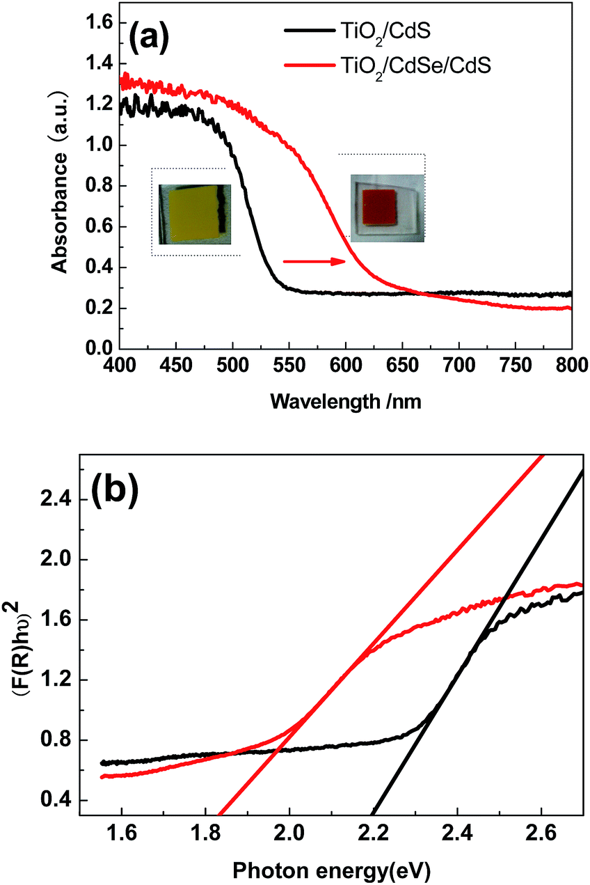 | ||
| Fig. 4 Optical properties of TiO2/CdS and TiO2@CdSe/CdSsolar paints, (a) the absorption spectra (b) display of the band gap extraction using Tauc Plot. | ||
We investigated the solar paint application under heat treatment in the air and N2 atmosphere. After calcination, the color is the same as the previously reported CdSe/CdS,32 indicating that the outer layer of TiO2 increased the thermal stability of CdSe and CdS. The J–V characteristics of these QDSCs are presented in Fig. 5. The detailed open circuit voltage (Voc), short circuit current (Jsc), fill factor (FF), and power conversion efficiency (Eff) are summarized in Table 1.
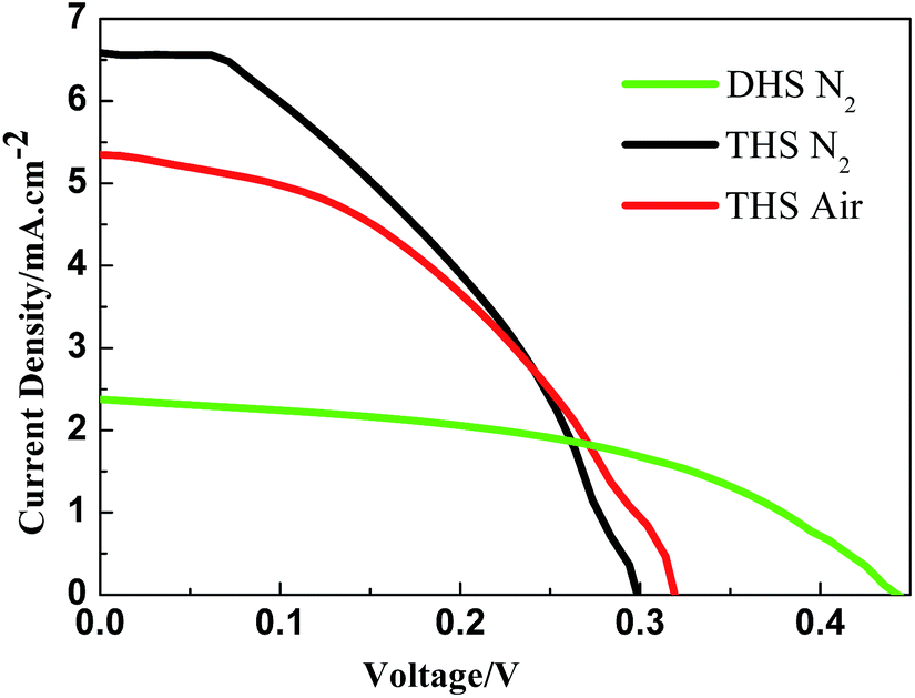 | ||
| Fig. 5 Photocurrent density–voltage (J–V) plot of TiO2/CdS and TiO2@CdSe/CdS solar paints under heat treatment in the air and N2 atmosphere. | ||
| Voc/V | Jsc/mA cm2 | FF (%) | Eff (%) | |
|---|---|---|---|---|
| DHS N2 | 0.47 | 2.38 | 48 | 0.54 |
| THS N2 | 0.30 | 6.58 | 42 | 0.79 |
| THS air | 0.32 | 5.46 | 44 | 0.74 |
The most striking feature observable in Fig. 5 is that the current density of THS is as much as twice higher than that of DHS. This may be attributed to CdSe and the novel hollow nanostructure of THS. The existence of CdSe, on one hand, increases the suction light range of THS. On the other hand, energy level matching of hollow structure can smoothen the conduction of electrons and holes, thereby increasing the electronic excitation and the cavity electronic separation. For THS, irrespective of whether the annealing treatment is carried out in air or in nitrogen atmosphere, there is not much difference. The voltage is higher in air, while a slightly higher current in nitrogen. This shows the stability of the TiO2@CdSe/CdS structure in air.
3. Conclusion
TiO2@CdSe/CdS hollow spheres were successfully fabricated via hard template and ion exchange route. The diameters of the TiO2@CdSe/CdS hollow nanospheres were uniformly around 600 nm with a shell thickness of 70 nm. The visible light absorption onset of TiO2@CdSe/CdS hollow nanospheres is around 650 nm corresponding to a bandgap of 1.8 eV, showing a red-shift when compared with TiO2/CdS. In addition, TiO2@CdSe/CdS hollow nanospheres can be directly used as solar paint. The photoanode decorated by the solar paint performs a reliable photoelectric conversion with an efficiency of ∼0.79% and a current density of 6.6 mA cm−2. The conversion efficiency changed slightly when TiO2@CdSe/CdS was annealed in N2 and air atmosphere. This is due to the outer layer of TiO2 protecting the inner CdSe and CdS from decomposition and increasing their stability. Further work is still in progress to convert sun light into electrical energy by using a facile solar paint.4. Experimental
1. General procedure for synthesis of TiO2@CdSe/CdS hollow spheres solar paint
Detailed synthesis procedure was depicted as follows:2. Preparation of solar paint and cell construction
TiO2@CdSe/CdSshell spheres were printed on a transparent conductive FTO (fluorine-doped tin oxide, 14 Ω per square, Nippon Sheet Glass, Japan) glass after dispersal in the ethanol solution containing ethyl cellulose and terpineol. This was followed by a sintering process at 450 °C for 30 minutes in air or in N2 atmosphere, respectively. The solar cells were assembled into a sandwich-type device by separating the counter electrode and the photoanode with a hot-melt gasket (25 μm, Surlyn1702, DuPont). The counter electrode used Cu2S, the construction of which is described elsewhere.19 A mixture of 1 M sodium sulfide and 1 M sulfur was employed as the electrolyte.3. Characterization
The morphology observations were examined by scanning electron microscope (SEM, FEI, Quanta-200) and field emission scanning electron microscopy (FESEM, Hitachi S-4800). The high-resolution transmission electron microscopy (HRTEM) investigation was carried out on a JEM-2010UHR instrument (JEOL, Japan), using an acceleration voltage of 200 kV. X-ray powder diffraction (XRD) data was collected by a Rigaku Smart Lab automatic diffractometer, with Cu-Kα radiation (λ = 1.541 Å) at 40 kV and 40 mA. The XRD patterns were recorded with a scanning increment of 0.05° at a scan speed of 0.02° second per step in the range of 10°–80° (2θ degree). The UV-vis diffuse reflectance spectra obtained of the as-prepared TiO2@CdSe/CdS films were measured by a UV-vis spectrophotometer (Persee, China). The I–V characteristics of the solar cells were measured using a Newport oriel solar simulator (model 94023A-450W) and Keithley 2420 source meter (USA) under simulated solar light (AM 1.5 G, 100 mW cm−2), which was calibrated with a standard silicon solar cell equipped with a filter. The active area of PSSC utilized in the I–V test was 0.16 cm2.Acknowledgements
This research was supported by the Natural Science Foundation of China (no. U1162108, no. 51272104); the Natural Science Foundation of Jiangsu Province Office of Education (no. 11KJA150002; no.10KJB150006), the Financial Foundation of State Key Laboratory of Materials-Oriented Chemical Engineering and A Project Funded by the Priority Academic Program Development of Jiangsu Higher Education Institutions.Notes and references
- R. S. Selinsky, Q. Ding, M. S. Faber, J. C. Wright and S. Jin, Chem. Soc. Rev., 2013, 42, 2963 RSC.
- Z. Yang, C. Y. Chen, P. Roy and H. T. Chang, Chem. Commun., 2011, 47, 9561 RSC.
- I. Morasero, S. Gimenez, F. S. Francisco, Q. Shen and J. Bisquert, Acc. Chem. Res., 2009, 42, 1848 CrossRef CAS PubMed.
- M. Shalom, Z. Tachan, Y. Bouhadana, H. N. Barad and A. Zaban, J. Phys. Chem. Lett., 2011, 2, 1998 CrossRef CAS.
- A. J. Nozik, Phys. E, 2002, 14, 115 CrossRef CAS.
- J. T. Margraf, A. Ruland, V. sgobba, D. M. Guldi and T. Clark, Langmuir, 2013, 29, 2434 CrossRef CAS PubMed.
- M. Shalom, S. Buhbut, S. Tirosh and A. Zaban, J. Phys. Chem. Lett., 2012, 3, 2436 CrossRef CAS.
- J. Yang, L. K. Pan, G. Zhu, X. J. Liu, H. C. Sun and Z. Sun, J. Electroanal. Chem., 2012, 677, 101 CrossRef PubMed.
- J. Li, L. Zhao, S. M. Zhao, J. H. Hu, B. H. Dong and H. B. Hu, Mater. Res. Bull., 2013, 48, 2566 CrossRef CAS PubMed.
- S. Kim, S. H. Im, M. Kang, J. H. Heo, S. I. Seok, S. W. Kim and I. Mora, Phys. Chem. Chem. Phys., 2012, 14, 14999 RSC.
- K. Shin, J. B. Yoo and J. H. Park, J. Power Sources, 2013, 225, 263 CrossRef CAS PubMed.
- G. Zhu, L. K. Pan, T. Xu and Z. Sun, ACS Appl. Mater. Interfaces, 2011, 3, 3146 CAS.
- L. C. Chen, Y. C. Ho, R. Y. Yang, J. H. Chen and C. M. Huang, Appl. Surf. Sci., 2012, 258, 6558 CrossRef CAS PubMed.
- J. Li, C. J. Lin, J. T. Li and Z. Q. Lin, Thin Solid Films, 2011, 519, 5494 CrossRef CAS PubMed.
- C. H. Chang and Y. L. Lee, Appl. Phys. Lett., 2007, 91, 535 Search PubMed.
- Y. L. Lee and C. H. Chang, J. Power Sources, 2008, 185, 584 CrossRef CAS PubMed.
- N. Biswal and K. M. Parida, Int. J. Hydrogen Energy, 2013, 38, 1267 CrossRef CAS PubMed.
- H. M. Chen, C. K. Chen, C. C. Lin, R. S. Liu, H. Yang, W. S. Chang, K. H. Chen, T. S. Chan, J. F. Lee and D. P. Tsai, J. Phys. Chem. C, 2011, 115, 21971 CAS.
- J. W. Lee, D. Y. Son, T. K. Ahn, H. W. Shin, I. Y. Kim, S. J. Hwang and N. G. Park, Sci. Rep., 2013, 3, 1050 Search PubMed.
- Y. L. Lee and Y. S. Lo, Adv. Funct. Mater., 2009, 19, 604 CrossRef.
- Z. H. Chen, S. Y. Yeung, H. Li, J. C. Qian, W. J. Zhang, Y. Y. Li and I. Bello, Nanoscale, 2012, 4, 3154 RSC.
- P. Yu, K. Zhu, A. G. Norman, S. Ferrere, A. J. Frank and A. J. Nozik, J. Phys. Chem. B, 2006, 110 Search PubMed.
- Z. X. Li, Y. L. Xie, H. Xu, T. M. Wang, G. Xu and H. L. Zhang, J. Photochem. Photobiol., A, 2011, 224, 25 CrossRef CAS PubMed.
- J. Yan, Q. Ye and F. Zhou, Adv. Mater., 2012, 2, 3978 CAS.
- E. H. Kong, Y. J. Chang, Y. C. Park, Y. H. Yoon, H. J. Park and H. M. Jang, Phys. Chem. Chem. Phys., 2012, 14, 4620 RSC.
- Y. K. Lai, Z. Q. Lin, D. J. Zheng, L. F. Chi, R. G. Du and C. J. Lin, Electrochim. Acta, 2012, 79, 175 CrossRef CAS PubMed.
- C. H. Li, L. Yang, J. Y. Xiao, Y. C. Wu and M. Sondergaard, Phys. Chem. Chem. Phys., 2013, 15, 8710 RSC.
- T. Toyoda, k. Oshikane, D. M. Li, Y. H. Luo, Q. B. Meng and Q. Shen, J. Appl. Phys., 2010, 108, 114304 CrossRef PubMed.
- Z. Zhu, J. H. Qiu, K. Y. Yan and S. H. Yang, ACS Appl. Mater. Interfaces, 2013, 5, 4000 CAS.
- P. K. Santra and P. V. Kamat, J. Am. Chem. Soc., 2012, 134, 2508 CrossRef CAS PubMed.
- J. J. Tian, Q. F. Zhang, L. L. Zhang and R. Gao, Nanoscale, 2013, 5, 936 RSC.
- Z. X. Pan, H. Zhou, K. Cheng, Y. Hou, J. Hua and X. Zhong, ACS Nano, 2012, 3982 CrossRef CAS PubMed.
| This journal is © The Royal Society of Chemistry 2014 |