DOI:
10.1039/D5RA01868D
(Paper)
RSC Adv., 2025,
15, 15618-15629
Direct correlation between open-circuit voltage and quasi-fermi level splitting in perovskite solar cells: a computational step involving thickness, doping, lifetime, and temperature variations for green solutions
Received
15th March 2025
, Accepted 27th April 2025
First published on 12th May 2025
Abstract
In this study, a 1D perovskite-based solar cell was simulated using COMSOL, incorporating CH3NH3GeI3 (organic in-organic hybrid) as an absorber layer, SnO2 as the electron transport layer (ETL), and Cu2Te as the hole transport layer (HTL). The simulations reveal that reducing the ETL's thickness enhances current density (J), although the maximum output power (Pmax) diminishes with ETL's thickness. Conversely, increasing the absorber layer's thickness boosts open-circuit voltage (Voc) and efficiency, exhibiting direct relation between Voc and quasi-Fermi level splitting. Furthermore, variations in HTL thickness do not significantly affect Voc or Pmax. Notably, Voc and Pmax both increase with acceptor density, conversely, increase in donor density leads to declines in both Voc and Pmax. While extending the electron–hole (e–h) lifetime within the ETL results in marginal efficiency improvements, significant enhancements in the e–h lifetime within the absorber layer substantially improve performance. However, the efficiency remains unaffected by variations in the e–h lifetime of the HTL. Additionally, higher operating temperatures adversely impact device performance, reducing J, Voc, Pmax, fill factor, and overall efficiency. This study provides critical insights into optimizing material properties and device parameters for experimental applications, underscoring the potential of CH3NH3GeI3-based perovskites as viable candidates for next-generation photovoltaic technologies.
1. Introduction
Global energy consumption has surged by over 50% in the past two decades, driving a corresponding rise in carbon dioxide emissions.1 The energy sector fulfils more than 80% of global energy demand and contributes approximately 75% of greenhouse gas emissions worldwide.2–4 With energy demand projected to grow by 25% in the coming years, renewable energy is expected to meet nearly 40% of the global supply by 2040, underscoring the critical need for sustainable solutions like solar energy.5 Among renewable sources, solar energy has gained significant traction due to its abundance and capacity to meet a substantial portion of global energy needs. In particular, perovskite solar cells (PSCs) have garnered attention for their high efficiency, low production costs, and ease of fabrication, with reported power conversion efficiencies (PCEs) reaching ∼25.5%.6,7 Approaching the performance of conventional silicon-based solar cells, PSCs represent a promising avenue for the global energy transition. The layered structure of PSCs comprises an electron transport layer (ETL), a perovskite absorber layer (PVK), and a hole transport layer (HTL), working synergistically to optimize light absorption and charge separation, critical for their efficiency and stability.8,9
The ETL plays a pivotal role in selectively transporting electrons from the PVK layer to the electrode while blocking holes, thereby minimizing recombination losses. Tin dioxide (SnO2) is a widely used ETL material due to its high electron mobility, wide bandgap (∼3.6 eV), and excellent optical transparency, enabling efficient electron conduction and sunlight penetration.10–13 Additionally, SnO2 offers superior thermal and chemical stability, can be fabricated at low temperatures, and resists degradation under UV exposure.14–17 Its compatibility with diverse fabrication methods, including sputtering and solution processing, further enhances its versatility. Collectively, these properties significantly boost the stability and efficiency of PSCs.
The PVK layer is the core of the solar cell, responsible for absorbing sunlight and generating electron–hole (e–h) pairs. For organic in-organic hybrid, lead (Pb)-free methylammonium germanium iodide (CH3NH3GeI3) serves as a greener alternative to conventional perovskites, achieving PCE exceeding 18.01%.18 Here, CH3NH3 is organic while Ge and I3 are in-organic parts in PVK material. Its high absorption and optimal bandgap (∼1.6 eV) facilitate efficient photon conversion across the visible spectrum.19,20 Furthermore, CH3NH3GeI3 offers long carrier diffusion lengths and high charge mobility, essential for reducing recombination losses and enhancing device performance.21 It exhibits a favorable tolerance factor (t = 0.97), which lies within the empirical range of 0.97–1.03, making it an ideal perovskite candidate.22 Although slightly distorted, this value is still considered within the acceptable margin for stable perovskite structures. Existing literature confirms the viability of MAGeI3 in photovoltaic application, highlighting its distorted orthorhombic or tetragonal symmetry—structurally comparable to MASnI3. In this context, various studies have explored the stability and electronic properties of Ge-based perovskites, identifying MAGeI3 as a promising, lead-free alternative.23–25
After optimizing the lattice parameters via VESTA, the cubic perovskite unit cell of CH3NH3GeI3's crystal structure is generated, as shown in Fig. 1(a). This material strikes an ideal balance between sustainability and photovoltaic (PV) efficiency, making it a strong candidate for next-generation solar cells.
 |
| | Fig. 1 (a) Crystal structure of CH3NH3GeI3 perovskite material, (b) energy band alignment of ETL, PVK layer, and HTL to ensure the smooth pathway for removal of electron and hole from absorbing layer towards respective electrodes, and (c) schematic illustration of working of solar cell highlighting the role of thicknesses of ETL, PVK, and HTL. | |
The HTL completes the charge separation process by extracting and transferring holes from the PVK layer to the electrode. Copper telluride (Cu2Te) is a promising HTL material, offering high hole conductivity (>100 cm2 V−1 s−1), excellent thermal and chemical stability, and proper energy level alignment with the PVK layer.26 Its high work function and p-type conductivity enhance hole extraction while minimizing recombination losses. Cu2Te also boasts a simple binary composition, low toxicity, earth abundance, a direct bandgap of ∼1.10 eV, and a notable absorption coefficient (>104 cm−1).27–30 These properties, coupled with its operational stability and scalability, make it a valuable component for improving the efficiency and longevity of PSCs.
In this study, we simulated 1D SnO2/CH3NH3GeI3/Cu2Te solar cell configuration observing the point ideal ohmic front and back contacts at room temperature. The SnO2/CH3NH3GeI3/Cu2Te configuration enhances PSC performance by maximizing charge transfer and reducing recombination losses. The precise energy band alignment among SnO2, CH3NH3GeI3 (MAGeI3), and Cu2Te, as shown in Fig. 1(b), is critical for optimizing charge dynamics and device performance. It can be seen that the energies of valence band (Ev), conduction band (Ec), electron fermi energy level (Efn), and hole fermi energy level (Efp) of each layer are well matching and ensuring the smooth pathway for the removal of electron and hole towards respective electrodes. SnO2's wide bandgap prevents electron recombination and directs electrons toward the top contact, while the alignment between MAGeI3 and Cu2Te facilitates efficient hole transport. This well-engineered SnO2/CH3NH3GeI3/Cu2Te architecture achieves efficient photon absorption, charge separation, and carrier transport with minimal recombination losses, demonstrating the potential for high-performance solar energy conversion at room temperature. This design not only boosts device efficiency and stability but also addresses environmental concerns through the use of non-toxic materials, positioning it as a viable solution for sustainable and efficient solar energy generation.
2. Numerical modelling
The primary objective of a solar cell is to understand how light-generated charge carriers (electrons and holes) respond to internal electric fields.31 The simulation process requires for solving three equations: the Poisson equation, the continuity equations for electrons and holes, and the current density (J) equations. Each equation plays a distinct role in characterizing the solar cell's overall behaviour. The Poisson equation (eqn (1) & (2)) governs the electrostatic potential generated by charge distribution within the device:| |
 | (1) |
| |
 | (2) |
Here in eqn (1) & (2), E represents electric field, Ψ denotes the electrostatic potential, q is the electron charge, and ε is the dielectric constant of the semiconductor material. The hole and electron concentrations are represented by p and n, respectively, while NA− and ND+ refer to the densities of ionized acceptors and donors, respectively. Additionally, ρt and nt represent the concentrations of trapped holes and electrons, respectively, and x is the position coordinate within the material.32 This formula connects the p–n junction parameter space charge with the electric field. The conservation of charge carriers in the device is described by the continuity equations (eqn (3) & (4)) for electrons and holes, which take into consideration the temporal and spatial fluctuations in carrier concentrations brought on by generation, recombination, diffusion, and drift in the electric field:| |
 | (3) |
| |
 | (4) |
Here, in eqn (3) & (4), for electrons, the generation and recombination rates are denoted by G and R, whereas the J is represented by Jn, while the comparable parameters for holes are represented as G, R, and Jp. These equations capture the charge carrier's movement and interaction under internal and external stimuli.33,34 In eqn (5) & (6), J describes the combined effects of drift and diffusion on charge carrier flow:| |
 | (5) |
| |
 | (6) |
Here, in eqn (5) & (6), q is the elementary charge, μn and μp are electron and hole mobilities, Dn and Dp are diffusion coefficients, and E is the electric field.35,36 The equations highlight the interplay between the electric field and concentration gradients. The generation rate of carries due to light absorption is given by (eqn (7)):Here, in eqn (7), I0 is the incident light intensity (AM 1.5 standard spectrum is taken as reference here), α is the absorption coefficient, and x represents depth.37 The exponential term describes the attenuation of light intensity as it penetrates the material. After generation of charge carriers, depending upon lifetime of these charge carrier, there happens recombination of charge carriers too. One of the types of recombination, there is Shockley–Read–Hall (SRH) recombination (and observed in this study), and it is given as (eqn (8)):| |
 | (8) |
This mechanism involves trap states or defects, with τn and τp denoting the lifetimes of electrons and holes.38 There may be the probability of radiative recombination in working of solar cell, so it is given as (eqn (9)):
Photons are produced by the recombination of electrons and holes in direct-bandgap semiconductors. Recombination is dependent on the product of electron and hole concentrations (np) and their equilibrium values n0p0, and the radiative recombination coefficient is denoted by B.39 These equations are discretized and solved over the geometry of the solar cell in COMSOL.40 By solving these equations concurrently, COMSOL offers a comprehensive simulation of the solar cell's performance, including efficiency, current–voltage characteristics, and other crucial parameters. The optimized initial parameters for 1D SnO2/CH3NH3GeI3/Cu2Te solar cell are tabulated in Table 1.
Table 1 The initial optimized parameters for 1D SnO2 (ETL)/CH3NH3GeI3 (PVK layer)/Cu2Te (HTL) solar cell
| Parameters |
ETL |
PVK |
HTL |
| Relative permittivity |
10 |
10 |
10 |
| Band gap (eV) |
3.5 |
1.9 |
1.19 |
| Electron affinity (eV) |
4 |
3.98 |
4.1 |
| Effective density of states, valence band (cm−3) |
2.2 × 10¹⁹ |
1 × 10¹⁶ |
1.8 × 10¹⁹ |
| Effective density of states, conduction band (cm−3) |
2.2 × 10¹⁸ |
1 × 10¹⁵ |
7.8 × 10¹⁷ |
| Electron mobility (m2 V−1 s−1) |
50 |
16.2 |
500 |
| Hole mobility (m2 V−1 s−1) |
12 |
2.1 |
100 |
| Electron lifetime, SRH (ns) |
1000 |
1 |
1 |
| Hole lifetime, SRH (ns) |
1000 |
1 |
1 |
3. Results and discussion
3.1 Effect of ETL thickness on solar cell performance
The ETL, PVK layer, and HTL are considered as pivotal layers in solar cell formation, and their thicknesses play a critical role in the output performance, as illustrated schematically in Fig. 1(c). The thinner ETL exhibits higher current densities due to efficient charge transport, as electrons generated in the absorber layer encounter minimal resistance while traversing the ETL. So, to analyze the effect of different ETL thicknesses on solar cell performance, it is varied from 10–90 nm, and current density–voltage (J–V) and power–voltage (P–V) characteristics are shown in Fig. 2(a). The P–V characteristics, indicating that maximum power output (Pmax) decreases with increasing ETL thickness due to resistive losses and recombination effects, which reduce optical transmittance and become more pronounced at higher voltages.41,42 Fig. 2(b) present the variation in short-circuit current density (Jsc), open-circuit voltage (Voc), Pmax, fill factor (FF), and efficiency, showing that thinner ETLs (∼10 nm) yield higher Jsc (179.940 A m−2) due to reduced resistance and improved charge collection efficiency, enabling more photogenerated electrons to reach the contacts. The Voc remains relatively constant (1.011 V at 10 nm and 1.009 at 90 nm) across a range of ETL thicknesses, as Voc is primarily determined by material properties and energy level alignment at interfaces, with SnO2 maintaining effective energy alignment irrespective of thickness. The Pmax shows a significant decline (from 155.043–129.420 W) as ETL thickness increases (from 10–90 nm), driven by higher series resistance (Rs) and recombination losses associated with thicker ETLs, which impairs overall device performance. Similarly, the FF slightly declines (from 85.226–84.989%) with increasing ETL thickness due to rising Rs, which hampers efficient electron transport and reduces the device's ability to transmit power under ideal conditions. Finally, the power-dependent efficiency declines largely from 15.504% at 10 nm to 12.942% at 90 nm. Table 2 presents the detailed values of output characteristics of 1D SnO2/CH3NH3GeI3/Cu2Te solar cell at different ETL's thicknesses.
 |
| | Fig. 2 (a) J–V and P–V characteristics at different ETL thicknesses (nm), and its effect on (b) Jsc, Voc, Pmax, FF, and efficiency, (c) J–V and P–V curves at different PVK thicknesses (nm), and its effect on (d) Jsc, Voc, Pmax, FF, and efficiency, (e) J–V and P–V response at different HTL thicknesses (nm), and its effect on (f) Jsc, Voc, Pmax, FF, and efficiency. | |
Table 2 The effect of ETL's thicknesses on output characteristics of 1D SnO2/CH3NH3GeI3/Cu2Te solar cell
| ETL thickness (nm) |
Jsc (A m−2) |
Voc (V) |
Pmax (W) |
FF (%) |
Efficiency (%) |
| 10 |
179.940 |
1.011 |
155.043 |
85.226 |
15.504 |
| 30 |
170.410 |
1.010 |
146.475 |
85.103 |
14.647 |
| 50 |
162.490 |
1.010 |
139.653 |
85.094 |
13.965 |
| 70 |
156.190 |
1.009 |
134.064 |
85.068 |
13.406 |
| 90 |
150.920 |
1.009 |
129.420 |
84.989 |
12.942 |
3.2 Effect of PVK thickness on solar cell performance
The J–V characteristics reveal that thicker absorber layers enhance photon absorption, generating more e–h pairs and increasing J, as shown in Fig. 2(c).43–46 However, beyond an optimal thickness (around 700 nm), resistive and recombination losses escalate, impairing charge collection efficiency and causing a decline in J, particularly at higher voltages. Similarly, the P–V characteristics show that thicker layers improve absorption and charge generation, excessive thickness introduces resistive and recombination losses, reducing power output and illustrating the trade-off between absorption and recombination, as shown in Fig. 2(c). Fig. 2(d) shows that the Jsc increases (from 69.30–167.22 A m−2) with absorber thickness (ranging from 100–900 nm), due to enhanced light absorption and charge carrier generation. However, as thickness increases, light absorption saturates, and additional thickness amplifies recombination rates, limiting effective charge collection, and consequently exhibits asymptotic behaviour beyond a certain thickness. In contrast, the Voc initially rises with thickness (1.10 V at 100 nm and 1.20 V at 900 nm) due to improved light absorption and quasi-Fermi level splitting, exhibiting direct relation between Voc and quasi-Fermi level splitting, as shown in Fig. 2(d). Nevertheless, Voc saturates (∼1.203 V) beyond a threshold thickness as resistive and recombination losses counterbalance further carrier generation gains. Moreover, Fig. 2(d) expresses that the Pmax increases from 68.06 at 100 nm to 120.69 W at 700 nm but then starts to decline (117 W at 900 nm) due to elevated resistive and recombination losses. Furthermore, the FF diminishes as thickness increase (from 88.52% at 100 nm to 58% at 900 nm), as shown in Fig. 2(d), because higher resistive and recombination losses hinder the device's ability to operate near its optimal power point. Finally, the efficiency initially improves with absorber thickness (from 6.8 to 12.06% within 100 to 700 nm) due to enhanced light absorption and increased current generation, as shown in Fig. 2(d). However, efficiency saturates or marginally declines after beyond the optimal thickness of 700 nm, as recombination and resistive losses dominate. All these output characteristics of 1D SnO2/CH3NH3GeI3/Cu2Te solar cell at different PVK's thicknesses are listed in Table 3.
Table 3 The effect of PVK's thicknesses on output characteristics of 1D SnO2/CH3NH3GeI3/Cu2Te solar cell
| PVK's thickness (nm) |
Jsc (A m−2) |
Voc (V) |
Pmax (W) |
FF (%) |
Efficiency (%) |
| 100 |
69.302 |
1.1094 |
68.0640 |
88.52859 |
6.8064 |
| 300 |
110.200 |
1.1680 |
106.8628 |
83.02371 |
10.6862 |
| 500 |
136.170 |
1.2010 |
118.4200 |
72.41034 |
11.8420 |
| 700 |
154.300 |
1.2030 |
120.6900 |
65.01892 |
12.0690 |
| 900 |
167.220 |
1.2030 |
117.1350 |
58.22813 |
11.7135 |
3.3 Effect of HTL thickness on solar cell performance
Fig. 2(e) presents the J–V characteristics at varied HTL thicknesses ranging from 10–90 nm, and demonstrate that thinner HTLs facilitate effective hole transport due to reduced resistance, resulting in higher J. As HTL thickness increases, resistance grows, elongating the hole transport path, which diminishes J and increases the likelihood of charge recombination.44 Similarly, the P–V characteristics reveal that optimal HTL thickness (around 10 nm) achieves peak power output by minimizing resistive losses and recombination, while thicker HTLs (∼90 nm) exhibit reduced power output due to increased Rs. Furthermore, Fig. 2(f) shows the variation in Jsc, Voc, Pmax, FF, and efficiency for different HTL thicknesses, elucidates that the Jsc reduces slightly from 161.110 A m−2 at 10 nm to 160.280 A m−2 at 90 nm, as photocarrier generation is governed by the absorber layer as well as HTL thickness. Marginal reductions (from 161.1 to 160.2 A m−2) in Jsc at higher thicknesses (∼90 nm) result from slight resistance and recombination losses, though these effects are negligible. The Voc slightly increases (from 0.8480 V at 10 nm to 0.8545 V at 90 nm) since the HTL primarily facilitates hole transport and electron blocking, without affecting the absorber's properties and it varies Pmax (∼79.458–78.924 W) under HTL thicknesses. Similarly, the FF reduces lightly (58.159–57.625%), as the HTL balances Rs and shunt resistance (Rsh). Neither overly thin nor thick HTLs dominate in this range, maintaining effective charge extraction and transport. Finally, likewise Pmax, the efficiency follows the same decreasing trend (ranging from 7.945% at 10 nm to 7.892% at 90 nm) across the HTL thickness range, as it directly co-relates with the stable Voc, Jsc, and FF. The comprehensive numerical output characteristics of 1D SnO2/CH3NH3GeI3/Cu2Te solar cell at different HTL's thicknesses are enlisted in Table 4.
Table 4 The effect of HTL's thicknesses on output characteristics of 1D SnO2/CH3NH3GeI3/Cu2Te solar cell
| HTL thickness (nm) |
Jsc (A m−2) |
Voc (V) |
Pmax (W) |
FF (%) |
Efficiency (%) |
| 10 |
161.110 |
0.8480 |
79.458 |
58.159 |
7.945 |
| 30 |
160.690 |
0.8518 |
79.164 |
57.836 |
7.916 |
| 50 |
160.430 |
0.8536 |
79.008 |
57.694 |
7.900 |
| 70 |
160.310 |
0.8543 |
78.942 |
57.641 |
7.894 |
| 90 |
160.280 |
0.8545 |
78.924 |
57.625 |
7.892 |
3.4 Effect of acceptor concentration on solar cell performance
At lower voltages, J improves with higher acceptor density (NA) due to increased charge carrier concentration in the p-type region, which strengthens the electric field in the depletion region. This stronger field facilitates the separation of photogenerated e–h pairs, reducing recombination losses and enhancing J, as shown schematically in Fig. 3(a). The J–V and P–V characteristics at different NA (ranging from 1 × 10¹⁵ to 1 × 1020 cm−3) for HTL layer, are shown in Fig. 3(b).47–49 The stronger electric field in the depletion region accelerates the separation of photogenerated carriers, further reducing recombination and Rs, leading to linear growth in Jsc (from 160.35 at 1 × 10¹⁵ to 172.23 A m−2 at 1 × 1020 cm−3), as shown in Fig. 3(c). Moreover, Fig. 3(c) shows that Voc rises (from 0.95 to 1.27 V) with NA as the strengthened electric field enhances quasi-Fermi level splitting, intrinsic potential, and charge carrier separation while minimizing recombination and Rs. The Pmax significantly improves (79.36 to 122.64 W) with increasing NA, as shown in Fig. 3(c), as the enhanced electric field optimizes the separation and collection of photogenerated carriers, reducing recombination losses and boosting J and voltage. However, Auger recombination and increased Rs may limit further gains at very high doping level. Additionally, Fig. 3(c) presents the FF and efficiency, showing that the FF also rises steadily (52–56%) with NA, as improved intrinsic potential and reduced recombination losses enhance carrier collection efficiency and conductivity. Similarly, efficiency increases approximately linearly (7.9–12.2%) with NA due to enhanced Voc, Jsc, and FF, which result from improved charge carrier extraction and reduced recombination. At very high doping levels, efficiency gains may plateau or decline slightly due to increased resistive losses and carrier–carrier interactions such as Auger recombination. Overall, higher NA enhances materials conductivity and reduces Rs, optimizing solar cell performance within the observed range. Table 5 presents the detailed values of all output characteristics at different NA for 1D SnO2/CH3NH3GeI3/Cu2Te solar cell.
 |
| | Fig. 3 (a) Schematic illustration exhibiting the role of donor/acceptor concentrations of ETL and HTL on solar cell performance, (b) J–V and P–V characteristics at different acceptor concentrations, and its effect on (c) Jsc, Voc, Pmax, FF, and efficiency, (d) J–V and P–V curves at different donor concentrations, and its effect on (e) Jsc, Voc, Pmax, FF, and efficiency. | |
Table 5 The effect of acceptor concentrations (NA) on output characteristics of 1D SnO2/CH3NH3GeI3/Cu2Te solar cell
| NA (cm−3) |
Jsc (A m−2) |
Voc (V) |
Pmax (W) |
FF (%) |
Efficiency (%) |
| 1 × 10¹⁵ |
160.35 |
0.95 |
79.366 |
52.10050 |
7.9366 |
| 1 × 10¹⁶ |
163.41 |
1.01 |
87.451 |
52.98644 |
8.7451 |
| 1 × 10¹⁷ |
166.31 |
1.06 |
95.680 |
54.27464 |
9.5680 |
| 1 × 10¹⁸ |
168.18 |
1.12 |
102.816 |
54.58437 |
10.2816 |
| 1 × 10¹⁹ |
169.84 |
1.18 |
110.799 |
55.28583 |
11.0799 |
| 1 × 10²⁰ |
172.23 |
1.27 |
122.640 |
56.06859 |
12.2640 |
3.5 Effect of donor concentration on solar cell performance
The J–V and P–V characteristics at varying donor concentrations (ND) from 1 × 10¹⁵ to 1 × 1019 cm−3, as shown in Fig. 3(d), to check their effects on solar cell performance.50 Fig. 3(e) presents the variation in Jsc, Voc, Pmax, FF, and efficiency at different ND, explaining that the Jsc abruptly decreases from 181.03 at 1 × 10¹⁵ to 154.89 A m−2 at 1 × 1018 cm−3, and then saturation trend follows (∼154.47 A m−2). At lower ND, Jsc increases rapidly due to enhanced carrier generation and separation driven by a stronger electric field. As ND rises further, the electric field becomes sufficiency to collect most carriers, causing Jsc to saturate. Similarly, Voc declines as ND increases (from 1.35 to 1.21 V in the range of 1 × 10¹⁵–1 × 1017 cm−3), because at lower ND, a wider depletion region creates a stronger electric field and higher built-in potential. As ND rises, the depletion width narrows, and junction recombination increases, slightly reducing Voc. Beyond a certain ND, Voc stabilizes as the built-in potential saturates (∼1.2 V). However, the Pmax is high for lower ND and it reduces sharply as the densities increase (from 121.81 at 1 × 10¹⁵ to 116.34 W at 1 × 1019 cm−3). Moreover, the FF increases at low ND, where high Rs limits current delivery efficiency. As ND rises, Rs decreases, improving carrier collection and FF (49.84–62%). On the other hand, the efficiency initially declines (from 12.18 to 11.63%) slightly before stabilizing as ND increases. Table 6 shows the all-output parameters of 1D SnO2/CH3NH3GeI3/Cu2Te solar cell for varying ND.
Table 6 The effect of donor concentrations (ND) on output characteristics of 1D SnO2/CH3NH3GeI3/Cu2Te solar cell
| ND (cm−3) |
Jsc (A m−2) |
Voc (V) |
Pmax (W) |
FF (%) |
Efficiency (%) |
| 1 × 10¹⁵ |
181.03 |
1.35 |
121.815 |
49.84441 |
12.1815 |
| 1 × 10¹⁶ |
172.23 |
1.27 |
122.64 |
56.06859 |
12.264 |
| 1 × 10¹⁷ |
157.48 |
1.21 |
118.35 |
62.10942 |
11.835 |
| 1 × 10¹⁸ |
154.89 |
1.2 |
116.37 |
62.60895 |
11.637 |
| 1 × 10¹⁹ |
154.47 |
1.2 |
116.34 |
62.76300 |
11.634 |
3.6 Effect of ETL electron–hole (e–h) lifetime on solar cell performance
It is obvious that the photo-induced charge carriers have lifetime at nanoscale, which may be longer or shorter depending upon the incident light and material's properties. If carriers have shorter lifetime, it may increase the recombination losses, while on the other hand, there is greater probability of low recombination if charge carriers have longer lifetime. In this case, due to longer life span, the charge carriers may have enough time from the creation to collection at electrodes, and contribute to the enhanced performance of solar cell. Fig. 4 shows that there are two red and blue spheres labelled as having shorter and longer lifetimes, respectively, where red spheres are unable to be collected at respective electrode. Fig. 5(a) shows the J–V and P–V characteristics in lifetime range of 1–1000 ns, revealing that increasing e–h lifetimes enhance current at a given voltage by reducing recombination losses, resulting in steeper curves and improved carrier collection efficiency.51–54 Similarly, the P–V characteristics show that the maximum power point shifts to higher voltages as power output rises with extended lifetimes, due to more carriers contributing to both current and voltage. This leads to a higher Jsc (172.23–173.5 A m−2) as longer lifetimes allow more carriers to be captured before recombining, as shown in Fig. 5(b). Furthermore, Fig. 5(b) represents the Voc also increases (1.27–1.28 V) with e–h lifetime (1–100 ns), but after 100 ns, it starts to reduce again. Moreover, the Pmax improves (from 122.64 to 123.65 W) with longer lifetimes as reduced recombination enables more carriers to generate power, plateauing near optimal efficiency. Additionally, Fig. 5(b) shows FF and efficiency measurements, expressing that the FF slightly decreases from 56 to 55% but then starts to achieve again 56% at higher lifetime (∼1000 nm). Overall, efficiency, which depends on Voc, Jsc, and FF, rises from 12.26 to 12.36% with e–h lifetime as recombination losses diminishes, eventually stabilizing (∼12.36%) near the theoretical maximum efficiency. Table 7 summarizes the output parameters at varying e–h lifetimes for ETL in 1D SnO2/CH3NH3GeI3/Cu2Te solar cell.
 |
| | Fig. 4 Schematic illustration exhibiting the role of e–h lifetime of ETL, PVK, and HTL on solar cell perform. | |
 |
| | Fig. 5 (a) J–V and P–V characteristics at different e–h lifetime (ns) in ETL, and its effect on (b) Jsc, Voc, Pmax, FF, and efficiency, (c) J–V and P–V curves at different e–h lifetime (ns) in PVK, and its effect on (d) Jsc, Voc, Pmax, FF, and efficiency, (e) J–V and P–V response at different e–h lifetime (ns) in HTL, and its effect on (f) Jsc, Voc, Pmax, FF, and efficiency. | |
Table 7 The effect of ETL's electron–hole (e–h) lifetime on output characteristics of 1D SnO2/CH3NH3GeI3/Cu2Te solar cell
| ETL's e–h lifetime (ns) |
Jsc (A m−2) |
Voc (V) |
Pmax (W) |
FF (%) |
Efficiency (%) |
| 1 |
172.23 |
1.27 |
122.64 |
56.06859 |
12.264 |
| 10 |
173.37 |
1.28 |
123.55 |
55.67482 |
12.355 |
| 100 |
173.49 |
1.28 |
123.64 |
55.67684 |
12.364 |
| 1000 |
173.5 |
1.27 |
123.65 |
56.11654 |
12.365 |
3.7 Effect of PVK electron–hole lifetime on solar cell performance
Fig. 5(c) presents the J–V and P–V characteristics across various e–h lifetimes (1–1000 ns), revealing that longer lifetimes reduce recombination losses, resulting in improved Jsc and steeper curves near the Voc.55 Furthermore, the P–V characteristics, showing that the maximum power point shifts to higher voltage and power values as carrier mobility improves and recombination decreases. The Jsc increases from 173.5 to 182.14 A m−2 with lifetime (1–1000 ns), and after this it may saturate, as shown in Fig. 5(d), due to enhanced carrier collection efficiency, reflecting near-intrinsic performance. Additionally, Fig. 5(d) presents that the Voc rises with lifetime (1.28–1.31 V), and attains the saturation afterwards, driven by better quasi-Fermi level separation and reduced energy losses. Similarly, the Pmax increases significantly at shorter lifetimes (from 123.65 W at 1 ns to 166.88 W at 1000 ns), saturating for longer durations as recombination losses decline. Moreover, the FF gradually rises (55–69%), as shown in Fig. 5(d), reflecting reduced energy losses and improved charge transport. The efficiency rapidly improves (12.36–16.68%) at shorter lifetimes and plateaus at 16.6%, as shown in Fig. 5(d), indicating optimal performance from cumulative enhancements in Voc, Jsc, FF, and Pmax, with diminishing returns beyond a certain lifetime. This behaviour underscores PVK's intrinsic efficiency potential and high–performance operation. Table 8 presents the output characteristics at varying e–h lifetimes for PVK layer in 1D SnO2/CH3NH3GeI3/Cu2Te solar cell.
Table 8 The effect of PVK's electron–hole (e–h) lifetime on output characteristics of 1D SnO2/CH3NH3GeI3/Cu2Te solar cell
| PVK's e–h lifetime (ns) |
Jsc (A m−2) |
Voc (V) |
Pmax (W) |
FF (%) |
Efficiency (%) |
| 1 |
173.50 |
1.28 |
123.650 |
55.67813 |
12.3650 |
| 10 |
181.23 |
1.31 |
159.269 |
67.08569 |
15.9269 |
| 100 |
182.04 |
1.31 |
166.166 |
69.67934 |
16.6166 |
| 1000 |
182.12 |
1.31 |
166.881 |
69.94843 |
16.6881 |
3.8 Effect of HTL electron–hole lifetime on solar cell performance
Fig. 5(e) depicts the J–V and P–V characteristics at different e–h lifetimes (1–1000 nm), highlighting the impact of recombination in Cu2Te (HTL).56–58 At shorter lifetimes, strong recombination significantly reduces current at higher voltages, whereas longer lifetimes dimmish recombination losses, allowing more charge carriers to reach the electrodes. Moreover, the P–V characteristics, revealing that short e–h lifetimes (1 ns) result in low power output due to its high recombination in the HTL. Fig. 5(f) shows the variation in Jsc, Voc, Pmax, FF, and efficiency, explaining that the Jsc remains relatively constant (∼173.5 A m−2) across different lifetimes because HTL's high conductivity minimizes recombination, even at shorter lifetimes, allowing most photogenerated carriers to contribute to the current. The stability of Jsc indicates its dependence on the active layer's light absorption and Cu2Te's intrinsic properties, which ensure efficient hole extraction and transport regardless of lifetime variations. The Voc changes in the range of 1.27–1.28 V with e–h lifetime, as longer lifetimes reduce recombination losses, enabling better charge separation and preservation. Short lifetimes result in fewer available carriers, lowering Voc, while longer lifetimes (e.g., 1000 ns) allow Voc to reach its maximum due to Cu2Te's ability to suppress recombination through efficient hole transport. Similarly, the Pmax also remains invariant and achieves 123.65 W at all lifetime values. Furthermore, the FF follows same trend as Voc is behaving in this measurement but the efficiency remains relatively stable (∼12.36%) across different e–h lifetimes. The output characteristics at varying e–h lifetimes for HTL in 1D SnO2/CH3NH3GeI3/Cu2Te solar cell are tabulated in Table 9.
Table 9 The effect of HTL's electron–hole (e–h) lifetime on output characteristics of 1D SnO2/CH3NH3GeI3/Cu2Te solar cell
| HTL's e–h lifetime (ns) |
Jsc (A m−2) |
Voc (V) |
Pmax (W) |
FF (%) |
Efficiency (%) |
| 1 |
173.5 |
1.27 |
123.65 |
56.11654 |
12.365 |
| 10 |
173.5 |
1.28 |
123.65 |
55.67813 |
12.365 |
| 100 |
173.5 |
1.27 |
123.65 |
56.11654 |
12.365 |
| 1000 |
173.5 |
1.28 |
123.65 |
55.67813 |
12.365 |
In the lifetime variational study, both front and back contacts were assumed to be ohmic to minimize interfacial resistance, but the carrier lifetime remains a crucial factor influencing solar cell performance. Simulating carrier lifetime is essential because it affects recombination rates and ultimately impacts current density and fill factor. Even with ohmic contacts, charge carriers must pass through ETL and HTL, where short lifetimes can lead to significant recombination losses. Additionally, lifetime simulations provide insight into defect-related trap-assisted recombination mechanisms within the device layers. By incorporating carrier lifetime into COMSOL simulations, we ensured more realistic modeling of charge transport and efficiency, avoiding overly idealized results.
Furthermore, in this study, we examined the impact of carrier lifetime as a means to understand the influence of defect density on solar cell performance. Defect density is closely linked to carrier lifetime and significantly affects recombination dynamics and quasi-Fermi level splitting, ultimately influencing the Voc. While in this study, there is no explicit simulation of defect density, its effects were captured indirectly through lifetime and recombination rate simulations, aligning with realistic experimental conditions.
3.9 Effect of temperature on solar cell performance
It is a common misconception that higher temperatures enhance solar energy generation; however, in reality, the opposite is true. As the temperature rises, the kinetic energy of photo-generated charge carriers increases, which in turn elevates the rate of recombination. This enhanced recombination diminishes the separation efficiency of electron–hole pairs, ultimately leading to a reduction in the overall efficiency of the solar cell. Fig. 6(a) illustrates this phenomenon, where two solar panels are depicted under different thermal conditions. The panel exposed to elevated temperatures is associated with a red battery icon in the bottom left corner, indicating lower power output. In contrast, the panel operating at a lower, more optimal temperature is accompanied by a green battery icon, signifying higher energy retention and efficiency. This visual representation effectively highlights the adverse impact of high temperature on solar cell performance. The J–V and P–V characteristics between 285–320 K, as shown in Fig. 6(b), revealing the output behaviour of solar cell. The Voc decreases with rising temperature due to a narrowing bandgap and increased charge carrier recombination, which reduces the built-in potential and net carrier density. In this study, a narrow temperature range (35 K) was chosen deliberately to simulate realistic operational fluctuations that PVK solar cells, such as CH3NH3GeI3, would experience under near-ambient terrestrial conditions. This approach allowed to observe how practical temperature variations affect key parameters like quasi-Fermi level splitting, Jsc, Voc, FF, and efficiency.
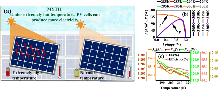 |
| | Fig. 6 (a) Visual representation of impact of lower and higher temperature (K) on solar cell performance, (b) J–V and P–V characteristics at different device's operating temperature (K), and its effect on (c) Jsc, Voc, Pmax, FF, and efficiency. | |
Fig. 6(c) presents the Jsc, Voc, Pmax, FF, and efficiency, revealing that the Jsc marginally decreases with temperature (from 154.49 at 285 K to 154.27 A m−2 at 320 K), reflecting the dominance of recombination over thermal carrier generation and potential material or interfacial degradation, while Voc and Pmax reduce negligibly at higher temperatures. Similarly, the FF also declines (from 65.02 to 64.71% in range of 285–320 K), due to increased resistive losses in the SnO2 and Cu2Te transport layers, while overall efficiency drops from 12.08 to below 12.00%, driven by reduced Voc, Pmax, and FF.59,60 These trends highlight the sensitivity of CH3NH3GeI3-based solar cells to temperature variations and emphasize the need for effective thermal management to maintain optimal performance. The effect of temperature on output characteristics of 1D SnO2/CH3NH3GeI3/Cu2Te solar cell is summarized numerically in Table 10.
Table 10 The effect of device's operating temperature on output characteristics of 1D SnO2/CH3NH3GeI3/Cu2Te solar cell
| Temperature (K) |
Jsc (A m−2) |
Voc (V) |
Pmax (W) |
FF (%) |
Efficiency (%) |
| 285 |
154.49 |
1.203 |
120.85 |
65.02504 |
12.085 |
| 290 |
154.43 |
1.202 |
120.78 |
65.06672 |
12.078 |
| 295 |
154.34 |
1.201 |
120.52 |
65.01860 |
12.052 |
| 300 |
154.25 |
1.200 |
120.45 |
65.07293 |
12.045 |
| 305 |
154.33 |
1.200 |
120.33 |
64.97441 |
12.033 |
| 310 |
154.20 |
1.197 |
120.20 |
65.12173 |
12.020 |
| 315 |
154.26 |
1.201 |
120.05 |
64.79863 |
12.005 |
| 320 |
154.27 |
1.201 |
119.90 |
64.71347 |
11.990 |
This study simulated key parameters—layer thicknesses, doping concentrations, carrier lifetimes, and temperature variations—to optimize the performance of a PVK solar cell. The thickness of ETL, PVK, and HTL layers was systematically varied to balance light absorption, charge transport, and recombination losses; overly thick ETL/HTL layers can increase series resistance and reduce efficiency. Doping concentration were adjusted to fine-tune the built-in electric field, improve energy level alignment, and enhance carrier extraction. Carrier lifetime was analyzed as a measure of recombination, with longer lifetimes indicating better charge collection and fewer losses due to trap-assisted recombination. Simulating a range of lifetimes also provided insights into how defect densities affect device efficiency. Temperature variations were considered to reflect real-world conditions, as elevated temperatures increase recombination and internal resistance, degrading performance. A narrow realistic temperature range was chosen to evaluate thermal stability without extending beyond the intended scope of the study.
CH3NH3GeI3 is a promising lead-free perovskite, but its performance is currently limited by sub-optimal band alignment, high defect densities, and degradation due to moisture sensitivity of Ge-based materials. These issues lead to reduced charge extraction, increased recombination, and compromised long-term stability. Additionally, fabrication challenges, particularly in interface engineering, hinder consistent device optimization.
4. Conclusion
The escalating global challenges of climate change and dependence on environmentally hazardous energy sources have catalyzed the pursuit of sustainable and eco-friendly energy solutions. Among these, solar energy has emerged as a highly efficient, and over the past decades, extensive research has focused on developing advanced materials. In this regard, organic in-organic hybrid perovskite (PVK) materials, particularly CH3NH3GeI3, have garnered substantial interest as absorber layers due to their exceptional multifunctional properties. For this PVK material, using COMSOL, the 1D SnO2/CH3NH3GeI3/Cu2Te solar cell is simulated. The study revealed that performance of solar cell is critically influenced by the thicknesses of electron transport layer (ETL), PVK layer, and hole transport layer (HTL), as well as by doping concentrations, carrier lifetimes, and device's operating temperature. Thinner ETLs (∼10 nm) yield higher current densities, enhanced power output, and superior efficiency, whereas thicker ETLs exhibit diminishing performance. Similarly, the PVK layer achieves optimal performance at ∼700 nm, balancing photon absorption and charge collection efficiency, with efficiency declining beyond thickness. Specifically, open-circuit voltage (Voc) enhances as the PVK layer's thickness increases due to quasi-Fermi level splitting, expressing the direct relation between Voc and quasi-Fermi level splitting. Moreover, HTL thicknesses near 10 nm facilitate effective hole transport with minimal resistive losses, maintaining stable power and efficiency, while thicker HTLs (∼90 nm) introduce minor performance declines. Furthermore, adjustments in acceptor and donor concentrations (NA, ND) significantly influence carrier dynamics, with higher NA enhancing short-circuit current density (Jsc), Voc, and efficiency, whereas higher donor densities stabilize performance but induce saturation trends in Jsc and Voc. Additionally, extending electron–hole (e–h) lifetimes from 1–1000 ns markedly improves Jsc, Voc, and power output (Pmax). Finally, the overall performance including Jsc, Voc, Pmax, fill factor, and efficiency reduce as temperature increases (285–320 K). This study aids for optimizing material properties and device parameters for experimental purposes and encourages the potential of CH3NH3GeI3-based perovskite materials as potential candidates for next-generation photovoltaic applications.
Data availability
The data will be available on request.
Conflicts of interest
The authors declare that there are no financial or any other conflicts of interests.
Acknowledgements
The authors would like to acknowledge the Researchers Supporting Project number (RSP2025R71), King Saud University, Riyadh, Saudi Arabia.
References
- J. Li, M. Irfan, S. Samad, B. Ali, Y. Zhang, D. Badulescu and A. Badulescu, The relationship between energy consumption, CO2 emissions, economic growth, and health indicators, Int. Res. J. Publ. Environ. Health, 2023, 20(3), 2325 Search PubMed.
- W. F. Lamb, T. Wiedmann, J. Pongratz, R. Andrew, M. Crippa, J. G. Olivier, D. Wiedenhofer, G. Mattioli, A. A. Khourdajie, J. House, S. Pachauri, M. Figueroa, Y. Saheb, R. Slade, K. Haubacek, L. Sun, S. K. Ribeiro, S. Khennas, S. D. L. R. D. Can, L. Chapungu, S. J. Davis, I. Bashmakov, H. Dai, S. Dhakal, T. Tan, Y. Geng, B. Gu and J. Minx, A review of trends and drivers of greenhouse gas emissions by sector from 1990 to 2018, Environ. Res. Lett., 2021, 16(7), 073005 Search PubMed.
- R. Prăvălie, I. Sîrodoev, J. Ruiz-Arias and M. Dumitraşcu, Using renewable (solar) energy as a sustainable management pathway of lands highly sensitive to degradation in Romania. A countrywide analysis based on exploring the geographical and technical solar potentials, Renewable Energy, 2022, 193, 976–990 Search PubMed.
- D. Bogdanov, A. Gulagi, M. Fasihi and C. Breyer, Full energy sector transition towards 100% renewable energy supply: Integrating power, heat, transport and industry sectors including desalination, Appl. Energy, 2021, 283, 116273 Search PubMed.
- K. Ahmad, M. Q. Khan and H. Kim, Simulation and fabrication of all-inorganic antimony halide perovskite-like material based Pb-free perovskite solar cells, Opt. Mater., 2022, 128, 112374 Search PubMed.
- Y. Zhao, J. Zhu, B. He and Q. Tang, Dimensionality control of SnO2 films for hysteresis-free, all-inorganic CsPbBr3 perovskite solar cells with efficiency exceeding 10%, ACS Appl. Mater. Interfaces, 2021, 13(9), 11058–11066 Search PubMed.
- G. Ding, Y. Zheng, X. Xiao, H. Cheng, G. Zhang, Y. Shi and Y. Shao, Sustainable development of perovskite solar cells: keeping a balance between toxicity and efficiency, J. Mater. Chem. A, 2022, 10(15), 8159–8171 Search PubMed.
- S. Ullah, M. F. U. Din, J. Khan Kasi, A. Khan Kasi, K. Vegso, M. Kotlar, K. Micsuik, M. Jergel, V. Nadazdy, P. Siffalovic, E. Majkova and A. Fakharuddin, Mesoporous SnO2 nanoparticle-based electron transport layer for perovskite solar cells, ACS Appl. Nano Mater., 2022, 5(6), 7822–7830 Search PubMed.
- S. T. Jan and M. Noman, Exploring the potential of MAGeI3 perovskite cells with novel charge transport material optimization, Optik, 2024, 301, 171684 Search PubMed.
- S. Guang, J. Yu, H. Wang, X. Liu, S. Qu, R. Zhu and W. Tang, A low temperature processable tin oxide interlayer via amine-modification for efficient and stable organic solar cells, J. Energy Chem., 2021, 56, 496–503 Search PubMed.
- P. Sakthivel, S. Foo, M. Thambidurai, P. C. Harikesh, N. Mathews, R. Yuvakkumar, G. Ravi and C. Dang, Efficient and stable planar perovskite solar cells using co-doped tin oxide as the electron transport layer, J. Power Sources, 2020, 471, 228443 Search PubMed.
- K. Bhavsar and P. B. Lapsiwala, Numerical simulation of perovskite solar cell with different material as electron transport layer using SCAPS-1D software, Semicond. Phys. Quantum Electron. Optoelectron., 2021, 24(3), 341–347 Search PubMed.
- A. Uddin and H. Yi, Progress and challenges of SnO2 electron transport layer for perovskite solar cells: A critical review, Sol. RRL, 2022, 6(6), 2100983 Search PubMed.
- M. E. A. Boudia, Q. Wang and C. Zhao, Simulation and Comparison of the Photovoltaic Performance of Conventional and Inverted Organic Solar Cells with SnO2 as Electron Transport Layers, Energies, 2024, 17(13), 3302 Search PubMed.
- M. Singh, A. Ng, Z. Ren, H. Hu, H. C. Lin, C. W. Chu and G. Li, Facile synthesis of composite tin oxide nanostructures for high-performance planar perovskite solar cells, Nano Energy, 2019, 60, 275–284 Search PubMed.
- Z. Xu, S. H. Teo, L. Gao, Z. Guo, Y. Kamata, S. Hayase and T. Ma, La-doped SnO2 as ETL for efficient planar-structure hybrid perovskite solar cells, Org. Electron., 2019, 73, 62–68 Search PubMed.
- H. Yi, D. Wang, M. A. Mahmud, F. Haque, M. B. Upama, C. Xu, L. Duan and A. Uddin, Bilayer SnO2 as electron transport layer for highly efficient perovskite solar cells, ACS Appl. Energy Mater., 2018, 1(11), 6027–6039 Search PubMed.
- N. Singh, A. Agarwal and M. Agarwal, Numerical simulation of highly efficient lead-free perovskite layers for the application of all-perovskite multi-junction solar cell, Superlattices Microstruct., 2021, 149, 106750 Search PubMed.
- H. Abdulsalam and G. Babaji, First principle study on lead-free CH3NH3GeI3 and CH3NH3GeBr3 perovskite solar cell using FHI-aims code, J. Found. Appl. Phys., 2019, 6(1), 76–88 Search PubMed.
- A. A. Kanoun, M. B. Kanoun, A. E. Merad and S. Goumri-Said, Toward development of high-performance perovskite solar cells based on CH3NH3GeI3 using computational approach, Sol. Energy, 2019, 182, 237–244 Search PubMed.
- Y. Q. Zhao, B. Liu, Z. L. Yu, J. Ma, Q. Wan, P. B. He and M. Q. Cai, Strong ferroelectric polarization of CH3NH3GeI3 with high-absorption and mobility transport anisotropy: theoretical study, J. Mater. Chem. C, 2017, 5(22), 5356–5364 Search PubMed.
- Y. Jiao, Y. Lv, J. Li, M. Niu and Z. Yang, Exploring electronic and optical properties of CH3NH3GeI3 perovskite: Insights from the first principles, J. Comput. Theor. Chem., 2017, 1114, 20–24 Search PubMed.
- Y. Liu, The development of low toxic and high efficient solar cells, J. Phys.: Conf. Ser., 2020, 1653(1), 012002 Search PubMed.
- C. C. Stoumpos, L. Frazer, D. J. Clark, Y. S. Kim, S. H. Rhim, A. J. Freeman, J. B. Katterson, J. I. Jang and M. G. Kanatzidis, Hybrid germanium iodide perovskite semiconductors: active lone pairs, structural distortions, direct and indirect energy gaps, and strong nonlinear optical properties, J. Am. Chem. Soc., 2015, 137(21), 6804–6819 Search PubMed.
- S. Bhattarai and T. D. Das, Optimization of carrier transport materials for the performance enhancement of the MAGeI3 based perovskite solar cell, Sol. Energy, 2021, 217, 200–207 Search PubMed.
- H. Kuang and Y. Xiao, Numerical simulation of Cu2Te based thin film solar cell with Cu2O HTL for high efficiency, Micro Nanostruct., 2024, 188, 207790 Search PubMed.
- K. Chakraborty, N. R. Medikondu, P. B. Kanakavalli, V. V. Kamesh, S. Das, M. G. Choudhury and S. Paul, Comparative study of structural, opto-electronic properties of Cs2TiX6-based single halide double perovskite solar cells: computational and experimental approach, Phys. Scr., 2024, 99(10), 105554 Search PubMed.
- N. Kushwah, G. Kedarnath, A. Wadawale, K. K. Halankar, B. P. Mandal, M. Jafar and B. Vishwanadh, Molecular Precursor-Driven Synthesis of Copper Telluride Nanostructures for LIB Anode Application, Inorg. Chem., 2023, 62(23), 8823–8834 Search PubMed.
- S. R. Al Ahmed, M. Rahaman, A. Sunny, S. Rahman, M. S. Islam, T. A. E. M. Taha, Z. A. Alrowaili and M. S. Mian, Enhancing the efficiency of Cu2Te thin-film solar cell with WS2 buffer layer: a simulation study, Opt Laser. Technol., 2023, 159, 108942 Search PubMed.
- W. Henni, W. L. Rahal, G. I. Toki, M. K. Mohammed, L. B. Farhat, S. Ezzine, R. Pandey, A. Boukkortt and M. K. Hossain, Effect of adding Cu2O as a back surface field layer on the performance of copper manganese tin sulfide solar cells, Sustainability, 2023, 15(19), 14322 Search PubMed.
- R. Stangl, C. Leendertz and J. Haschke, Numerical simulation of solar cells and solar cell characterization methods: the open-source on demand program AFORS-HET, Sol. Energy, 2010, 14, 319–352 Search PubMed.
- Y. Zhou and A. Gray-Weale, A numerical model for charge transport and energy conversion of perovskite solar cells, Phys. Chem. Chem. Phys., 2016, 18(6), 4476–4486 Search PubMed.
- P. J. Manga, M. Maina, H. Samaila, E. W. Likta, R. O. Amusat and S. Daniel, Exploring the structural mechanics of titanium nickel solid alloy using COMSOL Multiphysics: A Poisson equation and continuity equation perspective, Sci. World J., 2024, 19(1), 71–77 Search PubMed.
- A. Bablich, M. Müller, R. Bornemann, A. Nachtigal and P. Haring Bolívar, High responsivity and ultra-low detection limits in nonlinear a-Si: H pin photodiodes enabled by photogating, Photonic Sens., 2023, 13(4), 230415 Search PubMed.
- F. Brioua, C. Daoudi, B. Mekimah and B. Lekouaghet, The impact of a ZnO space layer on enhancing the efficiency of P3HT: PCBM blend-based organic solar cells, Phys. Scr., 2024, 99(8), 085951 Search PubMed.
- H. Asghar, T. Riaz, H. A. Mannan, S. M. Khan and O. M. Butt, Rheology and modeling insights into dye-sensitized solar cells (DSSCs) material: Bridging the gap to solar energy advancements, Renew. Sustain. Energy Rev., 2024, 193, 114298 Search PubMed.
- Z. Varga and E. Racz, Application development with finite element method to calculate photogeneration rate and open-circuit voltage of dye sensitized solar cell, Theory Comput. Syst., 2022, 2(2), 17–24 Search PubMed.
- T. Nakamura, W. Yanwachirakul, M. Imaizumi, M. Sugiyama, H. Akiyama and Y. Okada, Reducing Shockley–Read–Hall recombination losses in the depletion region of a solar cell by using a wide-gap emitter layer, J. Appl. Phys., 2021, 130, 153102 Search PubMed.
- A. Fell, T. Niewelt, B. Steinhauser, F. D. Heinz, M. C. Schubert and S. W. Glunz, Radiative recombination in silicon photovoltaics: Modeling the influence of charge carrier densities and photon recycling, Sol. Energy Mater. Sol. Cells, 2021, 230, 111198 Search PubMed.
- Á. Nagy, I. Bodnár and E. Kovács, Simulation of the Thermal Behavior of a Photovoltaic Solar Panel Using Recent Explicit Numerical Methods, Theor. Comput. Syst., 2024, 7(7), 2400089 Search PubMed.
- M. Q. Kareem, S. A. Hassan, S. S. Alimardan, S. M. Shareef and M. M. Ameen, CHTS/Zn2P3-based solar cells with enhanced efficiency through ETL engineering: A numerical study, J. Phys. Chem. Solids, 2024, 188, 111931 Search PubMed.
- G. Pindolia, S. M. Shinde and P. K. Jha, Optimization of an inorganic lead free RbGeI3 based perovskite solar cell by SCAPS-1D simulation, Sol. Energy, 2022, 236, 802–821 Search PubMed.
- S. Sakib, M. Y. M. Noor, M. R. Salim, A. S. Abdullah, A. I. Azmi, M. H. Ibrahim and M. H. Ibrahim, Effect of transport layer thickness in lead-based perovskite solar cell: A numerical simulation, Mater. Today: Proc., 2023, 80, 1022–1026 Search PubMed.
- A. Bag, R. Radhakrishnan, R. Nekovei and R. Jeyakumar, Effect of absorber layer, hole transport layer thicknesses, and its doping density on the performance of perovskite solar cells by device simulation, Sol. Energy, 2020, 196, 177–182 Search PubMed.
- A. Mortadi, E. El Hafidi, M. Monkade and R. El Moznine, Investigating the influence of absorber layer thickness on the performance of perovskite solar cells: a combined simulation and impedance spectroscopy study, Mater. Sci. Energy Technol., 2024, 7, 158–165 Search PubMed.
- A. Ahmed, K. Riaz, H. Mehmood, T. Tauqeer and Z. Ahmad, Performance optimization of CH3NH3Pb(I1-xBrx)3 based perovskite solar cells by comparing different ETL materials through conduction band offset engineering, Opt. Mater., 2020, 105, 109897 Search PubMed.
- B. K. Ravidas, A. R. Kumar, A. Praveen, S. K. Agnihotri, S. Bhattarai, R. Pandey, J. Madan, S. Singh, M. K. Hossain, M. K. Roy and D. P. Samajdar, Integration of SCAPS-1D and density functional theory for the performance evaluation of RbGeI3-based perovskite solar cell, J. Phys. Chem. Solids, 2025, 196, 112325 Search PubMed.
- R. Ranjan, N. Anand, M. N. Tripathi, N. Srivastava, A. K. Sharma, M. Yoshimura, L. Chang and R. N. Tiwari, SCAPS study on the effect of various hole transport layer on highly efficient 31.86% eco-friendly CZTS based solar cell, Sci. Rep., 2023, 13(1), 18411 Search PubMed.
- M. Mottakin, D. K. Sarkar, V. Selvanathan, M. J. Rashid, K. Sobayel, A. M. Hasan, M. A. Islam, G. Muhammad, M. Shahiduzzaman and M. Akhtaruzzaman, Photoelectric performance of environmentally benign Cs2TiBr6-based perovskite solar cell using spinel NiCo2O4 as HTL, Optik, 2023, 272, 170232 Search PubMed.
- S. T. Jan and M. Noman, Influence of layer thickness, defect density, doping concentration, interface defects, work function, working temperature and reflecting coating on lead-free perovskite solar cell, Sol. Energy, 2022, 237, 29–43 Search PubMed.
- S. A. Dar and B. S. Sengar, Analytical modeling and numerical investigation of grain size effects on polycrystalline perovskite based Thin-Film solar Cells: Performance insights and implications, Sol. Energy, 2025, 289, 113313 Search PubMed.
- T. Kirchartz, High open-circuit voltages in lead-halide perovskite solar cells: experiment, theory and open questions, Philos. Trans. R. Soc., A, 2019, 377(2152), 20180286 Search PubMed.
- A. Sachenko, V. Kostylyov and M. Evstigneev, Space charge region recombination in highly efficient silicon solar cells, Semicond. Phys. Quantum Electron. Optoelectron., 2024, 27(1), 010–027 Search PubMed.
- Q. Wang, S. Shao, B. Xu, H. Duim, J. Dong, S. Adjokatse, G. Portale, J. Hou, M. Saba and M. A. Loi, Impact of the hole transport layer on the charge extraction of Ruddlesden–Popper perovskite solar cells, ACS Appl. Mater. Interfaces, 2020, 12(26), 29505–29512 Search PubMed.
- V. S. Chirvony, K. S. Sekerbayev, D. Perez-del-Rey, J. P. Martinez-Pastor, F. Palazon, P. P. Boix, T. I. Taurbayev, M. Sessolo and H. J. Bolink, Short photoluminescence lifetimes in vacuum-deposited CH3NH3PbI3 perovskite thin films as a result of fast diffusion of photogenerated charge carriers, J. Phys. Chem. Lett., 2019, 10(17), 5167–5172 Search PubMed.
- S. Akel, A. Kulkarni, U. Rau and T. Kirchartz, Relevance of long diffusion lengths for efficient halide perovskite solar cells, Phys. Rev. X Energy, 2023, 2(1), 013004 Search PubMed.
- I. Gulomova, O. Accouche, R. Aliev, Z. Al Barakeh and V. Abduazimov, Optimizing geometry and ETL materials for high-performance inverted perovskite solar cells by TCAD simulation, Nanomaterials, 2024, 14(15), 1301 Search PubMed.
- A. Ren, H. Lai, X. Hao, Z. Tang, H. Xu, B. M. F. Y. Jeco, K. Watenabe, J. Zhang, M. Sugiyama, J. Wu and D. Zhao, Efficient perovskite solar modules with minimized nonradiative recombination and local carrier transport losses, Joule, 2020, 4(6), 1263–1277 Search PubMed.
- D. Sahoo and N. B. Manik, Study on the effect of temperature on electrical and photovoltaic parameters of lead-free tin-based Perovskite solar cell, Indian J. Phys., 2023, 97(2), 447–455 Search PubMed.
- M. K. Hossain, M. A. Islam, M. S. Uddin, P. Paramasivam, J. A. Hamid, R. A. Alshgari, V. K. Mishra and R. Haldhar, Design and simulation of CsPb.625Zn.375IBr2-based perovskite solar cells with different charge transport layers for efficiency enhancement, Sci. Rep., 2024, 14(1), 1–22 Search PubMed.
|
| This journal is © The Royal Society of Chemistry 2025 |
Click here to see how this site uses Cookies. View our privacy policy here. 
 Open Access Article
 This Open Access Article is licensed under a Creative Commons Attribution-Non Commercial 3.0 Unported Licence
 a,
Muhammad Mehaka,
Umair Alia,
Ghulam Moin U Dina,
Shahid M. Ramayb,
M. Younisc and
Shahid Atiq
a,
Muhammad Mehaka,
Umair Alia,
Ghulam Moin U Dina,
Shahid M. Ramayb,
M. Younisc and
Shahid Atiq