
 Open Access Article
 This Open Access Article is licensed under a
 Creative Commons Attribution 3.0 Unported Licence
Perovskite photodetectors prepared by flash evaporation printing†
Haoming Weiab,
He Mac,
Meiqian Taib,
Yang Wei *a,
Dongqi Lia,
Xingyue Zhaob,
Hong Lin*b,
Shoushan Fanabd and
Kaili Jiang*ad
*a,
Dongqi Lia,
Xingyue Zhaob,
Hong Lin*b,
Shoushan Fanabd and
Kaili Jiang*ad
aState Key Laboratory of Low-Dimensional Quantum Physics, Department of Physics, Tsinghua-Foxconn Nanotechnology Research Center, Tsinghua University, Beijing 100084, China. E-mail: WeiYang@tsinghua.edu.cn
bState Key Laboratory of New Ceramics and Fine Processing, School of Materials Science and Engineering, Tsinghua University, Beijing 100084, China. E-mail: hong-lin@tsinghua.edu.cn
cCollege of Applied Sciences, Beijing University of Technology, Beijing 100124, China
dCollaborative Innovation Center of Quantum Matter, Beijing 100084, China. E-mail: JiangKL@tsinghua.edu.cn
First published on 11th July 2017
Abstract
Organometallic halide perovskites have expanded promising approaches for fabricating optoelectronic devices with low cost and high performance since their discovery. Here we propose a novel technique, flash evaporation printing, to prepare perovskite thin films with high quality in an efficient way, whose success is attributed to freestanding carbon nanotube films serving as the flash evaporator. It is convenient to print patterned perovskites using this method due to the compact deposition geometry. The patterned perovskite thin films were further manufactured to planar-type photodetectors, and the performance of the photoelectric devices was evaluated. The as-prepared photodetector shows a considerable peak responsivity and fast temporal response, proving flash evaporation printing an effective route for exploiting high-performance perovskite photodetectors, and this technique can find potential applications in more fields.
Organic–inorganic hybrid perovskites, such as CH3NH3PbX3 (X = Cl, Br, I), have recently captured much attention due to their unique electrical and optical properties, which provides promising routes for fabricating optoelectronic devices with high performance at low cost.1–10 Quintessentially, perovskite thin films can be synthesized by various deposition procedures including simple one-step solution coating,1,11,12 sequential dip coating,13 vapour phase deposition14 and combinations thereof.15 Among these methods, dual source vapour deposition has been developed as a reliable technique to fabricate perovskite thin films and photovoltaic cells with high efficiency.14,16 Physical vapor deposition (PVD) methodology has shown its potential on quality and purity control, taking advantage of the intrinsic high purity of sublimated compounds. Besides, this technique allows for the further integration of perovskite thin film with other functional thin films, as it is inherited from standard thin film technology. However, it is a challenge to balance the organic and inorganic deposition rates, since the organic salt generally does not evaporate as a molecular species, but rather dissociates into the free organic amine and hydrogen halide gas.17 Moreover, the conventional PVD method does not have the cost advantage due to the facility and the process.
In this study, we developed a flash evaporation printing (FEP) technique to prepare high-quality thin films of CH3NH3PbI3 (MAPbI3) perovskite, which inherits the merits of PVD process and addresses its shortcomings as well. A cross-stacked superaligned carbon nanotube (CNT) film was employed as a flash evaporator for their ultrasmall heat capacity per unit area and fast thermal response ability.18–20 A flash evaporation transfer ribbon was then developed by coating MAPbI3 on the CNT evaporator. The transfer ribbon can be rapidly heated by sweeping laser beam on it, triggering a flash evaporation of MAPbI3. A MAPbI3 perovskite thin film with high quality was successfully printed on the substrate by the gas phase transportation process from the hot CNTs to the cold substrate. Planar-type photodetectors were further fabricated by printing the perovskite thin films on Au interdigital electrodes. The photodetectors were found sensitive to a broadband response spectrum in visible light, showing a high responsivity (R) of 4.98 A W−1, 2.56 A W−1 at 460 nm and 694 nm under a bias voltage of 5 V, respectively. Additionally, the as-prepared photodetectors showed a high response speed. The single evaporating source makes the FEP more simplified than the dual sources process, as it avoids the difficulties in accurate control of deposition rate and precursors ratio in customary vacuum evaporation.21 The FEP technique also simplifies the complicated thin film deposition facility into a compact printing module by using a CNT evaporator, which will have a significant cost advantage. The FEP technique has proven itself applicable to miscellaneous materials, and will be a promising candidate in printable electronics and flexible electronics.
CNT films used in this work were dry spun from superaligned CNT arrays synthesized on silicon wafers by a low-pressure chemical vapor deposition (LPCVD) method.22,23 A cross-stacked CNT sheet with 15 single layers was coated onto a 25 × 25 mm2 metal frame. After the stacking process, the CNT sheet was dipped in ethanol solvent and dried in air at room temperature to make CNTs firmly compact together, such a CNT sheet was the flash evaporator of the FEP technique. The perovskite precursor solution was consisted of 1 M PbI2 and 2.2 M CH3NH3I (MAI) in anhydrous solvent of dimethylformamide (DMF). Perovskite precursor solution of 100 μL was then dropped and subsequently spin-coated on the CNT sheet at 2000 rpm for 30 seconds. The transfer ribbon with MAPbI3 precursor was thus made after removing the solvents by annealing the composite film at 100 °C for 10 minutes. The scanning electron microscopy (SEM) image of the transfer ribbon is shown in the left panel of Fig. 1 inset.
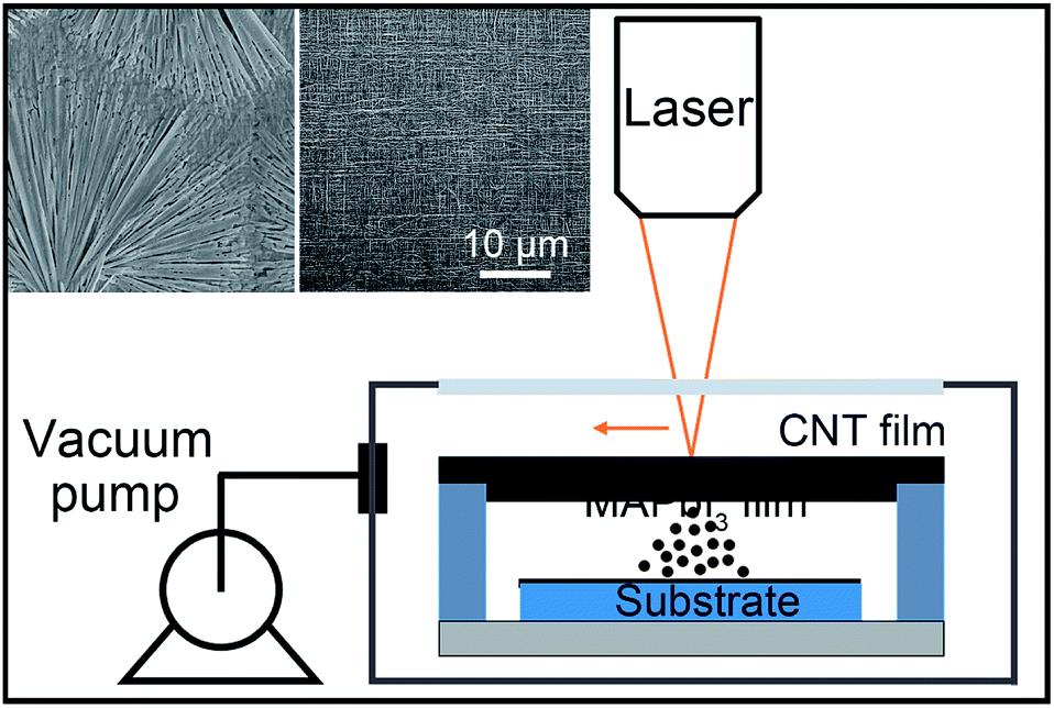 | ||
| Fig. 1 Schematic depiction of the experimental setup of FEP. The inset are SEM images of the MAPbI3 transfer ribbon surface (left) and the clean CNT evaporator after flash evaporation (right). | ||
The FEP technology is sketched in Fig. 1. The flash evaporation transfer ribbon with MAPbI3 was set on top of a substrate with a 1 mm gap, and the base pressure of the process chamber was ∼10−3 mbar. This compact geometry of the FEP simplifies the process chamber and is more cost effective than conventional evaporation facilities. The close distance between the source and the substrate can efficiently improve the material utilization during evaporation and thus effectively reduce lead pollution to the environment. As there is no significant change of the film quality when modulating the source-substrate distance from 1 to 3 mm (Fig. S1†), the 1 mm gap was employed to achieve a more compact structure. A scanning yttrium aluminum garnet (YAG) laser was introduced on the suspended transfer ribbon in the vacuum chamber through a quartz window. The wavelength of the laser was 1.06 μm, and the power output was optimized to be 12 W. The laser spot, which was ∼1 mm in diameter, scanned on the CNT film along parallel lines with a pitch of 100 μm. The scanning speed was 1 m s−1 in our experiments. The CNT evaporator can be heated to about 1100 °C instantaneously by the laser beam irradiation due to its ultrasmall heat capacity. The hot CNT film caused the flash evaporation immediately and the perovskite precursor on the CNT evaporator is transfer printed onto the substrate via the vapour phase transportation process. It takes only about 4 seconds to print a 20 × 20 mm2 perovskite film. The right panel of Fig. 1 inset shows the morphology of a transfer ribbon after flash evaporation, the clean surface without any residue suggests that the FEP is efficient.
The surface morphology of the as-printed perovskite film was investigated by SEM. The SEM image in Fig. 2a shows a typical morphology of the as-prepared perovskite thin film, indicating a high coverage. The grain size of the perovskite film was counted carefully for statistical analysis, and the crystallite size distribution is given in Fig. S2.† The mean size of the 258 crystalline grains counted is 280 nm according to the statistics, and the sizes of most particles are over 200 nm, accounting for more than 70%. The crystalline structure was further studied by X-ray diffraction (XRD) and the result is depicted in Fig. 2b. Intense diffraction peaks at 14.1°, 28.4°, and 31.8° of the curve could be assigned to (110), (220), and (310) planes of tetragonal MAPbI3 phase.4,13,14 Moreover, the XRD pattern of MAPbI3 prepared using our FEP technique exhibits two extra peaks at 19.9° and 24.4°, which were observed in the simulated perovskite XRD pattern reported by Graetzel et al.16 Besides, in the region of the (110) diffraction peak, there is barely signature of the diffraction peak for PbI2. All these analytical results indicate that a high level of film quality and phase purity can be acquired by the FEP methodology. In addition, the ultraviolet-visible (UV-vis) spectroscopy was used to study the characteristic absorption of the perovskite films, which is given in Fig. 2c. It shows a band-to-band optical absorption edge at ∼800 nm (∼1.55 eV) for MAPbI3 perovskite, with an absorption plateau at wavelengths below 500 nm.6,24 The strong absorption of light indicates the perovskite film's possible photoelectric applications.
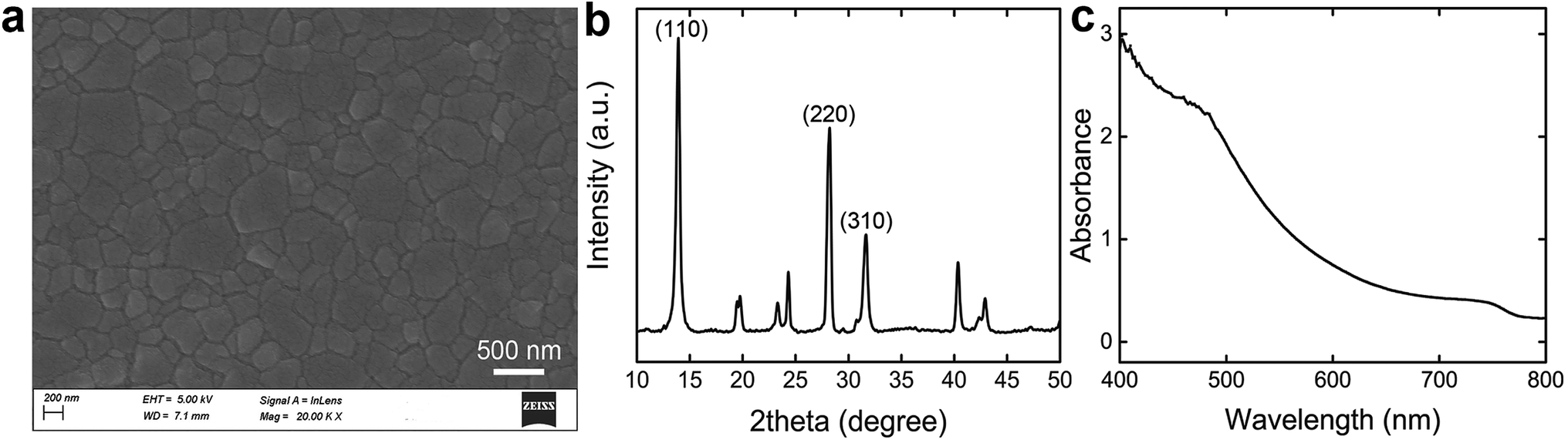 | ||
| Fig. 2 Characterization of the as-printed thin films. (a) SEM image and (b) XRD pattern and (c) UV-vis absorption spectrum of the perovskite thin films deposited on FTO substrates. | ||
The FEP technique was further employed to fabricate planar-type perovskite photodetectors. The fabrication procedures are illustrated in Fig. 3a. An array of interdigital gold electrodes was first deposited on the SiO2/Si wafer by conventional photolithography and e-beam evaporation process. The gap between Au electrodes was 20 μm. A perforated metal mask was then covered on the substrate and their patterns were aligned each other under an optical microscope. A central 500 × 500 μm2 square of each element was thus exposed for the perovskite thin film printing, as shown in the middle panel of Fig. 3a. After the FEP of perovskite thin film, an array of the planar-type photodetectors was successfully fabricated on the substrate. The effective illuminated area of MAPbI3 in each element was about 2.5 × 10⁻⁷ m2. The optical micrographs in Fig. 3b correspond to the three cartoons sketched in Fig. 3a, respectively. Moreover, the success in photodetector array fabrication also tells that the FEP technique is compatible with conventional semiconducting procedures, and it is also competent to print patterned thin films with a shadow mask strategy, which is essential for practical applications of a new printing methodology.
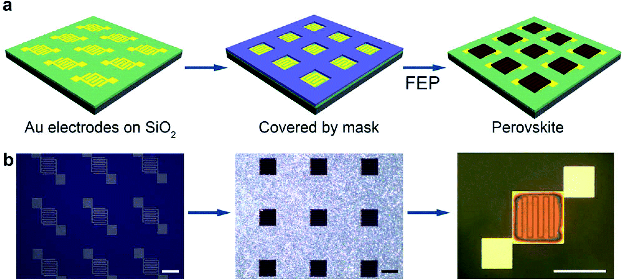 | ||
| Fig. 3 (a) Schematic illustration of the as-fabricated perovskite photodetectors. (b) Optical micrographs of the gold interdigital fingers, the perforated metal mask and the as-fabricated photodetector element. The scale bar is 500 μm. | ||
The photoelectric convertibility of the as-fabricated perovskite photodetectors was studied under the illumination via an optical microscope of a probe station. A 633 nm laser was first employed as the light source with the optical power densities varying from 4.79 to 32.99 mW cm−2. The light intensities were measured with a calibrated power meter (Thorlabs PM100D). A bias was applied across the two pads of the device and I–V curves under altered illumination power were plotted by Agilent B2902A sourcemeter. An applied voltage bias can provide the local electric field for the MAPbI3 perovskite film, leading to separate the photo-generated electrons and holes and decrease the electron–hole recombination rates, which is crucial for the high gain of the photodetector. After carriers dissociate, the electrons would migrate to the conduction band of MAPbI3 and further to the electrode with positive potential, while the holes would flow to the valence band and further to the electrode with negative potential. All measurements were performed in air at room temperature. The results are shown in Fig. 4a, in which the current density was defined as ratio of the current to the effective area of the device. The dark current was plotted as a reference (the black curve), which was as low as 0.75 nA at 5 V bias. The dark resistance is about 6700 MΩ. When the device was exposed to light, the photocurrent increased significantly. The I–V curves show an almost linear and symmetrical behavior, indicating a well-symmetrical internal structure of the device, and the bright resistance at 32.99 mW cm−2 derived from the I–V curves is 0.1 MΩ. The I–V characteristics of sandwiched cell consisting of fluorine-doped tin oxide (FTO)-coated glass/MAPbI3 thin film/Au device were also measured, as shown in Fig. S3.† The DC (direct current) conductivity (σ0) can be determined from the slope of the I–V plot, I = σ0Ad−1V,25 where A is area of sample (0.26 cm2) and d is the thickness of the sample (∼300 nm). The determined conductivity was 0.0065 mS cm−1.
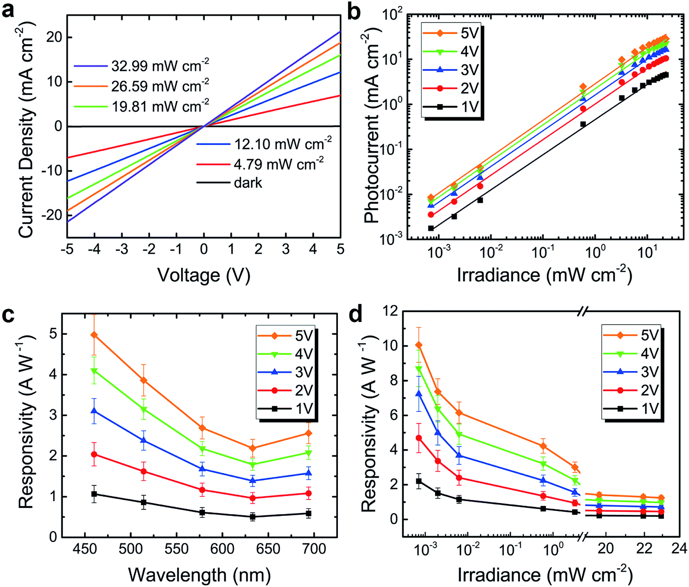 | ||
| Fig. 4 (a) Photocurrent versus voltage curves under different irradiation densities. (b) Photocurrent linearity upon varying the 633 nm input irradiance at various bias. (c) Spectral responsivity of the as-fabricated device illuminated by bandpass-filtered light from Xe lamp. (d) Responsivity dependence on input irradiance at 633 nm with various bias. | ||
The irradiance-dependent photocurrents at different bias were further plotted in Fig. 4b and fitted linearly, revealing a linear response across ∼4 orders of intensity. The linear dynamic range (LDR, typically quoted in dB) can be calculated by the equation:
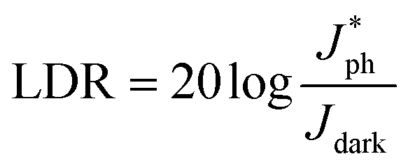
 is the photocurrent measured at a light intensity of 1 mW cm−2.26 The calculated linear dynamic range (LDR) is ∼80 dB, which is higher than InGaAs photodetectors (66 dB).
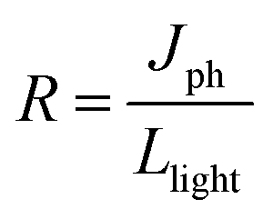
Responsivity (R), the ratio of photocurrent to the incident light intensity, can be expressed by:
To further investigate the temporal response of the photodetector, a supercontinuum white light source was employed as a modulated illumination.31 The pulse duration of the light source was less than 2 ns and the frequency was set at 5000 Hz. The transient photocurrent response of the device was recorded by an oscilloscope and shown in Fig. 5a. One of the transient signals was presented in Fig. 5b to further characterize the rise time and fall time. The rise time was defined as the time to transition between 10% of the maximum photocurrent to 90% of the maximum photocurrent; the fall time was from 90% down to 10%. The rise time and the fall time of the photodetector were around 6.1 and 17.6 μs, respectively. The decay rate is slower than the rise rate, which can be typically attributed to the diffusive contribution to photocurrent during discharging.32 The temporal response presented here are faster than some organic, quantum dot and hybrid photodetectors in the literature,33–38 which can naturally extend the scope of device applications and reveal the great potentials of the as-developed FEP methodology.
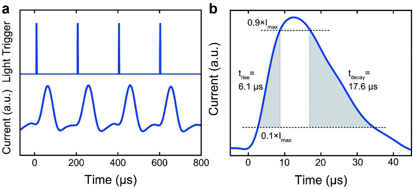 | ||
| Fig. 5 Perovskite photodetector speed at zero bias. (a) Transient current output of the device to a time-varying incident light signal. (b) Photocurrent rise and decay. | ||
Conclusions
To conclude, by utilizing superaligned CNT films with ultrasmall heat capacity and fast thermal response as the flash evaporator, a convenient FEP technology was developed and used to print perovskite thin films with high quality. The as-prepared films' property and morphology were proved favorable by XRD and SEM. As the FEP technology offers a simple but efficient solution to print patterned thin films, it is employed to prepare perovskite patterns using a shadow mask, and the patterning printing can also be realized by a point-by-point printing thanks to its compact geometry. The patterned perovskite thin films were further fabricated into planar-type photodetectors, and the photoresponse performance of the devices were evaluated. The lowest detectable irradiance power density was evaluated to be 0.71 μW cm−2, under which the highest R values of 10.06 A W−1 at 5 V and 2.20 A W−1 at 1 V were achieved, respectively. The transient photoresponse measurement showed the device had a very fast photoresponse speed, the rise time was 6.1 μs and the fall time was 17.6 μs, faster than some organic, quantum dot and hybrid photodetectors according to the literature. In addition, further enhancements of the photodetector performance may be predictable by improving the interface between the perovskite films and gold electrodes. These results demonstrate that FEP is an effective way for exploiting high-performance perovskite photodetectors, and FEP is also a promising methodology for printing other functional materials, finding its prospective applications in printed electronics, organic electronics and future flexible electronics.Acknowledgements
This work was financially supported by the National Basic Research Program of China (No. 2012CB932301), and the National Natural Science Foundation of China (No. 51472142, 51102147).Notes and references
- M. M. Lee, J. Teuscher, T. Miyasaka, T. N. Murakami and H. J. Snaith, Science, 2012, 338, 643–647 CrossRef CAS PubMed.
- M. A. Loi and J. C. Hummelen, Nat. Mater., 2013, 12, 1087–1089 CAS.
- G. Hodes, Science, 2013, 342, 317–318 CrossRef CAS PubMed.
- J. Y. Jeng, Y. F. Chiang, M. H. Lee, S. R. Peng, T. F. Guo, P. Chen and T. C. Wen, Adv. Mater., 2013, 25, 3727–3732 CrossRef CAS PubMed.
- C. C. Stoumpos, C. D. Malliakas and M. G. Kanatzidis, Inorg. Chem., 2013, 52, 9019–9038 CrossRef CAS PubMed.
- S. D. Stranks, G. E. Eperon, G. Grancini, C. Menelaou, M. J. P. Alcocer, T. Leijtens, L. M. Herz, A. Petrozza and H. J. Snaith, Science, 2013, 342, 341–344 CrossRef CAS PubMed.
- G. Xing, N. Mathews, S. Sun, S. S. Lim, Y. M. Lam, M. Grätzel, S. Mhaisalkar and T. C. Sum, Science, 2013, 342, 344–347 CrossRef CAS PubMed.
- P. Gao, M. Grätzel and M. K. Nazeeruddin, Energy Environ. Sci., 2014, 7, 2448–2463 CAS.
- G. Xing, N. Mathews, S. S. Lim, N. Yantara, X. Liu, D. Sabba, M. Grätzel, S. Mhaisalkar and T. C. Sum, Nat. Mater., 2014, 13, 476–480 CrossRef CAS PubMed.
- H. Zhou, Q. Chen, G. Li, S. Luo, T. B. Song, H. S. Duan, Z. Hong, J. You, Y. Liu and Y. Yang, Science, 2014, 345, 542–546 CrossRef CAS PubMed.
- H. S. Kim, C. R. Lee, J. H. Im, K. B. Lee, T. Moehl, A. Marchioro, S. J. Moon, R. Humphry-Baker, J. O. Yum, J. E. Moser, M. Grätzel and N. G. Park, Sci. Rep., 2012, 2, 591 Search PubMed.
- J. H. Heo, S. H. Im, J. H. Noh, T. N. Mandal, C. S. Lim, J. A. Chang, Y. H. Lee, H. J. Kim, A. Sarkar, M. K. Nazeeruddin, M. Grätzel and S. I. Seok, Nat. Photonics, 2013, 7, 486–491 CrossRef CAS.
- J. Burschka, N. Pellet, S. J. Moon, R. Humphry-Baker, P. Gao, M. K. Nazeeruddin and M. Grätzel, Nature, 2013, 499, 316–319 CrossRef CAS PubMed.
- M. Liu, M. B. Johnston and H. J. Snaith, Nature, 2013, 501, 395–398 CrossRef CAS PubMed.
- Q. Chen, H. Zhou, Z. Hong, S. Luo, H. S. Duan, H. H. Wang, Y. Liu, G. Li and Y. Yang, J. Am. Chem. Soc., 2014, 136, 622–625 CrossRef CAS PubMed.
- O. Malinkiewicz, A. Yella, Y. H. Lee, G. M. Espallargas, M. Graetzel, M. K. Nazeeruddin and H. J. Bolink, Nat. Photonics, 2014, 8, 128–132 CrossRef CAS.
- D. B. Mitzi, M. T. Prikas and K. Chondroudis, Chem. Mater., 1999, 11, 542–544 CrossRef CAS.
- K. Liang, D. B. Mitzi and M. T. Prikas, Chem. Mater., 1998, 10, 403–411 CrossRef CAS.
- L. Xiao, Z. Chen, C. Feng, L. Liu, Z. Bai, Y. Wang, L. Qian, Y. Zhang, Q. Li, K. Jiang and S. Fan, Nano Lett., 2008, 8, 4539–4545 CrossRef CAS PubMed.
- Y. Wei, X. Lin, K. Jiang, P. Liu, Q. Li and S. Fan, Nano Lett., 2013, 13, 4795–4801 CrossRef CAS PubMed.
- H. Wei, Y. Wei, X. Lin, P. Liu, S. Fan and K. Jiang, Nano Lett., 2015, 15, 1843–1848 CrossRef CAS PubMed.
- K. Jiang, Q. Li and S. Fan, Nature, 2002, 419, 801 CrossRef CAS PubMed.
- K. Jiang, J. Wang, Q. Li, L. Liu, C. Liu and S. Fan, Adv. Mater., 2011, 23, 1154–1161 CrossRef CAS PubMed.
- Z. Xiao, C. Bi, Y. Shao, Q. Dong, Q. Wang, Y. Yuan, C. Wang, Y. Gao and J. Huang, Energy Environ. Sci., 2014, 7, 2619–2623 CAS.
- J. H. Heo, H. J. Han, D. Kim, T. K. Ahn and S. H. Im, Energy Environ. Sci., 2015, 8, 1602–1608 CAS.
- X. Gong, M. Tong, Y. Xia, W. Cai, J. S. Moon, Y. Cao, G. Yu, C. L. Shieh, B. Nilsson and A. J. Heeger, Science, 2009, 325, 1665–1667 CrossRef CAS PubMed.
- O. Bisi, S. Campisano and L. Pavesi, Silicon-Based Microphotonics: From Basics to Applications, IOS Press, Bologna, 1999 Search PubMed.
- I. Ka, V. Le Borgne, K. Fujisawa, T. Hayashi, Y. A. Kim, M. Endo, D. Ma and M. A. El Khakani, Sci. Rep., 2016, 6, 20083 CrossRef CAS PubMed.
- G. Konstantatos, I. Howard, A. Fischer, S. Hoogland, J. Clifford, E. Klem, L. Levina and E. H. Sargent, Nature, 2006, 442, 180–183 CrossRef CAS PubMed.
- G. Konstantatos, J. Clifford, L. Levina and E. H. Sargent, Nat. Photonics, 2007, 1, 531–534 CrossRef CAS.
- W. Wu, J. Yue, X. Lin, D. Li, F. Zhu, X. Yin, J. Zhu, J. Wang, J. Zhang, Y. Chen, X. Wang, T. Li, Y. He, X. Dai, P. Liu, Y. Wei, J. Wang, W. Zhang, Y. Huang, L. Fan, L. Zhang, Q. Li, S. Fan and K. Jiang, Nano Res., 2015, 8, 2721–2732 CrossRef CAS.
- A. Rogalski, Infrared Detectors, CRC Press, 2nd edn, 2010 Search PubMed.
- X. Hu, X. Zhang, L. Liang, J. Bao, S. Li, W. Yang and Y. Xie, Adv. Funct. Mater., 2014, 24, 7373–7380 CrossRef CAS.
- Z. Lian, Q. Yan, Q. Lv, Y. Wang, L. Liu, L. Zhang, S. Pan, Q. Li, L. Wang and J. Sun, Sci. Rep., 2015, 5, 16563 CrossRef PubMed.
- Y. Jin, J. Wang, B. Sun, J. C. Blakesley and N. C. Greenham, Nano Lett., 2008, 8, 1649–1653 CrossRef CAS PubMed.
- V. Sukhovatkin, S. Hinds, L. Brzozowski and E. H. Sargent, Science, 2009, 324, 1542–1544 CrossRef CAS PubMed.
- F. Guo, B. Yang, Y. Yuan, Z. Xiao, Q. Dong, Y. Bi and J. Huang, Nat. Nanotechnol., 2012, 7, 798–802 CrossRef CAS PubMed.
- H. Y. Chen, K. F. LoMichael, G. Yang, H. G. Monbouquette and Y. Yang, Nat. Nanotechnol., 2008, 3, 543–547 CrossRef CAS PubMed.
Footnote |
| † Electronic supplementary information (ESI) available: XRD spectra of CH3NH3PbI3 thin films made with different source-substrate distances; the I–V curve of FTO/CH3NH3PbI3 thin film/Au device. See DOI: 10.1039/c7ra04061j |
| This journal is © The Royal Society of Chemistry 2017 |