
 Open Access Article
 This Open Access Article is licensed under a Creative Commons Attribution-Non Commercial 3.0 Unported Licence
10 nm deep, sub-nanoliter fluidic nanochannels on germanium for attenuated total reflection infrared (ATR-IR) spectroscopy
K. K.
Sriram†
 a,
Simantini
Nayak‡†
b,
Stefanie
Pengel†
b,
Chia-Fu
Chou
*acd and
Andreas
Erbe
*be
a,
Simantini
Nayak‡†
b,
Stefanie
Pengel†
b,
Chia-Fu
Chou
*acd and
Andreas
Erbe
*be
aInstitute of Physics, Academia Sinica, Taiwan. E-mail: cfchou@phys.sinica.edu.tw
bMax-Planck-Institut für Eisenforschung GmbH, Max-Planck Str. 1, 40237 Düsseldorf, Germany. E-mail: a.erbe@mpie.de
cResearch Centre for Applied Sciences, Academia Sinica, Taiwan
dGenomics Research Centre, Academia Sinica, 128, Sec.2 Academia Road, Taipei, Taiwan 11529
eDepartment of Materials Science and Engineering, NTNU, Norwegian University of Science and Technology, 7491 Trondheim, Norway
First published on 14th November 2016
Abstract
The fabrication of sub-nanoliter fluidic channels is demonstrated, with merely 10 nm depth on germanium, using conventional semiconductor device fabrication methods and a polymer assisted room-temperature sealing method. As a first application, an ultralow volume (650 pL) was studied by ATR-IR spectroscopy. A detection limit of ∼7.9 × 10¹⁰ molecules of human serum albumin (HSA) (∼0.2 mM) in D2O was achieved with highly specific ATR-IR spectroscopy.
Introduction
Micro- and nanofluidic devices have been developed to aid detection and analysis of biomolecules, as they boast various advantages including (i) the requirement of smaller sample volumes, (ii) compatibility with a wide range of detection methods, and (iii) the ability to study single or few molecules.1 Infrared (IR) spectroscopy is a well-established analytical tool, as it provides unique signatures that could serve as a specific fingerprint for the characterization and identification of molecules of interest. On the downside, the sensitivity of IR absorption spectroscopy is typically lower than that of fluorescence or UV-visible absorption spectroscopy, as the corresponding absorption coefficients are typically at least one order of magnitude smaller than that for electronic transitions.2 Thus, one major drawback of IR spectroscopy is that it requires a very high sample concentration and sample volume with consequently a large number of sample molecules. However, many compounds of interest, e.g. proteins or other biomolecules, are often available in small quantities only. Preconcentration of samples prior to IR studies has been registered in many cases, but is often tedious and less practical.3 So, it is imperative to develop methods that can minimize the required sample volume, i.e. the reduction of the total amount of analyte needed for such analysis.Attenuated total reflection (ATR) IR spectroscopy is a variant of IR spectroscopy, in which the absorption of an evanescent IR wave, generated at a high refractive-index medium's interface with a low refractive index liquid, solid or gaseous sample medium may be quantitatively analysed. The high refractive index internal reflection element (IRE) needs to be transparent in the IR range, and chemically resistant to the sample environment. Popular IRE materials are semiconductors with a low or medium band gap, such as Si, Ge, ZnSe or ZnS.4 An evanescent wave, with a penetration depth dp, is generated at the IRE/sample medium interface at an angle of incidence above the critical angle θc of the total internal reflection. One crucial advantage when using ATR as a sampling technique in routine analysis is the possibility to use multiple reflections to enhance the sensitivity,3 wherein such an approach enables, e.g., the detection of reaction intermediates.5,6 As dp is typically a few hundred nanometres, the sample needs to be in close contact with the IRE. Along with the advantage of reduction in sample volume, these factors have led to the development of combining ATR-IR spectroscopy with micro- and nanofluidics to study molecular systems.7 Initial efforts using ATR-IR coupled microfluidic devices showed that these devices can be used to study chemical reaction kinetics8 and microfluidic flows,9 with the latest reports on the adsorption of polymers in flow.10 The demonstration of a portable microsystem with an integrated waveguide for IR spectroscopy of quantitative chemical detection in human saliva opens up the possibility of using these devices for point-of-care analysis.11 A recent study also showed the possibility of combining ATR-IR spectroscopy and microfluidics to image the release of pharmaceutical ingredients, aiming towards high-throughput analysis of drug delivery.12 There is a recent tendency to shrink the channel size down to the nanoscale, as nanochannels have a much larger surface-to-volume ratio than microchannels, thus all molecules can be confined closely to volumes near the surface where the probing evanescent waves are the strongest. Examples are the use of ATR-IR coupled nanochannel devices to understand the behaviour of fluidic field effect transistors13 and to study the native pH shift analogous to fluorescence spectroscopy.14 In these previous cases, the minimum depth of the ATR-IR detection devices was 400 nm,13,14i.e. the depth was larger than dp, which gives rise to higher background and the devices were manufactured in silicon with typically a limited transmission in the IR fingerprint region.15 A review from Karabudak neatly summarizes earlier studies involving silicon micro- and nanofluidic devices for ATR-IR spectroscopy, discussing potential applications, advantages and drawbacks of the method.16
Germanium (Ge) is a semiconductor material suitable for the fabrication of micro- and nanofluidic devices and has the highest refractive index (n = 4) among commonly used IREs. Various groups demonstrated the use of chemically modified Ge to effectively immobilize proteins on substrate surfaces, for ATR-FTIR studies.17 Notable studies are on the use of different organic molecules grafted onto the substrate surface18,19 or through silanization.20 In some cases, the surface modification seems to minimize the sensitivity of the device.21 In this work, we demonstrate the fabrication of a Ge nanofluidic device, integrated with multi-reflection ATR-IR spectroscopy for molecular analysis (Fig. 1). The advantage of Ge optical elements is exploited in combination with a polysilsesquioxane (PSQ) assisted room temperature bonding process.22,23 The successful fabrication is shown for a 10 nm deep Ge nanofluidic channel. The nano-confinement helps to keep the protein molecules very close to the surface, thus eliminating the need for chemical modification. The ATR-IR spectrum of human serum albumin (HSA) in D2O is obtained as a first application of the device using sub-nanoliters of the sample solution.
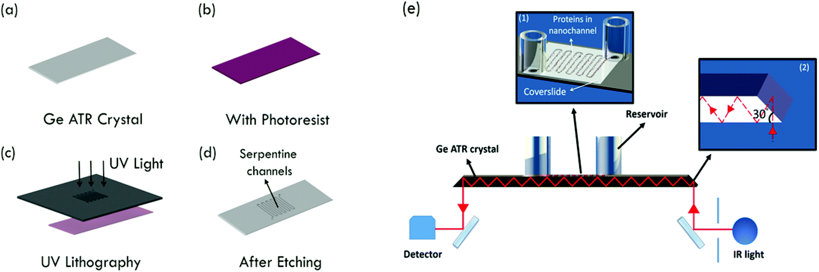 | ||
| Fig. 1 (a)–(d) Fabrication scheme of serpentine nanochannels on Ge ATR crystals. (e) Schematic set up for ATR-IR spectroscopy on a Ge nanochannel device. Inset (1) shows an enlarged image of the nanochannel region. Inset (2) shows chip edges ground to 30° angle to facilitate 60° angle of incidence. | ||
Experimental section
Device fabrication
Ge nanofluidic devices used in our experiments were fabricated using conventional semiconductor device fabrication techniques in a class 1000 cleanroom facility. The device design consists of serpentine channels of 600 μm width and 10 nm depth with uniformly spaced post arrays. Each post is 100 μm long and 30 μm wide. Spacing between adjacent posts is 30 μm. Posts were designed with round edges to help minimize pinning of liquid, thereby reducing the chances of bubble formation.12 Post arrays help to fill the channels by a leading edge capillary flow and to maintain the aspect ratio for effective sealing of serpentine channels using polymer assisted room temperature bonding (Fig. 1).First, ATR-IR optical elements were obtained by dicing 0.5 mm thick 4-inch Ge (100) wafers (University Wafer, Boston) to a size of 52(L) × 20(W) mm2. Diced substrates were polished to an angle of 30° along the short edges on both sides of the Ge substrates, to facilitate 60° angle of incidence. After polishing, substrates were immersed in 2% Extran neutral solution (VWR, Germany) for 1 h, followed by iso-propanol immersion for 1 h to remove all impurities from polishing, rinsed thoroughly with ultrapure deionized water and blow dried with N2. Before the fabrication process, substrates were further cleaned using acetone and iso-propanol by ultra-sonication for 2 minutes, rinsed using ultrapure deionized water and dried with N2 to ensure a clean surface. A photoresist (S1813, Shipley Inc.) was spin-coated on Ge substrates at 4000 rpm for 25 s and baked at 90 °C for 1.5 min. Fluidic channel patterns were transferred from a chromium photomask to the photoresist using a one-step photolithography (EVG620 mask aligner) process. After UV exposure (8.5 s at 10 mW cm−2), the photoresist was developed using MF 319 (Shipley Inc.) for 35 s. Photoresist patterns were transferred to a Ge substrate using reactive ion etching (RIE Plasmalab 80+, Oxford Instruments). An initial de-scum process using 100 sccm O2, 300 mTorr pressure and 150 W RF power for 2 min to remove any residual photoresist in the region of interest was followed by etching using 10 sccm CHF3, 3 mTorr pressure and 100 W power for 1 min. Surface profiler measurements (Alpha step IQ, KLA Tencor) and atomic force microscopy (AFM Nanoscope III, Veeco) measurements confirmed that the depths were around 10 nm with the average surface roughness in etched and un-etched regions less than 0.5 nm (Fig. 2).
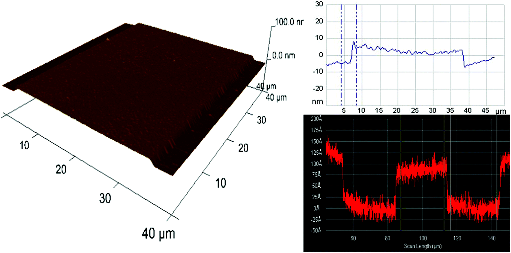 | ||
| Fig. 2 AFM 3D profile showing a section of one of the post regions in the 10 nm deep nanochannel. Top right is the height measurement obtained using AFM and the bottom right image is from surface profiler measurements, showing the height of the nanochannels of ∼10 nm. | ||
Through holes (1 mm diameter) were drilled using a sand-blaster on glass coverslides (no. 1, gold seal, 25 × 25 mm) to form the inlet/outlet of the loading reservoirs. Then the coverslides were cleaned with a piranha solution (98% H2SO4 and 30% H2O2 in 1![[thin space (1/6-em)]](https://www.rsc.org/images/entities/char_2009.gif) :1 ratio) for 15 min, rinsed thoroughly in deionized water and dried in a N2 stream. Cleaned glass coverslides were then dehydration baked at 200 °C for 3 min before spin-coating PSQ on the coverslide at 3000 rpm for 30 s. PSQ was freshly prepared before coating by mixing 2 parts of xylene and 1 part of Hardsil (AP grade, Gelest Inc.) and filtered using a 0.45 μm PTFE membrane (Basic Life Inc.). Coverslides with spun-on PSQ were then baked at 240 °C for 30 min.
:1 ratio) for 15 min, rinsed thoroughly in deionized water and dried in a N2 stream. Cleaned glass coverslides were then dehydration baked at 200 °C for 3 min before spin-coating PSQ on the coverslide at 3000 rpm for 30 s. PSQ was freshly prepared before coating by mixing 2 parts of xylene and 1 part of Hardsil (AP grade, Gelest Inc.) and filtered using a 0.45 μm PTFE membrane (Basic Life Inc.). Coverslides with spun-on PSQ were then baked at 240 °C for 30 min.
Hydrogen peroxide (H2O2) etches Ge vigorously and thus cannot be used to clean the substrates.24,25 Alternatively, UV-ozone cleaning was used for 15 min to render the Ge surface clean and hydrophilic, important for good bonding and effective filling of channels. Cleaned Ge substrates and PSQ coated coverslides were exposed to O2 plasma (17 sccm O2, 50 W RF power, 0.18 mbar, 1 min) in a RIE chamber. The plasma treated PSQ surface was brought into contact and aligned to overlap loading holes with fluidic patterns on the Ge substrate, then pressed gently with tweezers to enable effective bonding. Silanol (Si–OH) groups on PSQ react with germanol (Ge–OH) groups on the Ge substrates, forming Si–O–Ge bonds through a condensation reaction.26 The presence of an –OH surface termination on Ge was previously confirmed by angle resolved X-ray photoelectron spectroscopy (ARXPS).27 Finally, silica reservoirs were bonded over the loading-hole regions using a UV-curable glue (no. 108, Norland optical adhesives). With this step, fabrication was complete and devices were ready for experiments (Fig. 3a).
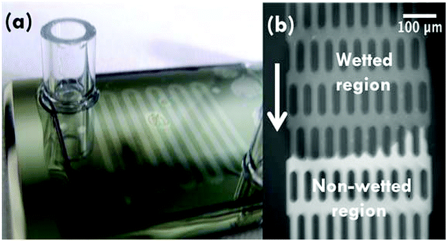 | ||
| Fig. 3 (a) PSQ-bonded serpentine nanochannel device. (b) Optical micrograph showing the filling of channels by means of capillary flow. White arrow indicates the flow direction. | ||
Measurement of ATR-IR spectra of HSA
To prove the function of the manufactured devices, human serum albumin (HSA) was chosen, as it is a well-studied globular protein abundantly present in blood with concentrations around 50 g L−1.26 Purified HSA (Sigma-Aldrich) was used as supplied, without further purification. All experiments were conducted in D2O (VWR) as the solvent. 60 mg HSA powder was dissolved in 200 μL D2O and used immediately for experiments. Nanochannels were loaded with 20 μL of stock solution in the reservoirs and devices were stored in an airtight container until the onset of experiments, to minimize the exchange of D2O with atmospheric water vapour.ATR-IR spectra of HSA protein in D2O were recorded with a FTS 3000 Fourier Transform IR spectrometer (Bio-Rad, Palo Alto, CA) using a liquid N2 cooled mercury cadmium telluride (MCT) detector. The spectrometer was purged with N2 before and during experiments in order to minimize the content of atmospheric water vapour. For multiple reflection ATR-IR measurements, a horizontal ATR mirror unit (Spectra Tech 0001-100, Stamford, CT) was used. The built-in crystal plate of the ATR mirror unit was replaced by a PTFE plate, on which the Ge substrate with nanochannels was placed during IR measurements. Details on the experimental setup have been described before.4,5 250 scans were co-added for each IR spectrum with a spectral resolution of 4 cm−1. IR spectra were recorded in both s- and p-polarizations. In this work, each IR spectrum is displayed as absorbance, defined as A = −log10(Isam/Iref), where Isam and Iref are the IR light intensity of sample and background measurements, respectively, with the latter carried out at the Ge–air interface before nanochannels were filled with any solution. For comparison, the spectra of D2O were recorded by placing a drop (20 μL) of D2O on a plain Ge IRE without nanochannels.
Advantages of PSQ bonding
Polymer-assisted bonding as used here has the advantage that it requires no heating step. For example, polydimethylsiloxane (PDMS) is a commonly used bonding material, but has a low Young's modulus (360–870 kPa) and thus limited to channels above 100s of nanometers in depth. Here we use PSQ, with a very high Young's modulus (∼800 MPa),22 to effectively bond 10 nm deep nanofluidic channels from a modified procedure suitable for Ge IREs. Anodic bonding of Si substrates using glass coverslides has been previously reported to obtain microfluidic devices for IR spectroscopy,7,8 by which two materials with different melting temperatures can be bonded at moderate temperatures (200–500 °C). Ge–glass bonding has also been reported at moderate temperatures, showing typical bond strengths around 10 MPa,28 higher than the fracture strength of glass. So, fluidic devices with permanent bonding make reusability impossible. This may not be a problem when inexpensive Si substrates are used, but becomes a limitation when expensive materials like Ge are involved. Another advantage of PSQ bonding is that it can be de-bonded and the Ge substrates can be reused again. Bonded substrates were soaked in diluted (1/10) buffered hydrogen fluoride (BHF, 6:1 volume ratio of 40% NH4F in H2O and 49% HF in H2O) for 15–30 min to separate the PSQ spun coverslides from the substrate easily. De-bonded substrates were later rinsed thoroughly with deionized water and dried in a N2 stream. Cleaned substrates can be re-bonded using the same procedure mentioned above. Rebonding can be done several times without affecting the quality of bonding.
Results and discussion
First measurements were conducted with 300 g L−1 (4.5 mM) HSA in D2O. A separate experiment with D2O alone was performed for reference. Absorbance spectra of D2O alone and HSA in D2O are shown in Fig. 4. The amide I band of proteins is predominant between 1600–1700 cm−1,29 indicating the presence of protein in the nanochannels. The observed absorbance maxima at 1649 cm−1 correspond to the amide I vibrations in an α-helix conformation.29 The observation is in agreement with the dominance of α-helical segments in crystalline HSA (PDB ID: 1AO6), confirming the absence of protein aggregation in our device. The measured data for HSA protein in D2O show that there is a shift in the bands to lower wavenumbers when compared to the amide I and II frequencies of HSA in H2O reported in the literature.30 For example, α-helix bands for the amide I region are observed at 1649 cm−1 in our experiments, compared to the reported value of 1656 ± 2 cm−1 for HSA in H2O.30 A shift between 3–10 cm−1 towards the lower wavenumber has been typical of different proteins when D2O is used as the solvent instead of H2O, due to the small NH contribution to the amide I mode and the associated isotope effect.26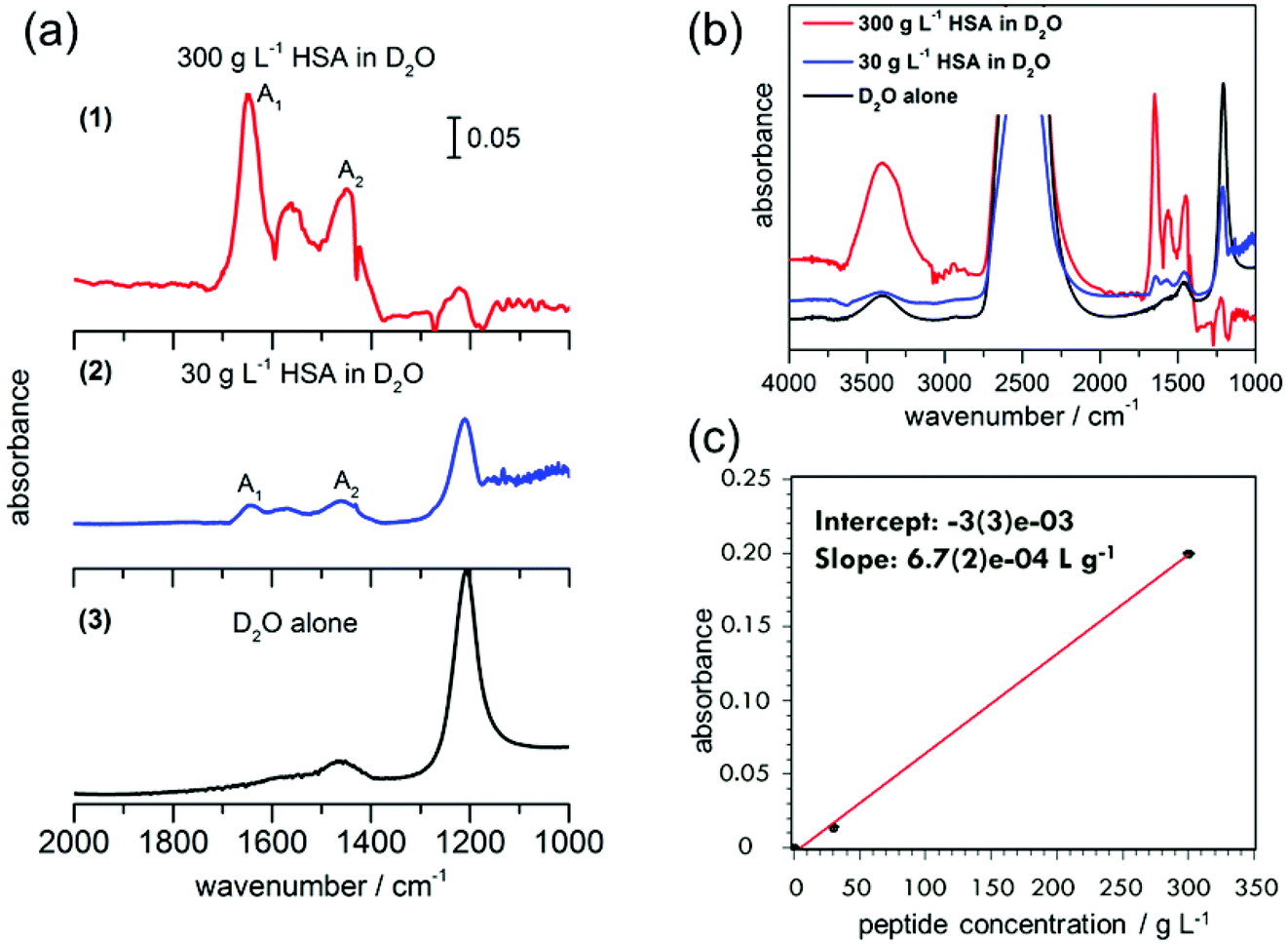 | ||
| Fig. 4 (a) ATR-IR spectra of (1) HSA in D2O (300 g L−1), (2) HSA in D2O (30 g L−1) in 10 nm deep Ge ATR-IR nanochannel devices and (3) bulk D2O alone obtained on the Ge ATR-IR crystal. A1 (1649 cm−1) and A2 (1450 cm−1) indicate the amide I and amide II peaks, respectively. (b) The extended spectra of the same, from 4000 to 1000 cm−1. (c) Peak absorbance of amide I mode versus concentration. | ||
Absorptions between 1500–1600 cm−1 correspond to the amide II bands of the proteins and peptides in H2O.29 Upon deuteration, the amide II mode shifts from ∼1550 cm−1 to 1450–1490 cm−1.29 In the ATR-IR spectrum of HSA in D2O, bands are visible both at 1450 cm−1 and 1560 cm−1. The peak centred around 1560 cm−1 that contains at least three main contributions at 1538 cm−1, 1552 cm−1 and 1571 cm−1 closely resembles the amide II mode of a polypeptide chain with incomplete H/D exchange. The weak association mode of D2O, which is centred around 1555 cm−1,31 contributes only in negligible amounts to the observed absorption, as is shown by the small contribution (compared to the O–D stretching mode) in the D2O spectrum. Amino acid side chains, which may contribute to the spectrum in this region, are aspartic acid and glutamic acid, with their respective COO− stretching modes at 1584 cm−1 and 1565 cm−1.29 HSA contains 6.7% aspartic acid and 10.3% glutamic acid,29 likely to have some contribution to the peaks at ∼1560 cm−1. The other possible contribution to this peak is from the incomplete H/D exchange in the protein.
In order to test the sensitivity of our device, we performed a second experiment with one order of magnitude lower HSA concentration in D2O, 30 g L−1 (0.45 mM). Although the absorbance peaks are not as prominent as in the 300 g L−1 experiment, the amide I and II peaks can still be clearly distinguished. A small peak is also observed in the D2O spectrum without HSA around 1450 cm−1, which is assigned to the H–O–D bending vibration. Hence the absorption at 1450 cm−1 can be assigned to a superposition of the H–O–D bending mode with the amide II mode of HSA in D2O.17,18 In comparison with the amide I peak height, the amide II peak is not so prominent for 30 g L−1, but it is clear from the experiment with higher HSA concentration that the peak at 1450 cm−1 is indeed a mixture of H–O–D and amide II components.
The presence of an amide II mode of the H-form of a protein in D2O solution may stem from two different causes. If the peptide chain contains hydrophobic portions that are inaccessible to water, residual H remains on the chains. For HSA, however, 1 h after sample preparation, almost complete H exchange was reported previously.26 In contrast, kinetic exchange experiments at 25 °C show still a considerable fraction of H-form amide II after >4 h of HSA exposure to D2O. In the spectra observed here for 300 g L−1 and 30 g L−1 HSA in D2O too, residual OH stretching modes are observed around 3400 cm−1, indicating that indeed H is still present as a minor (20% fraction for 300 g L−1 and 3% for 30 g L−1 from estimating peak areas), but detectable, fraction. In the total system, there are about 5% H compared to D (one order smaller for the 30 g L−1 case), so residual contributions of OH or non-exchanged amide are to be expected. The small bulge observed at 1644 cm−1 can be assigned to amide I vibrations in random coil conformation, but in the case of the incomplete H–D exchange, the 1644 cm−1 peak could most likely be from H–O–H bending. In both D2O and HSA in D2O solutions, 2 more bands are observed. The band at 2488 cm−1 is assigned to the O–D stretching mode of the D2O solvent and the one at 1224 cm−1 to a D–O–D bending mode.29 Hence our results indicate the presence of globular HSA proteins under partially deuterated conditions.
The peak absorbance of the amide I mode increases linearly with the protein concentration. Because the peak positions of deuterated and non-deuterated forms are similar, the area in the amide I mode can still be used for concentration determination. The slope of the line of best fit provides the sensitivity of our device as 6.7 × 10⁻⁴ g L−1, i.e. 0.1 mM (6.1 × 10¹⁵ molecules per L, Fig. 4c). Furthermore, the limit of detection of our device could be obtained from the plot, by analyzing the signal corresponding to three times the signal of the blank measurement. With an intercept error of 3 × 10⁻³, this will be an absorbance of 9 × 10⁻³, which corresponds to a concentration of 13.4 g L−1 (corresponding to 7.9 × 10¹⁰ molecules in the device, with a HSA molecular weight of 66478 g mol−1). This corresponds to a detection limit of 0.2 mM.
Conclusions
In conclusion, we presented a simple scheme to fabricate sub-nanoliter volume nanofluidic devices on Ge ATR crystals and demonstrated its potential applications for protein analysis by FT-IR using HSA. A nanochannel of 10 nm depth offers the advantage of a very high surface-to-volume ratio (2 × 10⁶), two orders of magnitude higher than a 1 μm deep channel of the same length and width, thus confining all molecules close to the IRE surface for effective near-field IR absorption, thereby minimizing sample volume consumption. Our results show IR peaks for the amide I and amide II regions of HSA, in agreement with earlier published results. ATR-IR spectra show the characteristic amide I vibrational modes proving the possibility to obtain the IR absorption spectra of samples with 650 pL volume comprising ∼1.7 × 10¹¹ molecules (0.45 mM), with a detection limit even below that. This detection limit can, in principle, be further reduced by appropriate background measurement strategies. Previous studies show that difference absorbance down to 10−4 can be routinely detected.5 This absorbance corresponds to 2 × 10⁹ molecules in the device, i.e. 5 μM. This value is at par with the best results achieved through preconcentration of analytes before IR measurements, but our method eliminates the need for such tedious procedures.3 The dominance of the absorption typical of helical segments in the amide I mode shows the absence of protein aggregation. The advantages of this device include its reusability and the need for extremely small sample volume (sub-nanoliters), making it useful for studying a wide range of samples. Furthermore, this device may enable FTIR analysis of low copy number proteins. In addition to proteins, this device can also be used for ATR-IR spectroscopy of DNA, DNA–protein complexes and chemical analytes, exploiting the high specificity of IR spectroscopy.7,8,32Acknowledgements
The authors acknowledge technical assistance from AS Nano Core Facilities. This work was supported by the AS Nano Science and Technology Program, AS Integrated Thematic Project (AS-103-TP-A01), the Ministry of Science and Technology (MOST), Taiwan (102-2112-M-001-005-MY3, 103-2923-M-001-007-MY3, 104-2119-M-001-011), and the Asian Office for Aerospace Research and Development (#FA2386-12-1-4002). S. N. thanks the International Max Planck Research School for Surface and Interface Engineering in Advanced Materials (IMPRS-SurMat) for a PhD scholarship. This work furthermore benefited from support through the MOST/DAAD (Deutscher Akademischer Austauschdienst) Project Based Personnel Exchange Program (#100-2911-I-001-508 and #50754480).Notes and references
- P. Abgrall and N. T. Nguyen, Anal. Chem., 2008, 80, 2326–2341 CrossRef CAS PubMed.
- D. C. Harris and M. D. Bertolucci, Symmetry and Spectroscopy: An Introduction to Vibrational and Electronic Spectroscopy, Dover Publications Inc., New York, 1989 Search PubMed.
- A. Gonzalvez, S. Garrigues, M. de la Guardia and S. Armenta, Anal. Methods, 2011, 3, 43–52 RSC.
- M. Milosevic, Appl. Spectrosc., 2013, 67, 126–131 CrossRef CAS PubMed.
- S. Nayak, P. U. Biedermann, M. Stratmann and A. Erbe, Phys. Chem. Chem. Phys., 2013, 15, 5771–5781 RSC.
- S. Nayak, P. U. Biedermann, M. Stratmann and A. Erbe, Electrochim. Acta, 2013, 106, 472–482 CrossRef CAS.
- E. Karabudak, B. L. Mojet, S. Schlautmann, G. Mul and H. J. Gardeniers, Anal. Chem., 2012, 84, 3132–3137 CrossRef CAS PubMed.
- R. Herzig-Marx and K. T. Queeney, Anal. Chem., 2004, 76, 6476–6483 CrossRef CAS PubMed.
- K. L. Chan, S. Gulati, J. B. Edel, A. J. de Mello and S. G. Kazarian, Lab Chip, 2009, 9, 2909–2913 RSC.
- Z. Wang, D. Voicu, L. Tang, W. Li and E. Kumacheva, Lab Chip, 2015, 15, 2110–2116 RSC.
- P. Wagli, Y. C. Chang, K. Hans, A. Homsy, L. Hvozdara, H. P. Herzig, M. Sigrist and N. F. de Rooij, Anal. Chem., 2013, 85, 7558–7565 CrossRef CAS PubMed.
- A. V. Ewing, G. S. Clarke and S. G. Kazarian, Biomicrofluidics, 2016, 10, 024125 CrossRef PubMed.
- Y. J. Oh, T. C. Gamble, D. Leonhardt, C. H. Chung, S. R. Brueck, C. F. Ivory, G. P. Lopez, D. N. Petsev and S. M. Han, Lab Chip, 2008, 8, 251–258 RSC.
- D. Bottenus, Y. J. Oh, S. M. Han and C. F. Ivory, Lab Chip, 2009, 9, 219–231 RSC.
- http://www.crystran.co.uk/optical-materials/silicon-si .
- E. Karabudak, Electrophoresis, 2014, 35, 236–244 CrossRef CAS PubMed.
- S. E. Glassford, B. Byrne and S. G. Kazarian, Biochim. Biophys. Acta, 2013, 1834, 2849–2858 CrossRef CAS PubMed.
- M. Voue, E. Goormaghtigh, F. Homble, J. Marchand-Brynaert, J. Conti, S. Devouge and J. D. Coninck, Langmuir, 2007, 23, 949–955 CrossRef CAS PubMed.
- S. Devouge, J. Conti, A. Goldsztein, E. Gosselin, A. Brans, M. Voue, J. De Coninck, F. Homble, E. Goormaghtigh and J. Marchand-Brynaert, J. Colloid Interface Sci., 2009, 332, 408–415 CrossRef CAS PubMed.
- J. Schartner, J. Guldenhaupt, B. Mei, M. Rogner, M. Muhler, K. Gerwert and C. Kotting, J. Am. Chem. Soc., 2013, 135, 4079–4087 CrossRef CAS PubMed.
- M. Liley, T. A. Keller, C. Duschl and H. Vogel, Langmuir, 1997, 13, 4190–4192 CrossRef CAS.
- J. Gu, R. Gupta, C. F. Chou, Q. H. Wei and F. Zenhausern, Lab Chip, 2007, 7, 1198–1201 RSC.
- T. Leichlé, Y. L. Lin, P.-C. Chiang, S. M. Hu, K. T. Liao and C. F. Chou, Sens. Actuators, B, 2012, 161, 805–810 CrossRef.
- N. Cerniglia and P. Wang, J. Electrochem. Soc., 1962, 109 Search PubMed.
- W. Primak, R. Kampwirth and Y. Dayal, J. Electrochem. Soc., 1967, 114, 88–91 CrossRef CAS.
- S. A. Sukhishvili and S. Granick, J. Chem. Phys., 1999, 110, 10153–10161 CrossRef CAS.
- K. Y. Byun, I. Ferain, P. Fleming, M. Morris, M. Goorsky and C. Colinge, Appl. Phys. Lett., 2010, 96, 102110 CrossRef.
- M. M. R. Howlader, M. G. Kibria and F. Zhang, Mater. Lett., 2010, 64, 1532–1535 CrossRef CAS.
- E. Goormaghtigh, V. Cabiaux and J.-M. Ruysschaert, in Subcellular Biochemistry, ed. H. J. Hilderson and G. B. Ralston, Plenum Press, New York, 1994, vol. 23 Search PubMed.
- J. Kong and S. Yu, Acta Biochim. Biophys. Sin., 2007, 39, 549–559 CrossRef CAS PubMed.
- L. K. Tamm and S. A. Tatulian, Q. Rev. Biophys., 1997, 30, 365–429 CrossRef CAS PubMed.
- T. Maiyoshi, R. Yamaguchi, K. Ishibashi, K. Miyamoto, Y. Kimura and M. Niwano, presented in part at the MEMS IEEE 20th International Conference on IEEE, Kobe, Japan, 2007.
Footnotes |
| † Joint first authors. |
| ‡ Present address: Department of Chemistry, University of Oxford, South Parks Road, Oxford, OX1 3QR, UK. |
| This journal is © The Royal Society of Chemistry 2017 |