DOI:
10.1039/C6RA03449G
(Paper)
RSC Adv., 2016,
6, 46372-46379
Organic–inorganic hybrid cathodes: facile synthesis of polypyrrole/zinc oxide nanofibers for low turn-on electron field emitters
Received
5th February 2016
, Accepted 1st May 2016
First published on 3rd May 2016
Abstract
The identification of new materials capable of sustaining a high electron emission current is a key requirement in the development of the next generation of cold cathode devices and technology. Compatibility with large volume material production methods is a further important practical consideration with solution chemistry-based methods providing for routes to industrial scale-up. Here we demonstrate a new class of organic–inorganic hybrid material based on polypyrrole and zinc oxide (PPy/ZnO) nanofibers for use as a low-cost large-area cathode material. Solution chemistry based surfactant chemical oxidation polymerisation is used to synthesise the nanofibers and the macroscopic turn-on electric field for emission has been measured to be as low as 1.8 V μm−1, with an emission current density of 1 mA cm−2 possible for an applied electric field of less than 4 V μm−1. Specific surface area measurements reveal a linear increase in the nanofiber surface area with ZnO incorporation, which when coupled with electron microscopy and X-ray diffraction analysis reveals that the wurtzite ZnO nanoparticles (around 45 nm in size) act as nucleation sites for the growth of PPy nanofibers. Our study demonstrates for the first time how an inorganic nanocrystal acting as a nucleation site allows the tailored growth of the organic component without diminishing the overall electrical properties and opens the potential for a new type of organic–inorganic hybrid large-area cathode material. The broader impacts and advantages of using hybrid materials, when compared to other composite nanomaterial systems, as large area cathode materials are also discussed.
1. Introduction
Electron field emission refers to the emission of electrons from the surface of a material under the influence of an applied electric field via quantum tunneling.1,2 The magnitude of the emission current is principally determined by the electric field found at the emitter surface, referred to as the local electric field, and the magnitude of the work function, represents the potential barrier for emission.2,3 In this way field emission offers some significant advantages over photoemission and thermionic emission processes in terms of more rapid device turn-on time, smaller device dimensions accompanied by less expensive packaging, low energy consumption with high efficiency, and coupled with room temperature operation negating the need for direct heating; all leading to so-called cold cathode technology.1–3 These characteristics have led to a wide range of applications in vacuum micro- and nanoelectronics including electron sources for rf and microwave electronics,4 high electron brightness sources accompanied by a narrow energy spread of the emitted electrons for lithography,5 electron holography,6 large area field emission displays7 and solid state lighting.8
The field emission (FE) current arises from quantum tunnelling of electrons under the influence of an electric field from filled electron states at, and just below, the material's Fermi energy (chemical potential). For any cathode material the magnitude of this emission electron current density is governed by which of the following three transport processes3 is the emission rate limiting step: (1) the concentration and availability of free electrons in the emitter or the injection of electrons into the emitter from another source, usually a metallic or heavily doped Si substrate (the so-called injection controlled emission process), (2) the transport of electrons to the emitter front surface (transport controlled emission), or (3) the emission of electrons via Fowler–Nordheim quantum tunnelling through an approximately triangular surface potential barrier (front surface controlled emission). This final process strongly depends upon the emission area and geometry (roughness) of the emitter, which has a strong influence on the magnitude of the electric field in the vicinity of the emission site. A knowledge of which of these three processes is the rate determining step for emission is therefore a crucial feature in the design, synthesis and evaluation new materials for cathode applications. Materials with high geometry aspect ratios and/or rough surfaces will experience large (local) electric fields (typically several V nm−1) in the vicinity of the surface as the field lines concentrate here. This amplification of the applied field is characterized by the dimensionless field enhancement factor, β. It is the magnitude of the local electric field, in conjunction with the work function, which determines the magnitude of the emission current arising from electron tunnelling through the emitter – vacuum potential barrier.9
Many functional materials have been studied as potential cathodes including single- and multiwalled carbon nanotubes (CNTs),10 carbon nanotube–polymer composites,11 diamond films,12 silicon nanowires,13 ultrananocrystalline diamond (UNCD),14 and a variety of wide electronic band gap metal oxide semiconductors (ZnO, SnO2, TiO2).15–17 Diamond thin films have been extensively investigated as cathode materials due to their low, and sometimes negative, electron affinity (potential barrier to emission) but their overall FE and transport properties are inferior when compared to other materials due to the largely empty conduction band at room temperature arising from its wide electronic band gap. UNCD films consist of wide band gap sp3 grains and low band gap sp2 graphitic grain-boundaries. Electron emission is determined by the transport of electrons from the sp2 region to the low affinity barrier in the sp3 region. Carbon nanotubes are another promising cathode material due to their excellent mechanical properties, intrinsic high electrical conductivity and their one-dimensional high aspect ratio provides the high local field necessary for emission. However, their typical growth temperatures are high (typically >700 °C) and the degradation of CNTs by oxidation and heating effects at the interface between the nanotubes and the conducting substrate,18 has limited to date their practical applicability in FE devices. Therefore, other functional materials with high aspect ratios and/or rough surfaces with good transport properties and which can be readily synthesized are being actively researched.
One such material system capable of large volume production is based on conducting polymers, where such materials have already demonstrated applications in solar cells,19 as gas sensors,20 and in batteries.21 However, the field emission properties of these materials, especially as part of a hybrid or composite material, have not been previously explored and are the subject of this study. Polypyrrole (PPy) is considered to be one of the most stable conducting polymers having a work function around 5.1 eV, comparable to that found in CNTs (typically 4.6–5.0 eV), and which can be easily produced in different morphological forms including nanotubes and nanorods,20 and as nanofibers.22 As discussed above being able to produce materials with a high aspect ratio is an important consideration for cathode materials as such materials tend to lead to high field enhancement factors and low turn-on electric fields. Hence there is considerable interest in carbon based materials that can be readily synthesized over large areas; PPy nanofibers is one such material. In addition to ready ease of production it is also possible to combine PPy with other materials, such as metal oxides, to form hybrid materials. Such hybrid nanomaterials have some distinct advantages in which different large volume production techniques, such as solution processing11 or screening printing,23 can be employed, and which allows for accurate control of the constituents thereby tailoring the material properties to the overall required specifications without significant material wastage. A hybrid nanomaterial also allows for selective additional functionality not found with any of the individual components on their own. Therefore, in the present study we have synthesized, using solution-based surfactant-controlled chemistry, one-dimensional nanofibers of PPy and hybrid PPy/ZnO using cubic-shaped wurtzite ZnO nanoparticles. ZnO was selected as the inorganic component as it is a relatively available metal oxide whose synthesis is compatible with solution chemistry methods and has a work function similar to that of PPy. ZnO in various forms has been studied as a potential cathode itself with a current density of 2 mA cm−2 at a (high) turn-on applied field of 7 V μm−1 measured from nanoneedle arrays using selenium-controlled vapor phase deposition.24 Controlling the ZnO nanorod density is also possible by varying the amount of Zn vapour supersaturation during vapour phase transport growth with a high level of initial Zn supersaturation favoring lower densities of emitters; comparable turn-on electric fields of 7 V μm−1 have also been measured.25 In this study ZnO is being used as cubic-shaped nanoparticles to increase the PPy surface area rather than in nanorod form to produce superior emission characteristics (i.e. low turn-on fields). In this study we report the synthesis, structural and electronic properties of organic–metal oxide hybrid nanomaterials with the aim of assessing their potential as a cold cathode material. Our specific aims are to relate the morphology and specific surface area of the material produced to the constituent parts and explore the field emission properties of the resulting hybrid material. More generally we wish to understand the factors that are important in the design of organic–inorganic hybrid cathode materials which can be extended to other hybrid material systems.
2. Synthesis and experimental details
2.1 Synthesis of ZnO nanoparticles
Wurtzite ZnO cubic-shaped nanoparticles were synthesized using a hydrothermal process. A salt solution of Zn(NO3)2·6H2O (50 mM) was prepared in 100 ml doubled distilled water and refluxed at 90 °C for two hours followed by the addition of 50 mM cetyltrimethylammonium bromide (CTAB) as a capping agent and 1 M ammonia to increase the pH of the solution. Thereafter, a separately prepared solution of 50 mM NaOH was added drop-wise and the reaction was allowed to continue for two hours at the same temperature. After this time the solution was allowed to naturally cool down to room temperature and the ZnO nanoparticles were separated out, washed and then dried at 60 °C overnight. The synthesis of ZnO nanoparticles in aqueous medium follows the reaction scheme| | |
NH3 + H2O → NH4+ + OH−
| (1) |
| | |
Zn2+ + 4OH− → Zn(OH)42−
| (2) |
| | |
Zn2+ + 4NH3 → Zn(NH3)42+
| (3) |
| | |
Zn(OH)42− → ZnO + H2O + 2OH−
| (4) |
| | |
Zn(NH3)42+ + 2OH− → ZnO + 4NH3 + H2O
| (5) |
2.2 Synthesis of PPy/ZnO hybrid nanofibers
Polypyrrole/ZnO hybrid samples were prepared by surfactant assisted chemical oxidation with 5 and 10 wt% incorporation of ZnO and designated as samples P1 and P2, respectively. For the synthesis of sample P1, 20 mM solution of cationic surfactant CTAB was prepared in doubled distilled water containing 1 M HCl. 5 wt% of the above prepared ZnO nanoparticles was mixed with the surfactant solution by magnetic stirring for 45 min to ensure a homogeneous solution of ZnO nanoparticles. On the addition of separately prepared 45 mM oxidant solution of potassium persulfate white precipitates of (CTA)2S2O8 crystals were observed to be formed. As soon as the doubled distilled pyrrole monomer was added, black precipitates of PPy appeared; this was taken as an indication of the start of the polymerization process. The reaction was carried out for 12 hours to ensure completion of the polymerization process and finally terminated by the addition of a sufficient quantity of methanol. The prepared nano-powder was filtered and washed several times alternating between distilled water and methanol, and the resultant black powder was then dried. A similar method was used for the synthesis of the pure PPy sample without ZnO nanoparticle incorporation (sample P0) and with 10 wt% addition of ZnO (sample P2).
2.3 Sample structural characterization
The surface morphology of the synthesized samples was investigated through scanning electron microscopy (SEM) studies carried out using a LEO 440 Electron Microscope. The ZnO nanoparticles were analyzed by high resolution transmission electron microscopy (TEM) carried out at FEI using a Tecnai G2 F30-STWIN instrument. The crystallinity of the as-prepared ZnO nanoparticles and the PPy/ZnO samples was also investigated by X-ray diffraction studies performed using a Philips X'Pert PRO PAN analytical X-ray diffractometer employing Cu-Kα radiation. The samples were further investigated by Fourier transform infrared (FTIR) spectroscopy using a Nicolet 5700 spectrophotometer. Each sample's specific surface area was determined via Brunauer–Emmett–Teller (BET) measurements of nitrogen isotherms carried out at 77 K using a Gemini 2380 BET instrument.
2.4 Field emission characterization
Two terminal field emission measurements were carried out at room temperature in a high vacuum (better than 3 × 10⁻⁷ mbar) chamber created by a high efficiency turbomolecular pump backed with a rotary pump. The electron emission current was recorded by a Keithley 2410 source measure unit at different applied voltages in a sandwich (ITO/Teflon spacer/sample/silver) structure. ITO coated glass was used as an anode and a Teflon spacer (150 μm thickness) produced the vacuum gap. The turn-on field is defined as the applied electric field for an emission current density of 5 × 10⁻⁷ A cm−2. The applied field (anode voltage) was cycled up to a current density of about 1 mA cm−2 up to 15 times to gauge reproducibility and stability. Successive reduction in turn-on field with cycling of the field, sometimes referred to conditioning, is often seen in the cathode materials26 and often helps to clean the emitter surface.
3. Experimental results and discussion
3.1 Morphological properties of the samples
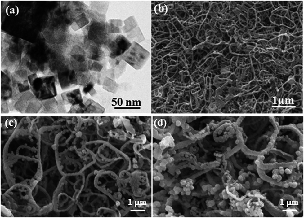
Shown in Fig. 1(a) is a high resolution transmission electron micrograph of the as-prepared ZnO nanoparticles and shows cubic-shaped nanostructures of 40–50 nm in dimension. In addition to the cubic-shaped ZnO nanoparticles some amorphous content can also be seen in the micrograph, which may be due to the traces of surfactant used for capping of the nanoparticles. Fig. 1(b) is a scanning electron microscope image of the PPy (only) nanofibers grown by surfactant-assisted chemical oxidation and shows the diameter to be about 100 nm with a typical length between 4 and 5 μm. Fig. 1(c and d) show the SEM micrographs of PPy/ZnO hybrid samples P1 and P2 having worm-like nanofibers of PPy/ZnO with a larger diameter of about 300 nm and a length about 5 μm; as a consequence the surface (emitting) area of samples P1 and P2 will be larger than sample P0. Note the presence of the nodule-like features in Fig. 1(c and d).
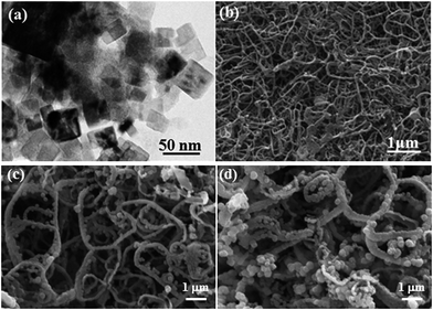 |
| | Fig. 1 (a) High resolution transmission electron microscope image of wurtzite ZnO nanoparticles showing that the nanoparticles are cubic in shape and are 40–50 nm in size. Scanning electron micrographs of (b) pure PPy, (c) PPy/ZnO sample P1, and (d) PPy/ZnO sample P2. | |
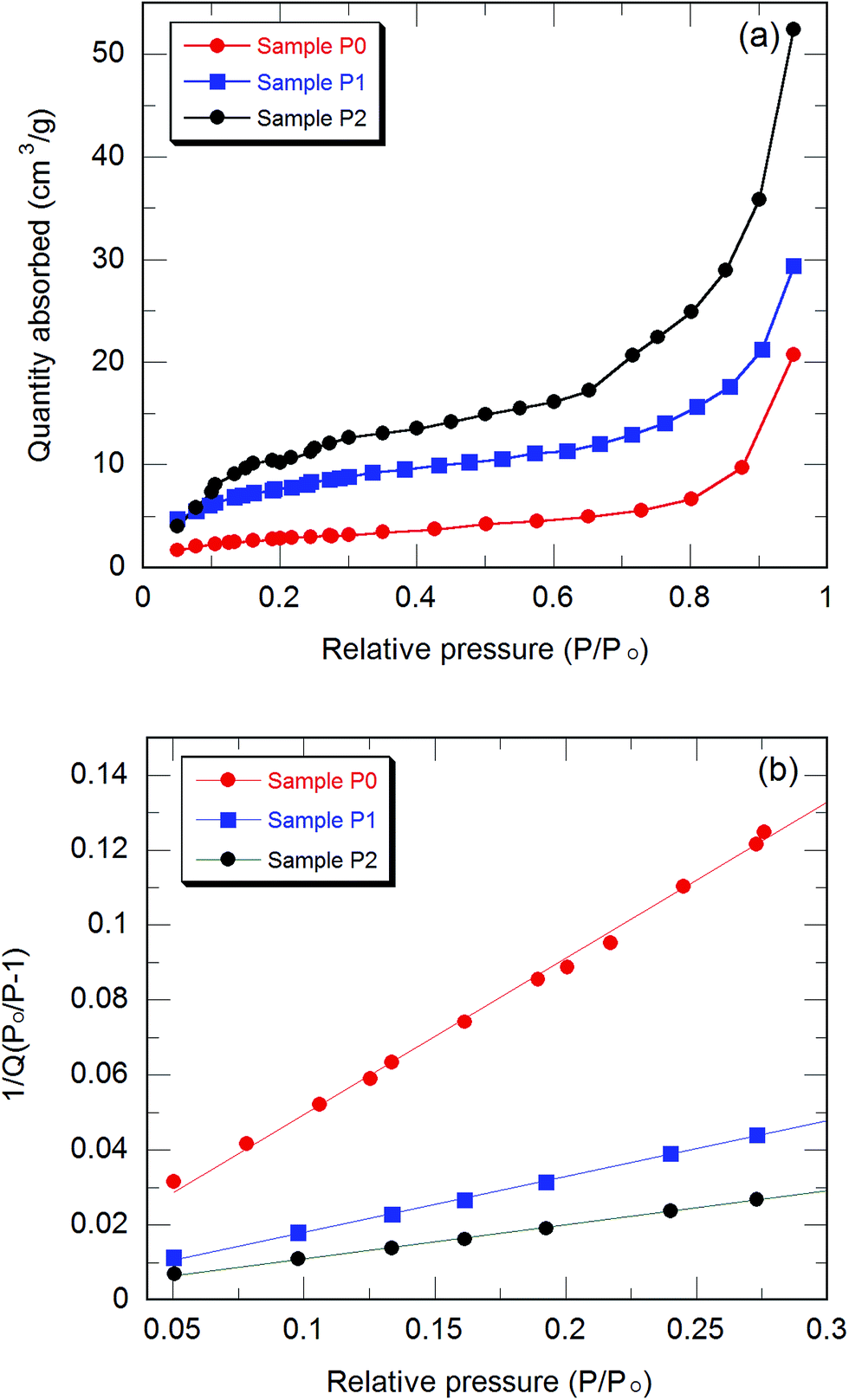
The specific surface area of the nanofibers was found from the analysis of the nitrogen adsorption isotherms (Fig. 2). Fig. 2(a) shows the isothermal curves between the quantity of gas molecules absorbed and relative pressure of nitrogen for the samples P0, P1, and P2. All the samples have S-shaped isothermal curves of type-II reflecting the mesoporous nature of the samples. The isotherm curves can be analysed into three regions: a concave shaped portion in the relative pressures range from 0.05 to 0.1, a linear portion up to relative pressure of 0.3 and a final section that is convex shaped portion above the relative pressure of 0.3. The linear portion from 0.05 to 0.3 of BET curve (Fig. 2(b)) characterizes the completion of first monolayer of adsorbed gas molecules and the start of the second adsorption layer and it is this region which can be used for the calculation of the specific surface area. Using standard BET analysis27,28 the BET specific surface areas for the samples P0, P1 and P2 are found to be 10.3, 28.4 and 48.2 m2 g−1.
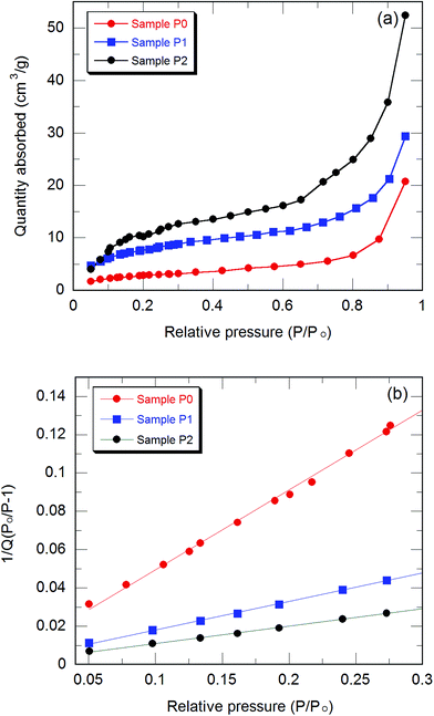 |
| | Fig. 2 (a) Isothermal curves between the absorption versus relative pressure (P/P0) for samples P0, P1, and P2. (b) Brunauer–Emmett–Teller specific surface area calculations samples P0, P1, and P2. Q is the volume of gas absorbed. | |
Addition of 5% ZnO results in an increase of the specific surface by 18.1 m2 g−1; doubling the ZnO content to 10% results in the surface area increasing by 37.9 m2 g−1, which is nearly double the increase with 5% ZnO inclusion. This strongly suggests that the addition of the ZnO is a controllable and scalable route to increase the specific surface area of the PPy nanofibers. We believe that the presence of the nodule-like features in the nanoribbons seen Fig. 1(c and d), and the linear increase in surface area with ZnO content from the BET measurements (Fig. 2) strongly suggest that the nanofibers are obtained via the nucleation of PPy surrounding the ZnO nanoparticles and are trapped in cages of surfactant micelles resulting in the formation of long PPy/ZnO nanostructures.
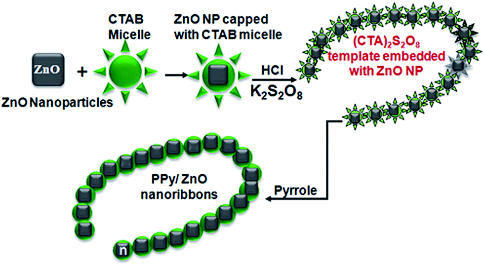
The detailed growth mechanism of the hybrid materials can be understood from surfactant assisted chemical oxidation, shown in Fig. 3. Surfactant molecules have hydrophilic heads and hydrophobic tails that form a monolayer at the water/air interface in aqueous solution. On increasing the concentration of the surfactant the critical micelle concentration (CMC) is reached at which the agglomeration of these molecules starts in the bulk of the solution, and above the CMC (0.89 mM for CTAB in water29) these surfactant molecules form spherical shaped micelles. The addition of ZnO nanoparticles to the micelle solution of CTAB, these nanoparticles are trapped into the cages of the micelles (Fig. 3). Addition of potassium persulfate solution promotes the self-assembly of the (CTA)2S2O8 crystals into nanofibers surrounding the ZnO nanoparticles. During the polymerization process the PPy chains are wrapped over these crystals into uniform layers of PPy which builds up to form chain-like nanostructures. The growth of pure PPy nanofibers (sample P0) follows a similar mechanism of formation but without ZnO presence and results in thinner structures being formed. Our results show that the presence of the ZnO enhances the surface area and roughness of the PPy nanofibers which, as shown later, is an important consideration in new cathode design.
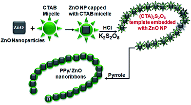 |
| | Fig. 3 Schematic representation of the formation of the PPy/ZnO nanofibers showing that an increase of surfactant above the critical micelle concentration spherical shaped CTAB micelles are formed, followed by trapping of the ZnO nanoparticles into the cages of the micelles. Subsequent addition of potassium persulfate solution allows for the self-assembly of the (CTA)2S2O8 crystals into nanofibers embedded with ZnO nanoparticles. Finally, the PPy chains are wrapped over these crystals during the polymerisation phase. | |
3.2 Structural and bonding properties of the samples
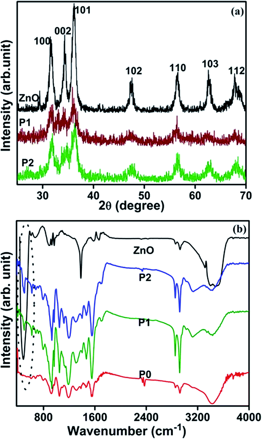
Fig. 4(a) shows the X-ray diffraction (XRD) pattern of the as-prepared ZnO nanoparticles and PPy/ZnO samples. It is observed that the XRD pattern of the ZnO nanoparticles comprises several peaks located at around 31.5, 34.3, 36.0, 47.4, 56.5, 62.7 and 67.8° associated with the reflections from the (hkl) planes (100), (002), (101), (102), (110), (103) and (112), respectively; these peaks being well matched with the wurtzite phase of ZnO.30 The observed X-ray peaks of ZnO are used to evaluate the crystallite size by Scherrer's method31 and the crystallite size is found to be around 40–45 nm in size; consistent with the electron microscopy results shown in Fig. 1(a), and which indicates that the ZnO phase consists of wurtzite nanocrystallites with a relatively narrow size distribution. The XRD pattern of the synthesized PPy/ZnO samples have peaks at similar diffraction angles as those observed from the pure ZnO nanoparticles but with reduced intensity, attributed to the presence of an amorphous PPy overlayer.
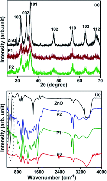 |
| | Fig. 4 (a) X-ray diffraction patterns of ZnO (black line) and PPy/ZnO samples P1 (red line) and P2 (green line) (b) FTIR spectra of ZnO nanoparticles (black line), the pure PPy sample P0 (red line) and the hybrid PPy/ZnO samples P1 (green line) and P2 (blue line). | |
The polymerization and formation of PPy/ZnO nanohybrids has also been confirmed by FTIR studies (Fig. 4(b)) performed on pure ZnO, PPy only (sample P0) and PPy/ZnO (samples P1 and P2). The FTIR spectrum of pure ZnO consists of an intense broad band around 488 cm−1, which is made up of two peaks centered at 437 and 505 cm−1, which are assigned to the Raman active E2 mode of hexagonal ZnO, and the band associated with defects which arises due to the oxygen vacancies in ZnO, respectively. The bands located around 1678, 3054 and 3476 cm−1 are attributed to the presence of O–H groups arising from the precursor materials and environmental exposure.32 The FTIR spectra of pure PPy and PPy/ZnO samples consist of all the fundamental bands of PPy located around 3422, 2854, 2922, 1558 and 1456 cm−1, associated with the N–H stretching vibration, C–H stretching vibration of methyl and methylene groups fundamental asymmetric (C![[double bond, length as m-dash]](https://www.rsc.org/images/entities/char_e001.gif) C) and symmetric (CN) ring stretching vibrations, respectively. The band observed at around 500 cm−1 in the FTIR spectrum of PPy/ZnO (encircled with dots) can be attributed to overlapping bands of PPy and ZnO. Besides these fundamental bands of PPy, further bands are seen in both PPy and PPy/ZnO samples at 1314, 1188, 1050, 924, and 796 cm−1, which are attributed to C–N stretching vibration, N–H in-plane deformation, C–H out-of-plane deformation, C–H in-plane deformation and C–H out-of-plane bending vibrations, respectively.32
C) and symmetric (CN) ring stretching vibrations, respectively. The band observed at around 500 cm−1 in the FTIR spectrum of PPy/ZnO (encircled with dots) can be attributed to overlapping bands of PPy and ZnO. Besides these fundamental bands of PPy, further bands are seen in both PPy and PPy/ZnO samples at 1314, 1188, 1050, 924, and 796 cm−1, which are attributed to C–N stretching vibration, N–H in-plane deformation, C–H out-of-plane deformation, C–H in-plane deformation and C–H out-of-plane bending vibrations, respectively.32
3.3 Field emission characterisation
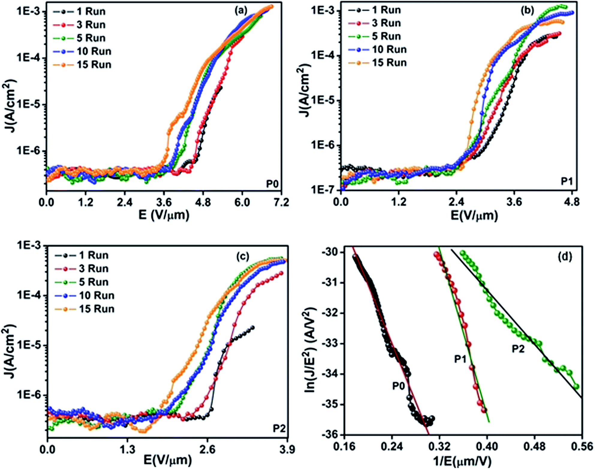
The field emission characteristics of the pure PPy and PPy/ZnO hybrid samples are shown in Fig. 5 and analyzed within the simplified Fowler–Nordheim (F–N) formulism relating the emission current density to the applied field via eqn (6) below 33| |
 | (6) |
where J is the current density, Φ is the work function of the emitter material, which for PPy is about 5.1 eV [ref. 34] and similar to that of ZnO nanoparticles (5.3 eV), E is the applied electric field and β is the field enhancement factor. The F–N constants a and b are 1.54 × 10⁻⁶ A V−2 eV and 6.83 × 10⁹ eV−3/2 V m−1, respectively. The field emission current density as a function of applied field is measured repeatedly, up to 15 cycles to gauge sample changes, on the PPy (sample P0) and PPy/ZnO samples P1 and P2. It is observed that with successive voltage (field) cycles the turn-on field decreases from 4.1 to 3.4 V μm−1 (after the 15th cycle of applied field) in PPy nanofibers (Fig. 5(a)) and from 2.6 to 1.8 V μm−1 in PPy/ZnO samples; the turn-on field for sample P1 is intermediate between sample P0 and P2, (Fig. 5(b and c)). The electron emission current is strongly dependent on the work function (Φ) and field enhancement factor (β). The value of β can be obtained from the so-called Fowler–Nordheim (F–N) plots of ln(J/E2) versus 1/E, Fig. 5(d), assuming the value of Φ is known. The straight lines found in the plot of ln(J/E2) vs. 1/E implies that the electrons are emitted via F–N tunnelling; an important result, as discussed later. The field enhancement factor (β) can then be determined from the slopes of the F–N plots via eqn (7)| |
 | (7) |
 |
| | Fig. 5 Field emission J–E characteristics of (a) pure PPy (sample P0), (b) PPy with 5 wt% incorporation of ZnO (sample P1), (c) PPy with 10 wt% incorporation of ZnO (sample P2). (d) Variation of ln(J/E2) versus 1/E characteristics of the samples P0, P1 and P2 in the usual Fowler–Nordheim representation. The straight lines indicate that the emission from these materials follows the Fowler–Nordheim emission mechanism. | |
Taking the work function of the PPy to be 5.1 eV, the value of β is calculated to be 1659, 1537 and 3846 for the samples P0, P1 and P2, respectively. The local electric field for sample P0 and P2 can be estimated from the product of the applied turn-on field multiplied by the field enhancement factor to be 5.6 and 6.9 V nm−1. The value of β is higher with sample P2 associated with the higher (rough) surface area and results in the highest local field and hence emission at the lower applied field.
4. Discussion of hybrid cathode design
The observation that the emission current can be satisfactorily fitted to the F–N type mechanism for the samples investigated is significant in a hybrid cathode material for three reasons. Firstly, it shows that the rate limiting step for emission is controlled by front surface tunnelling of the electrons into vacuum rather than transport of electrons through the PPy or injection from the back silver contact. This differs from reports of emission from other hybrid cathode systems such as multi-walled CNT–poly-(m-phenylenevinylene) (PmPV) polymer composites,35 where the emission characteristics are bulk transport limited. Here transport in the composite is percolation-controlled as a function nanotube mass fraction where threshold electric fields in the range of 8–14 V μm−1 were reported. For an ideal cathode the rate limiting step should be the final stage of transport i.e. F–N tunnelling through the potential barrier into the vacuum; this is what is observed in the case of the PPy/ZnO hybrid materials. Furthermore the data of Fig. 5(d) shows that the fit of the measured emission current density with electric field presented in F–N coordinates (1/E, ln(J/E2)) is excellent for the whole data range. This is important as it indicates that these PPy–ZnO hybrid cathodes are able to sustain current densities up to 1 mA cm−2 without saturation of the current. The maximum emission current density extracted from these samples is a few mA cm−2 in all the samples, however, the key result obtained here is that the current density occurs at successively lower applied electric fields. In the case of the CNT–PmPV cathode system, deviation from F–N behaviour was taken as a sign that the emission current at high current was limited by the ability to replenish the charge carriers via transport through the percolating network of nanotubes. In this case the capacitive coupling between nanotubes (or small bundles of nanotubes) separated by a thin polymer coating plays the controlling mechanism for conduction above the percolation limit; this capacitive coupling associated with nanotubes has also been shown to be important for the case of electrical transport CNTs in poly(methyl methacrylate) polymer composites up to 220 GHz.36
The second reason why the PPy/ZnO system has advantageous characteristics over PPy-only sample, is that the presence of the ZnO nanoparticles increases the specific surface area from 10.3 m2 g−1 to 48.2 m2 g−1 without appearing to diminish the field emission characteristics. It might be expected that the presence of the inorganic phase would act as strong scattering centres with the result that the bulk electrical transport properties would control emission. This does not appear to the case here where, electrically speaking, the ZnO, having a largely empty conduction band, high work function, and low field enhancement factor (being cubic rather than nanorod-like in shape) does not act as a competing transport and emission channel. Thirdly, although both the PPy/ZnO material system and the CNT–polymer composite system have advantages in terms of compatibility with large volume production methods, the need for sonication37 to overcome the van der Waals attraction between nanotubes in the latter system lends itself to incomplete bundling, damage to the nanotubes and the introduction of scattering centers. We find here that the emission characteristics of the PPy/ZnO system are controlled by the surface area and roughness of the PPy nanofibers which in turn are controlled by the ZnO nucleation centers. The nanofibers of PPy/ZnO have a distribution of sharper edges which increases the field enhancement factor and hence results in higher local fields. Controlling the surface morphology and roughness of the PPy/ZnO nanofibers is therefore the key parameter for a higher value of β and hence a lower turn-on field. Being able to readily control the morphology of the PPy/ZnO materials via solution chemistry represents an important manufacturing advantage of this organic–inorganic hybrid material system. More generally we believe that using the inorganic phase as a nucleation centre for the growth of the conducting organic component can be extended to other mixed phase materials.
5. Conclusions
Organic–inorganic hybrid cathode materials have been synthesised using a potentially scalable surfactant-driven solution-based chemistry method. Cubic-shaped wurtzite ZnO nanoparticles were prepared by surfactant directed hydrothermal process; pure PPy and PPy/ZnO hybrid nanomaterials were synthesized by surfactant-assisted chemical oxidation polymerization. Electron microscopy studies reveal that the pure PPy sample consists of nanofibers of diameter of about 100 nm and are changed into a nanoribbon-like morphology of PPy embedded surrounding ZnO nanoparticles. The change in surface morphology in PPy/ZnO nanohybrids is due to the wrapping of the PPy chains over the ZnO nanocrystals and the presence of the ZnO nanoparticles play an important role in the nucleation of the PPy nanofibers and increasing the specific surface area. The interaction between PPy and ZnO causes an advantageous effect on the field emission behaviour of the PPy/ZnO nanohybrids. Embedding of ZnO nanocrystals in the PPy matrix results in a turn-on electric to be as low as 1.8 V μm−1. This work shows how mixed phase organic–inorganic hybrid materials are promising for cold cathode applications. More generally solution processable hybrid material may have further large area electronic applications.
Acknowledgements
Ishpal Rawal is grateful to the Principal, Kirori Mal College, University of Delhi, Delhi-110007 (India) for his support during work. R. K. Tripathi is grateful to the Ministry of New and Renewable Energy, Government of India for providing senior research fellowship during the course of this work. The authors confirm that data underlying the findings are available without restriction. Details of the data and how to request access are available from the University of Surrey publications repository.
References
- G. N. Fursey, Field Emission in Vacuum Microelectronics, Springer, USA, 2005, ch. 1 Search PubMed.
- W. Zhu, Vacuum Microelectronics, Wiley, New York, 2001 Search PubMed.
- J. D. Carey, Philos. Trans. R. Soc., A, 2003, 361, 2891–2907 CrossRef CAS PubMed.
- W. Milne, K. Teo, G. Amaratunga, R. Lacerda, P. Legagneux, G. Pirio, V. Semet and V. Thien Binh, Curr. Appl. Phys., 2004, 4, 513–517 CrossRef.
- W. Choi, D. Chung, J. Kang, H. Kim, Y. Jin, I. Han, Y. Lee, J. Jung, N. Lee, G. Park and J. Kim, Appl. Phys. Lett., 1999, 75, 3129 CrossRef CAS.
- H. Fink, W. Stocker and H. Schmid, Phys. Rev. Lett., 1990, 65, 1204–1206 CrossRef CAS PubMed.
- W. de Heer, A. Chtelain and D. Ugarte, Science, 1995, 270, 1179–1180 CAS.
- Y. Saito, S. Uemura and K. Hamaguchi, Jpn. J. Appl. Phys., 1998, 37, L346–L348 CAS.
- D. Shiffler, W. Tang, K. Jensen, K. Golby, M. LaCour, J. Petillo and J. Harris, J. Appl. Phys., 2015, 118, 083302 CrossRef.
- X. Wang, L. Wang, X. Liu, C. Yang, L. Jing, X. Pan and S. Li, Carbon, 2013, 58, 170–174 CrossRef CAS.
- T. Connolly, R. Smith, Y. Hernandez, Y. Gun'ko, J. Coleman and J. D. Carey, Small, 2009, 5, 826–831 CrossRef CAS PubMed.
- M. W. Geis, N. N. Efremow, K. E. Krohn, J. C. Twichell, T. M. Lszczarz, R. Kalish, J. A. Greer and M. D. Tabat, Nature, 1998, 393, 431 CrossRef CAS.
- F. Au, K. Wong, Y. Tang, Y. Zhang, I. Bello and S. Lee, Appl. Phys. Lett., 1999, 75, 1700 CrossRef CAS.
- A. Krauss, O. Auciello, M. Ding, D. Gruen, Y. Huang, V. Zhirnov, E. Givargizov, A. Breskin, R. Chechen, E. Shefer, V. Konov, S. Pimenov, A. Karabutov, A. Rakhimov and N. Suetin, J. Appl. Phys., 2001, 89, 2958 CrossRef CAS.
- X. Fang, J. Yan, L. Hu, H. Liu and P. Lee, Adv. Funct. Mater., 2012, 22, 1613–1622 CrossRef CAS.
- F. Chu, C. Huang, C. Hsin, C. Wang, S. Yu, P. Yeh and W. Wu, Nanoscale, 2012, 4, 1471–1475 RSC.
- J. Chen, L. Wang, C. Wang, D. Li, Y. Li, J. Wang and F. Zhou, Vacuum, 2013, 96, 18–21 CrossRef CAS.
- J. Bonard, C. Klinke, K. Dean and B. Coll, Phys. Rev. B: Condens. Matter Mater. Phys., 2003, 67, 115406 CrossRef.
- M. Taukeer Khan, A. Kaur, S. Dhawan and S. Chand, J. Appl. Phys., 2011, 110, 044509 CrossRef.
- Ishpal and A. Kaur, J. Appl. Phys., 2013, 113, 094504 CrossRef.
- R. Liu, D. Li, C. Wang, N. Li, Q. Li, X. Lü, J. Spendelow and G. Wu, Nano Energy, 2014, 6, 73–81 CrossRef CAS.
- Z. Liu, X. Zhang, S. Poyraz, S. Surwade and S. Manohar, J. Am. Chem. Soc., 2010, 132, 13158–13159 CrossRef CAS PubMed.
- A. Alshehri, M. Jakubowska, A. Młożniak, M. Horaczek, D. Rudka, C. Free and J. D. Carey, ACS Appl. Mater. Interfaces, 2012, 4, 7007–7010 CAS.
- Y. Zhu, H. Zhang, X. Sun, S. Feng, J. Xu, Q. Zhao, B. Xiang, R. Wang and D. Yu, Appl. Phys. Lett., 2003, 83, 144 CrossRef CAS.
- R. Kumar, E. McGlynn, C. McLoughlin, S. Chakrabarti, R. Smith, J. D. Carey, J. Mosnier and M. Henry, Nanotechnology, 2007, 18, 215704 CrossRef.
- J. D. Carey and S. R. P. Silva, Appl. Phys. Lett., 2001, 78, 347 CrossRef CAS.
- S. Brunauer, P. H. Emmett and E. Teller, J. Am. Chem. Soc., 1938, 60, 309–319 CrossRef CAS.
- J. Klabunde and R. M. Richards, Nanoscale materials in chemistry, John Wiley & Sons, Inc., Hoboken, New Jersey, 2nd edn, 2009 Search PubMed.
- W. Li, M. Zhang, J. Zhang and Y. Han, Front. Chem. China, 2006, 1, 438–442 CrossRef.
- JCPDS data card no. 36–1451, International Centre for Diffraction Data ICDD.
- A. Patterson, Phys. Rev., 1939, 56, 978–982 CrossRef CAS.
- C. Rout, M. Hegde, A. Govindaraj and C. Rao, Nanotechnology, 2007, 18, 205504 CrossRef.
- R. Fowler and L. Nordheim, Proc. R. Soc. A, 1928, 119, 173–181 CrossRef CAS.
- O. Inganäs, T. Skotheim and I. Lundström, J. Appl. Phys., 1983, 54, 3636 CrossRef.
- R. C. Smith, J. D. Carey, R. Murphy, W. Blau, J. Coleman and S. R. P. Silva, Appl. Phys. Lett., 2005, 87, 263105 CrossRef.
- A. Alshehri, M. Jakubowska, M. Sloma, M. Horaczek, D. Rudka, C. Free and J. D. Carey, Appl. Phys. Lett., 2011, 99, 153109 CrossRef.
- A. Sesis, M. Hodnett, G. Memoli, A. Wain, I. Jurewicz, A. Dalton, J. D. Carey and G. Hinds, J. Phys. Chem. B, 2013, 117, 15141 CAS.
|
| This journal is © The Royal Society of Chemistry 2016 |