Chiara Novara*,
Andrea Lamberti
,
Alessandro Chiadò,
Alessandro Virga,
Paola Rivolo,
Francesco Geobaldo and
Fabrizio Giorgis*
Department of Applied Science and Technology, Politecnico di Torino, c.so Duca degli Abruzzi 24, 10129, Torino, Italy. E-mail: chiara.novara@polito.it; fabrizio.giorgis@polito.it
First published on 12th February 2016
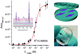
A microfluidic sensing device is fabricated by the integration of silver-coated porous silicon membranes as surface enhanced Raman scattering active nanostructures in a PDMS matrix showing plasmon resonances in the visible energy range. The membranes are shaped by defining a suitable pattern of the electrochemically etched silicon using the cover of the elastomeric chip. 4-Mercaptobenzoic acid, used as a probe molecule, shows Raman enhancement larger than 107 in electronic off-resonance conditions. The calibration of the SERS substrate is performed using a Langmuir isotherm fit, evidencing the analyte chemisorption. In order to check the potential of the chip as a multiplexed biosensing platform, model oligonucleotides (polyadenine, polyguanine, polythymine and polycytosine) are analyzed in a multichamber system.
Surface Enhanced Raman Scattering (SERS)-active substrates assembled as arrayed plasmonic elements can be exploited for these applications.5,6 They combine a multiplexing approach with the high sensitivity of the SERS technique taking advantage of a label free detection, which allows the minimization of the sample pre-treatments, in contrast to fluorescent microarray analysis. The analytes can be detected in trace concentrations and recognized through their vibrational fingerprints thanks to the Raman scattering enhancement provided by their interaction with nanostructured noble metal surfaces supporting localized surface plasmons (LPSs), without the need for any labeling steps.7
Recently, the microfluidic integration of SERS substrates has also attracted significant attention focused on chemical and biological analysis.8–10 Actually, the microfluidic set-up can solve problems involving a non-uniform molecular distribution on the SERS substrate surface and reduce the risks of sample contamination.11,12 Moreover, microfluidics can enable the in-flow synthesis of nanoparticles and dynamic detection benefiting from improved reaction kinetics with a limited reagent consumption. In-chip SERS analysis can finally exploit detection with portable Raman spectrometers, reducing instrumentation-related costs for point-of-care applications.
Solid SERS substrates are increasingly employed in microfluidic platforms due to their easier integration and increased stability with respect to colloidal nanoparticles, whose aggregation behavior in the fluidic channels has to be strictly controlled.13 Among them, silver coated porous silicon (Ag-pSi) has been previously studied for its high SERS sensitivity and wide plasmon resonance tunability.14,15 Because of the fabrication process, which involves the electrochemical etching of a silicon wafer in a HF electrolyte, followed by immersion plating in silver nitrate solutions,16,17 such structures have been so far used as “open SERS substrates”.
In this work, we present an easy fabrication method devoted to the preparation of a polydimethylsiloxane (PDMS) multi-chamber SERS-based microfluidic chip hosting Ag-coated porous silicon membranes (Ag-pSi). This device exploits features such as a low cost of fabrication, flexibility and optical transparency in the NIR-Vis energy range. pSi membranes featuring a suitable shape are etched through a thin PDMS mask and transferred onto a PDMS substrate. The silver nanoparticles are grown on the pSi-PDMS membranes on which a PDMS cover is finally bonded.
The optofluidic chip enables efficient and calibrated SERS analysis. In particular, a multianalyte detection configuration using different isolated chambers is here demonstrated for model oligonucleotides.
:
1 weight ratio, degassed at room temperature and cured in an oven at 60°. A 10
:
1 mixture was used for PDMS mask preparation. Porous silicon was etched starting from p+-type crystalline silicon18 (resistivity 34–40 mΩ cm) in a 20
:
20
:
60 water
:
hydrofluoric acid
:
ethanol solution. The current density and the anodization time were set to 30 mA cm−2 and 50 s in order to obtain the desired porosity and thickness of the porous layer. A 4
:
4
:
92 HF
:
H2O
:
ethanol solution was employed for the partial detachment of pSi membranes (etching time = 95 s, current density = 4 mA cm−2). The masking procedure and transfer of the membranes on PDMS are detailed in the Results and discussion section.
Specular reflectance spectra of the silvered samples were recorded in the 300–1200 nm range by means of a UV-Vis-NIR spectrophotometer (Agilent, Santa Clara, CA, USA) equipped with a 12.5° reflectance unit.
Raman measurements were performed using a Renishaw InVia Reflex micro-Raman spectrometer (Renishaw plc, Wotton-under-Edge, UK) with a 514.5 nm diode laser excitation using the multichamber chip in backscattering light collection. 5 mW laser power, 5 s of exposure time and 10 accumulations were employed to record each spectrum. 1 s exposure time and 2 accumulations were used instead for the mapping measurements.
4-Mercaptobenzoic acid (4-MBA), chosen as a SERS probe molecule, was diluted in ethanol at different concentrations and 2 μl of each solution was injected into the chambers. After static incubation for 30 minutes the solution was withdrawn with a micropipette and the chambers were washed with ethanol before the SERS measurement. 50 microns × 50 microns Raman maps (2.5 μm step) were acquired along the Ag-pSi membranes to average the 4-MBA signal intensity over a larger area in order to determine a calibration curve.
The silver nanoparticles are synthesized before the sealing of the device by dipping the pSi membranes bonded to the PDMS support in aqueous silver nitrate (Fig. 1h). Finally, the cover is aligned to the substrate and the bonding is achieved by adding a thin PDMS precursor mixture at the interface between the two components, followed by final crosslinking at 60 °C for 1 h. The fabricated device is characterized by four isolated chambers, including one silver-coated porous silicon membrane as the SERS active element, each equipped with inlet and outlet channels.
After immersion plating of the pSi-PDMS specimen in AgNO3, its surface is covered with silver nanoparticles, whose sizes are distributed with a certain polydispersion. Despite the irregular morphology, small inter-particle gaps of a few nanometers are distributed over all of the pSi membrane surface. Under light excitation, the electric near-field intensity can be huge within such nano-gaps, due to LSP coupling. This yields the well-known hot-spots, giving the highest Raman enhancements.23 Specular reflectance spectra of silver-coated pSi (Fig. 2b solid line) are consistent with the observed morphology, showing a very broad dip, covering a wavelength range of 400–800 nm, which arises from the convolution of many plasmon resonances ascribed to enhanced absorption/scattering processes related to LSPs coupled either to individual particles or through inter-particle interactions.
The SERS response of the chip is tested by employing 4-mercaptobenzoic acid (4-MBA), which is increasingly used as a probe molecule in SERS due to its non-resonant electronic behavior under the most common excitation conditions in the visible-NIR range.24,25 This can be easily demonstrated by the collection of a 4-MBA UV-Vis absorption spectrum, which is characterized by two intense bands at 217 and 270 nm (Fig. S4†). Raman measurements are therefore performed using a 514.5 nm laser, which provides an excitation within the plasmon band of the Ag-coated pSi membrane, while keeping off-electronic resonance conditions for the 4-MBA analyte.
Ag-pSi-PDMS samples are tested by filling the chambers of the optofluidic device with 4-MBA ethanolic solutions at increasing concentrations, starting from 10−9 M up to 10−2 M. Selected spectra are reported in Fig. 3a, while the whole series is provided in Fig. S5.† The 4-MBA vibrational fingerprint is dominated by the ν12 of the aromatic ring coupled with the C–S stretching at 1077 cm−1 and the ν8a ring mode at 1584 cm−1.26 These peaks can be already identified with a good signal-to-noise ratio after incubation with the 10−8 M solution. A pSi-PDMS chip sample without nanoparticles is also incubated with 4-MBA solution as a reference, without the final washing step to avoid the removal of the non-specifically adsorbed thiol. A 4-MBA signal cannot be detected until a 10−1 M concentration is reached, due to the absence of the plasmon enhancement giving a SERS regime. This measurement allows the calculation of the external amplified Raman efficiency14 (EARE) of the Ag-pSi-PDMS substrate, defined as the ratio of the minimum concentration of 4-MBA detectable on the Ag-coated sample to the one on the bare pSi-PDMS surface. Due to the complex morphology the estimation of the actual amount of adsorbed molecules is quite hard and the enhancement factor cannot be calculated. An EARE of ∼ 107 is derived, which can be essentially ascribed to the plasmonic resonant excitation of the Ag-pSi-PDMS SERS substrate.
The integrated area of the most intense peak (1584 cm−1) of 4-MBA as a function of the concentration is extracted by averaging the Raman signal using SERS maps in order to obtain a calibration curve. The Raman intensity data, which show a monotonic increase vs. the analyte concentration, can be successfully fitted by a Langmuir isotherm with a very good R2 value of 0.99. Actually, the Langmuir model only applies to equilibrium processes in which chemisorption of the analyte on a fixed number of binding sites occurs. This behavior is reasonable for 4-MBA whose thiol group is able to strongly bind to the silver surface.27 Saturation of the Raman signal at concentrations higher than 5 × 10⁻³ M can be also explained by the saturation of the surface adsorption sites.
The analyses here discussed imply that the chip can be calibrated and employed in quantitative analysis.
A pre-treatment of the cover with BSA is needed to avoid oligonucleotide adsorption on the PDMS walls, which exhibit a high affinity to the pyrimidine and purine fragments of the oligos.28
Polyadenine (polyA), polyguanine (polyG), polythymine (polyT) and polycytosine (polyC) solutions are prepared in a TE buffer and injected into the four chambers respectively. The SERS signal can be recorded sequentially under the 20× objective of the Raman microscope both with the chambers filled by the solutions and after solvent evaporation. A picture of the four-chamber chip used in the experiment is shown in Fig. 4b along with the spectra recorded at 514.5 nm after drying of the oligo solution (Fig. 4a).
![]() | ||
| Fig. 4 Multianalyte SERS. (a) SERS spectra of polyA, polyC, polyG and polyT in the four different chambers. (b) Picture of the optofluidic chip. | ||
The spectra are dominated by nucleobase modes, which preferably adsorb on the silver surface, while the backbone (OPO and PO2− stretching vibrations at 760, 830 and 1090 cm−1) and deoxyribose modes (870 and 1030 cm−1)29 are poorly visible. Taking into account previous experimental findings concerning the Raman detection of oligonucleotides by SERS colloidal systems or by TERS, the fingerprint of each sequence can be easily recognized. The polyA spectrum is characterized by its distinctive ring breathing at 730 cm−1 and the intense C–N stretching band at 1325 cm−1. The polyG can be recognized by a C–N ring stretching peak located at a higher Raman shift (1360 cm−1) and the intense 1480 cm−1 and 1580 cm−1 bands, attributed to C–N stretching/N–H bending and NH2 scissoring respectively.30 Pyrimidine based oligonucleotides show typical features around 790 cm−1 (6-member ring breathing) and 1640 cm−1 (carbonyl stretching). Moreover, the spectra can be distinguished by the different fingerprints in the 1200–1300 cm−1 range, where a doublet is observed for polyC at 1256–1305 cm−1, while a single peak at 1246 cm−1 represents the C–N stretching for polyT.31
It is worth underlining that the PDMS peaks expected as interfering features in the Raman spectra are not observed despite the elastomeric cover of the device being crossed twice by the excitation beam. This can be ascribed to the focusing of the excitation beam at the membranes surface, which provides the SERS enhancement close to the Ag nanoparticles.
Footnote |
| † Electronic supplementary information (ESI) available: Cover mold scheme, detailed fabrication scheme, FESEM cross section of the transferred pSi membrane, 4-MBA UV-Vis absorption spectrum, SERS spectra of 4-MBA at several concentrations. See DOI: 10.1039/c5ra26746c |
| This journal is © The Royal Society of Chemistry 2016 |