DOI:
10.1039/C4RA17052K
(Paper)
RSC Adv., 2015,
5, 26081-26091
Enhanced electrochemical performance of a lead–acid battery by a surface modified negative grid with multiwall carbon nanotube coating†
Received
25th December 2014
, Accepted 26th February 2015
First published on 26th February 2015
Abstract
High-performance lead–acid battery (LAB) negative grids have been prepared using a simple carbon nanotube (CNT) coating method. To assess the properties of these materials for use in LAB systems, galvanostatic charging–discharging measurements, electrochemical impedance spectroscopy (EIS) and cyclic voltammetry (CV) were performed. The morphology and chemical composition of the CNT coating on the negative grid have been investigated using scanning electron microscopy (SEM), Raman spectroscopy and energy dispersive spectrometry (EDS) characterization. The results clearly demonstrate that the CNT coating is uniform and fully covers the negative grid of the LAB, which acts as a CNT adhesion layer (CNTAL) between the current collector and the negative active materials (NAMs), and improves the electrical conductivity. Moreover, an enhanced charge acceptance, and excellent electrochemical performance and cycling stability have been observed for these CNT coated electrodes in comparison to the uncoated electrode. The obtained results reveal that the CNT coating not only reduces the charge transfer resistance but also protects the NAM from irreversible lead sulfation.
1. Introduction
Lead–acid batteries (LABs) have been highlighted as one of the most promising electrochemical energy storage devices for more than 150 years.1 Among the various secondary battery systems, LABs are still extensively used in automotive, power back up system, smart grid and stationary applications.2 The most important advantages of LABs are operational safety, the use of low-cost and highly abundant materials, easy construction and a well-recognized recycling technology, which makes them an appealing candidate for energy storage systems.3 In contrast, lithium-ion batteries (LIBs) power millions of laptop computers, electric vehicles and other portable electronics, despite that the Li material resource is limited in the Earth’s crust4,5 and a recycling process is technically elusive due to the different type of chemistry used in LIBs. At present less than 1% of lithium is recycled and the process costs more than five times that of the primary production of Li metal.6 Interestingly, LABs are more than adequate for many emerging energy storage applications and for a new generation of burgeoning advanced hybrid electric vehicle (HEV) batteries. Unfortunately, the reversibility of lead and lead dioxide active materials still remains a major issue. To overcome such pertinent technical challenges, their employment with various carbon-based conductive additives/materials is under focus.7–18 To date, all world-wide experimental data have indicated the presence of carbonaceous material in the active mass of the negative electrode based on structural affinity between the lead and carbon.19–22
In recent years, several reports demonstrated that it is possible to configure carbon-based inter/adhesive layers between the current collector and active material and the electrode and separator, which improves the cyclic performance of the lithium and sodium battery systems.23–32 Another attractive strategy is to improve the electrical conductivity and performance of supercapacitors, microbial fuel cells, solar cells and LIB electrodes by impregnating, using conductive wrapping,33 brush-coating,34 spraying35 or dipping36 techniques, with CNT ink/graphene based materials.37–40
Therefore, we adapted this approach for our LAB negative electrode, which gives a remarkable cycling performance. The primary function of grids is to provide an electrical contact between the positive and negative active materials, which serves to conduct the current. Additionally, the grid/active material interface plays a significant role in the determination of the positive active material (PAM) utilization.41,42 A very low electronic conductivity of the grid/active material interface hampered the PAM within the pellet and led to increased ohmic drop.43 These issues can be addressed through numerous approaches for making superior positive electrodes.44–51 On the other hand, the grid/NAM interface region, which is not discussed in the LAB normal cycling operations, is given minor importance in this region. However, in modern society with high rate cycling operations, this region (grid resistance) also plays a pivotal role in determining the performance of LABs.52 Furthermore, if this region does not have desirable conductivity it will impede the current flow, increase the ohmic drop and non-uniformity of the potential distribution across the grid, and promote hydrogen evolution, instead of transferring electrons to the NAM in high rate cycling.52,53
Though the NAM consists of primary (skeleton)/secondary (energetic) structures, these two structures play a most prominent role in negative plate operation. Moreover, the function of the energetic structure participates mainly in the processes of current generation, while the skeleton structure is the mechanical carrier of the energetic structure and conducts the electric current from the plate grid to every point of the NAM.54–56 Thus the grid/skeleton structure interface region might allow a high current with very low resistance if the NAM is in a fully discharged condition. Many of the earlier studies demonstrated improvement of the negative grid conductivity and uniformity of the active material utilisation by modification of the grid and tab designs.57,58 In another approach, light weight/conductive grids made from lead coated graphite,59 reticulated vitreous carbon (RVC),60 carbon/graphite foams61,62 or polyaniline63 coated negative electrodes were used. However, the introduction of these materials involves complex or unpractical manufacturing processes and often reduces the strength and electrochemical stability.
To address the main scientific issues, it is highly desirable to modify the negative grid material to meet the present day requirements. In this study, we present the feasibility and practicality of a surface treatment which involves CNTs being coated directly onto the negative grid of a LAB. This leads to a percolated structure even at low concentrations of CNTs, allowing a highly conductive negative grid to be made. The results demonstrate the use of a CNT coated negative grid as a new class of negative grid material for LAB applications.
2. Experimental section
2.1 Preparation of the CNT ink
CNTs, 40–50 nm in diameter and 5–15 μm in length with purity: >99%, purchased from SRL chemical Ltd were used. The CNT ink was prepared by adopting a reported method.36 The ink was prepared by dispersing a 1.6 mg mL−1 of CNTs in water with 10 mg mL−1 sodium dodecylbenzenesulfonate (SDBS) as the surfactant. After bath sonication for 5 min, the CNT dispersion was probe sonicated for 30 min to form an ink.
2.2 Cell fabrication
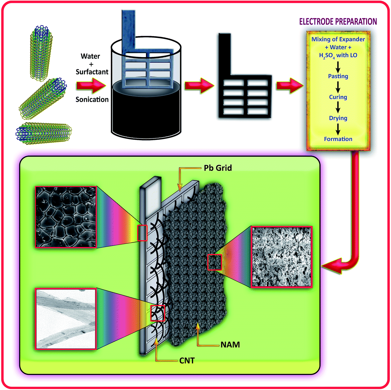
The preparation method for the positive and negative pastes has been reported previously.12 The plates were cured and formed as per conventional technologies.18,21 Here, we employ a conventional negative paste (0.25% carbon black, 0.3% lignin and 0.3% barium sulfate) as the active material to make the negative electrode, instead of using specialized carbaneous materials, to demonstrate that the observed improvement in cyclability is only contributed to by the CNT ink coating on the grid. The test cells were assembled with 1 negative (27 mm × 25 mm × 1.5 mm) and 2 oversized positive plates per cell, with a PVC separator. The grids were made from a lead–antimony–selenium alloy. The cells were filled with 30 mL of 1.26 sp gr sulphuric acid (H2SO4). The performance of the lead–acid cells was limited by the negative plate. Fig. 1 shows the simple and overall processes for the CNT coated lead grid and electrode preparation.
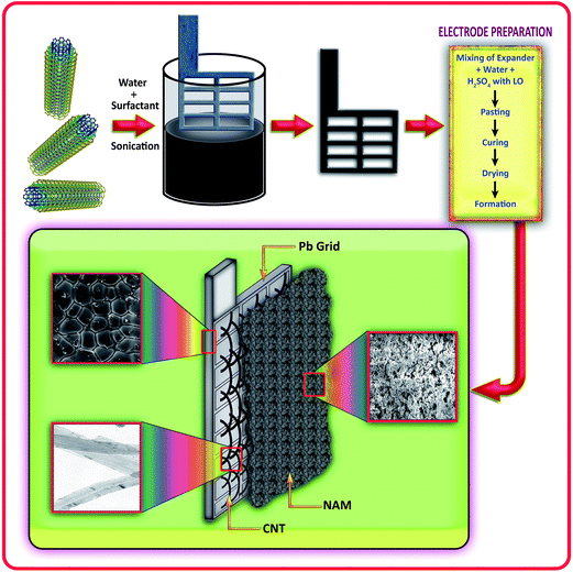 |
| | Fig. 1 Schematic representation of the overall processes for the CNT coated lead grid and electrode preparation. | |
3. Characterization techniques
The structures were characterized using scanning electron microscopy (SEM, TESCAN). Energy-dispersive spectroscopy (EDAX) images were also taken on the same apparatus used for SEM. The discharge–charge voltage profiles and cyclability data were collected using a programmable battery cycler (Bitrode) and the electrochemical behavior investigation was performed using an Auto lab electrochemical work station. The working electrode was a lead alloy strip (Tab portion of the grid) with a geometric area of 0.70 cm2. A platinum electrode with a large area was used as the auxiliary electrode. The reference electrode was Hg|Hg2SO4|1.28 g cm−3 H2SO4. All potentials in the cyclic voltammetry experiments are reported with respect to this reference electrode. Cyclic voltammetry was performed at a scan rate of 5 mV s−1 in the voltage window of −0.5 to −1.3 V. The electrochemical impedance spectroscopy (EIS) was performed in the frequency range of 10 mHz–100 kHz at an AC voltage of 5 mV. The EIS analysis was performed at six different potentials in a 1.28 sp gr H2SO4 solution at room temperature.
4. Results and discussion
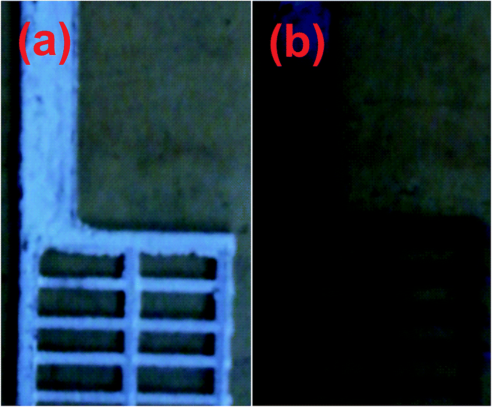
In Fig. 2a and b are shown the bare and as-prepared CNT coated lead alloy grids. The lead alloy negative grid was dipped into a black CNT ink. This dipping and drying cycle was repeated two times. The CNT coated grid was then placed in the vacuum oven for 10 min, drying at 100 °C, to remove any trapped water. After dipping into CNT ink, the grid shows a clear color change from white to black (Fig. 2b). Even at a very low concentration, the CNTs can serve as an efficient electron conducting network at the grid/NAM interface. Interestingly, during the dipping process most of the CNTs were observed on the surface of the grid, but some of the CNTs were located in the grain boundary as well as in voids of the Pb alloy. Fig. S1† shows the SEM and TEM images of pristine CNTs.
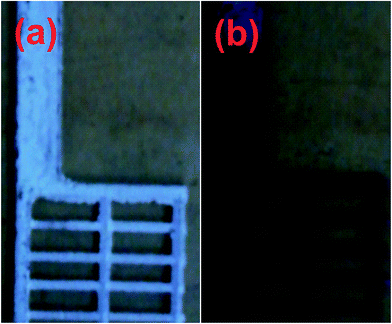 |
| | Fig. 2 Photographs of a representative bare (a) and CNT coated (b) lead alloy grid. | |
4.1 FT-Raman studies
Raman spectroscopy provides a powerful tool for analyzing the structural characterization of carbonaceous materials. Therefore, we performed Raman measurements for the lead alloy grids with and without the CNT coating to further confirm the presence of carbon in the grid. As shown in Fig. 3, the Raman spectrum of the CNT coated grid displays three prominent peaks at 1330, 1580 and 2630 cm−1, mainly corresponding to the D-band (disordered structured carbon), G-band (tangential stretch mode) and 2D-band (second order or overtone of the D-band), respectively.64 The graphitized carbon contains sp2 hybrid bonding, which is clearly correlated with the electronic conductivity of CNTs, and the disordered carbon mainly corresponds to sp3 hybrid bonding.65 No Raman peaks for carbon appear for the bare lead grid.
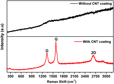 |
| | Fig. 3 Raman spectra of (a) a Pb grid and (b) a CNT coated Pb grid, using 632.8 nm diode laser excitation. | |
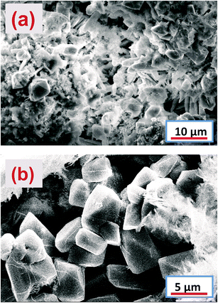
4.2 SEM of the Pb alloy with and without the CNT coating
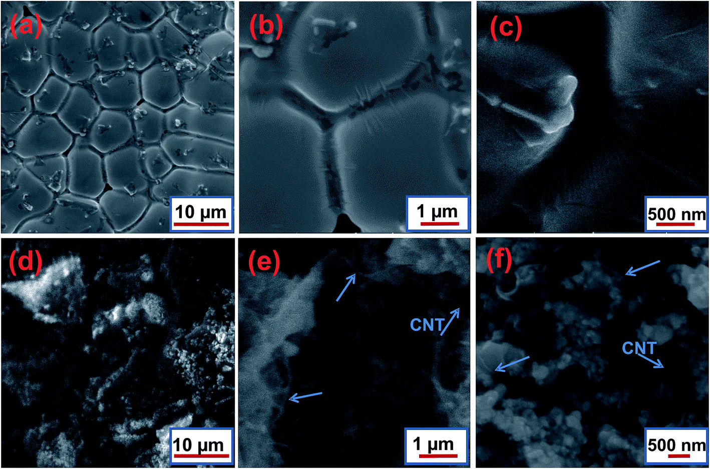
Fig. 4a–f show the scanning electron micrographs comparing the microstructure of the grids without and with a CNT coating. Fig. 4a shows the low magnification typical structure of the Pb–Sb–Se alloy. Fig. 4b and c, containing the grid without a CNT coating, indicate a very thin grain boundary layer, which is clearly visible. Meanwhile, for the CNT coated grid (Fig. 4d–f) this kind of grain boundary was embraced by the CNTs, which serves a dual function as both a conductive filler and also perhaps participating in the charging process through double layer formation. This effect may be involved in our cell, and the exact mechanism is unclear. Furthermore, a possible mechanism could be discussed in the CV/charge acceptance section. The typical micrographs in Fig. 4d–f clearly demonstrate that the CNTs were attached well to the grid, which is able to provide subtle surface contact. Hence, a relatively good dispersion of the CNTs on the surface of the grid is confirmed through SEM.
 |
| | Fig. 4 SEM images of the lead alloy grid (a–c) without and (d–f) with a CNT coating. | |
Moreover, it can be seen in Fig. 4e that an intimate contact between the grid and CNT exists, which will provide good electronic interactions between the grid and the NAM interface. This can probably be attributed to the relatively improved charge acceptance and conductivity. This is an indication that CNTs, with high conductivity, can provide an efficient electron transport pathway from the current collector to the skeleton structure of the NAM particles, thereby delivering enhanced capacity retention and rate capability. The morphology of the CNT coated grid is slightly changed by the CNT ink dipping process. The morphological changes are attributed to the presence of surfactant in the CNT ink. Interestingly, this morphology did not noticeably alter the electrochemical behavior of the CNT coated grid. Apparently, there are no additional prominent peaks or phases in the Raman or EDS measurements. For real applications, the grid surface being free from any residual surfactant is better; therefore, the coating method still needs to be improved in the future. In agreement with the above SEM findings, EDAX images further support the formation of uniform carbon on the CNT coated lead grid surface.
4.3 EDAX of the Pb alloy with and without the CNT coating
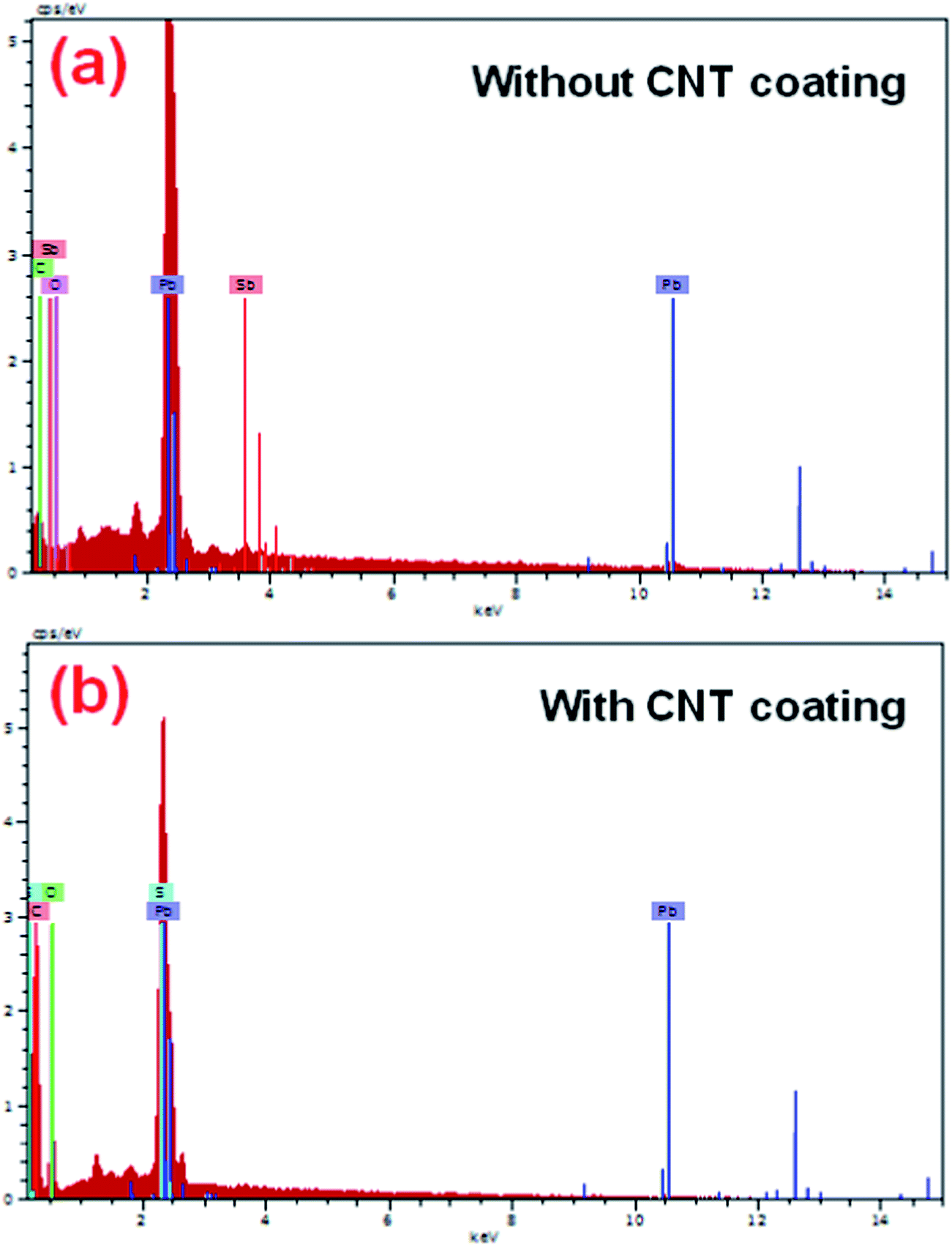
Fig. 5a and b show the EDS spectra of the grids with and without a CNT coating, before active mass pasting. Moreover, it is noteworthy to mention that the presence of a resilient carbon signal appeared along with a major amount of lead signal, which indicated that the CNTs are covered over the grid surface compared with the bare grid. However, no studies have been conducted so far on impregnating CNTAL in the negative grid of LABs.
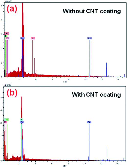 |
| | Fig. 5 EDAX spectroscopy of negative grids (a) without a CNT coating and (b) with a CNT coating. | |
5. Electrochemical properties
5.1 EIS study of the Pb alloy with and without the CNT coating
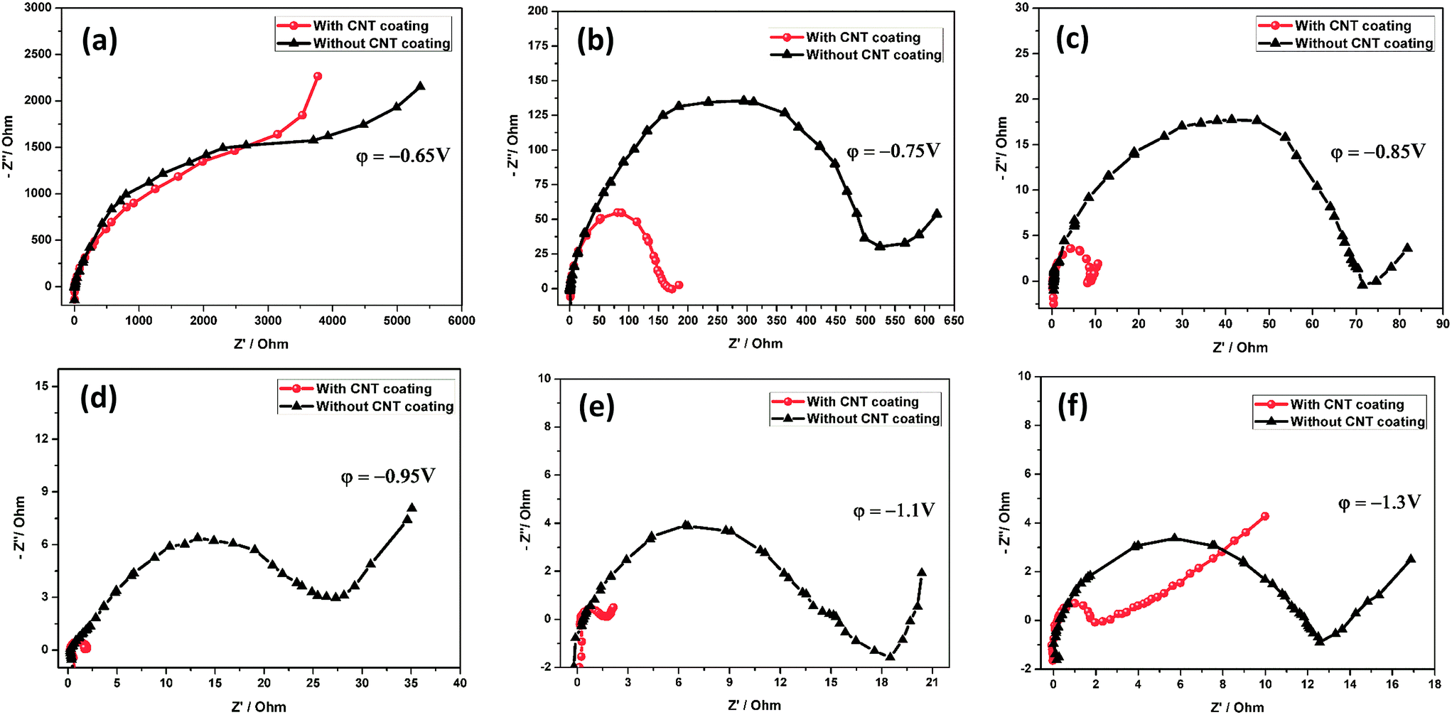
A detailed electrochemical impedance spectroscopy (EIS) analysis was performed at six different potentials in a 1.28 sp gr H2SO4 solution at room temperature on the grids with and without a CNT coating, as shown in Fig. 6a–f. As a pretreatment, 3 cycles from −0.6 V to −1.3 V were performed at a rate of 25 mV s−1. The tested electrodes were held at the required potentials for 15 min before the measurements. In this experiment, the electrode was subjected to a potential sweep from anodic to cathodic. The EIS technique has been employed to investigate the charge transfer processes occurring at electrode/solution interfaces. The semicircle is related to charge transfer resistance (Rct) and the straight line is ascribed to the Warburg impedance due to a diffusion process. It can be observed that the diameter of the semicircle related to charge transfer resistance decreases with subsequent cathodic potential regions, as shown in Fig. 6a–f. The Rct values were calculated by extrapolating the curve to a semicircle and then measuring the diameter of the semicircle.66 At the potential of −0.65 V, the grid surface consists of an outer PbSO4 layer. At the totally discharged potential of −0.65 V, Fig. 6a shows a high semicircle diameter, which presumably results in the formation of a PbSO4 layer over the grid surface. The Rct values do not vary much (∼4000 Ω), indicating that the insulating PbSO4 layer covered both the electrodes.
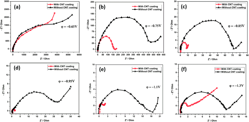 |
| | Fig. 6 Nyquist spectra obtained for the negative electrode with and without a CNT coating at various potentials. | |
The impedance behavior at −0.75 V shows a different type of semicircle, indicating an invariant interface between the bare and CNT coated grids (Fig. 6b). The decrease in the diameter of the semicircles could be due to a decrease in the contact resistance and passive layer thickness by CNT coating (Rct = 157 Ω). It is considered that the CNT coating plays a role in preventing the formation of dense/irreversible hard passive layer (PbSO4) reactions on the grid surface. It is obvious that there is also a sudden decrease of the Rct towards the cathodic potential window, as compared with the bare grid (Rct = 537 Ω). The same behavior has been observed for the potential ranges −0.85 V and −0.95 V. The Rct values are 8.7 and 1.8 Ω for the grid with a CNT coating, and 74 and 26 Ω for the grid without a CNT coating. This is a clear indication of the improvement in the conductivity of the CNT coated grid. At potentials of −0.93 V, reduction of PbSO4 to Pb starts. From Fig. 6c and d, it is reasonable to expect that the conductive CNT coating can accelerate fast electron transport between the negative grid and the PbSO4 layer. Moreover, this conductive CNT coating offers additional electron pathways.
At the cathodic potential (−1.1 V), the CNT coated grid and bare grid exhibited impedances of 1.42 and 14.01 Ω, respectively, as clearly demonstrated in Fig. 6e. A sharp decrease in the Rct of the CNT coated electrode occurred upon reaching the cathodic region, which may be associated with the largest electrochemically active surface area due to the incorporation of conducting CNTs on the grid surface and complete conversion of PbSO4 to Pb. Moreover, in the potential region between −0.93 V and −1.3 V, a reaction of Pb2+ reduction to Pb proceeds. This may suggest that the CNTAL can help to decrease the Rct towards the cathodic process. Fig. 6f shows a clear semicircle loop, indicating the high Rct of the bare grid (11.7 Ω). This result suggests that at this potential (−1.3 V) a tiny amount of irreversible PbSO4 film is still present on the bare electrode surface. Conversely, the CNT coated electrode shows a very small semicircle loop (1.1 Ω). It is evident that the charge transfer resistance is much lower at this interface. The data exhibited that the electrode impedance continued to decrease during the cathodic sweep process, suggesting that the CNTAL gradually increased the electronic conductivity of the negative electrode.
5.2 Cyclic voltammetry (CV) study of the negative grid with and without the CNT coating
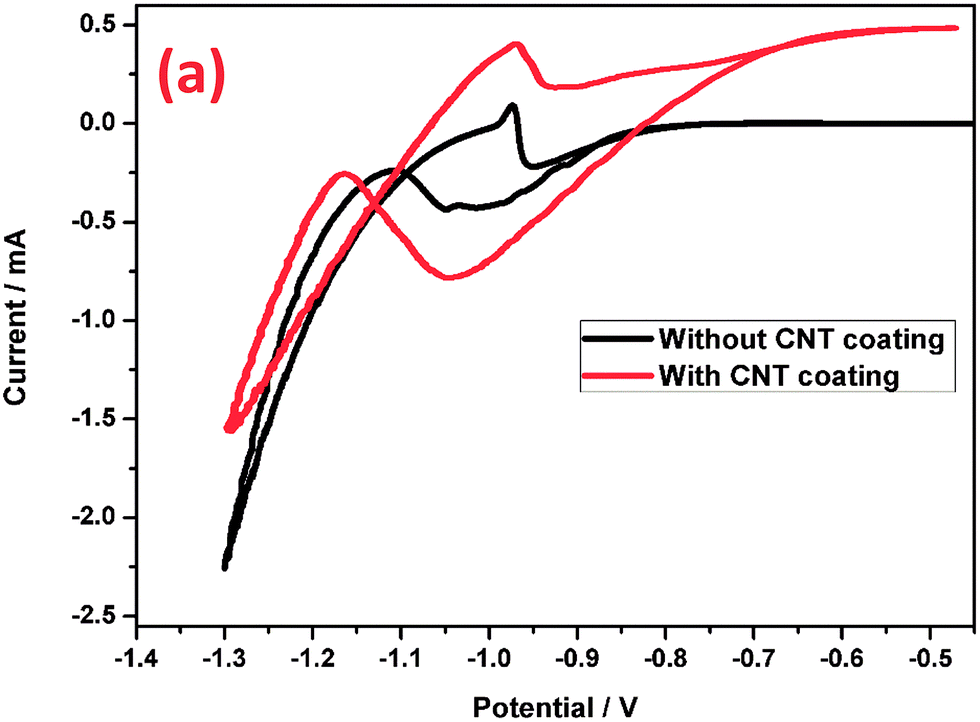
In order to confirm the electrochemical behavior of the grids with and without a CNT coating, cyclic voltammograms (Fig. 7) in the potential range from −0.5 to −1.3 V at a scan rate of 5 mV s−1 were recorded. The cyclic voltammograms of these two electrodes have very distinctly shaped curves, and clear electrocatalytic behavior could be observed in the potential range, which was correlated with enhanced electron transfer rates and increased currents. In the anodic sweep, the potential region between −0.93 V and −0.7 V, Pb is oxidized to PbSO4. Meanwhile in the cathodic sweep, the formed PbSO4 was reduced to spongy Pb at −0.95 V to −1.11 V. The peak current value of the CNT coated electrode is much higher than that of the bare electrode, which means that in addition to a faradaic contribution, the CNTs might also contribute through electric double layer formation. Moreover, the non-faradaic current for the CNT coated electrode is significantly larger than that of the bare electrode, possibly due to the high surface area of the CNTs. Moreover, the oxidation of Pb and reduction of PbSO4 could proceed through the CNTAL, which improves the reversibility of the negative electrode. It is generally believed that CNTs possess an ideal capacitive behavior in aqueous solution due to the presence of protons which are involved in the charge storage reaction. The CNT coated grid stores energy using a non-faradaic double layer formation and also due to faradaic pseudo-capacitive processes such as the intercalation reaction of hydrogen, which eventually improves the charge acceptance.67 Hence, this study reveals that the CNTAL on the grid surface may have a prominent role in improving the efficiency of the LAB negative electrode performance by enabling a combination of faradaic and non-faradaic reactions. This is also potentially one of the reasons for the improved reversibility of the negative electrode. The results of the CV studies are in agreement with the impedance studies. Hence, in the case of the grid without the CNT coating, energy is stored using a conventional faradaic process of lead to lead sulfate. Our result found similarity with earlier reports by Pavlov et al. on their study of lead–carbon model electrodes.9,68
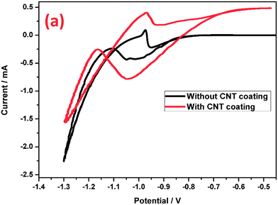 |
| | Fig. 7 Cyclic voltammograms of the negative grids with and without a CNT coating. | |
6. Charge–discharge cycling
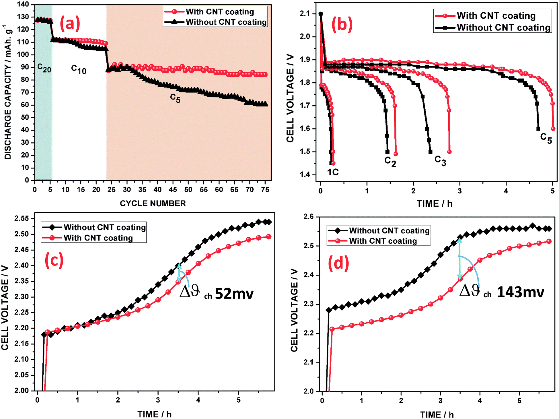
In order to determine the nominal capacity of the cell after its formation, the cell was subjected to five charge–discharge cycles (20 h of discharging mode, 0.05C). Subsequently, the cell was subjected to C10 (18 cycles) and C5 (57 cycles) conditions, as shown in Fig. 8a. Based on the experimental results, it was indicated that a low rate cycling performance has no significant change on the discharge capacity. Further, the discharge capacity (C5) of the CNT coated grid cell was stabilized at a level of 89 mA h g−1 and stayed around this value with minor fluctuations for up to 57 cycles. Upon increasing the cycle number, the cell of the grid without the CNT coating reflected a poor capacity retention, which may be due to the formation of irreversible PbSO4 phases during the cycling and its subsequent electrical isolation from the grid. Consequently, the poor electron transport across the grid/NAM interlayer contributes to a high charge transfer resistance and overpotential. It has been understood that the CNT coating is able to enhance the charge process and make the charge–discharge reactions more reversible.
 |
| | Fig. 8 (a) Cycling performance, (b) discharge curves at different current densities, (c) charge curves for the 3rd cycle and (d) 15th cycle (C5 rate). | |
The rate capabilities are compared for the two cells in the discharging sequence in Fig. 8b. Under all high discharge current densities, it can be seen that the discharge capacities of the CNT coated electrode cell are substantially larger than those of the electrode cell without the CNT coating. These results show that the negative electrode with the CNT coating displayed improved rate capability. Moreover, the discharge voltage profiles, as can be seen from Fig. 8b, reveal that the contact resistance at the grid/NAM particles has a strong effect on the rate performance.
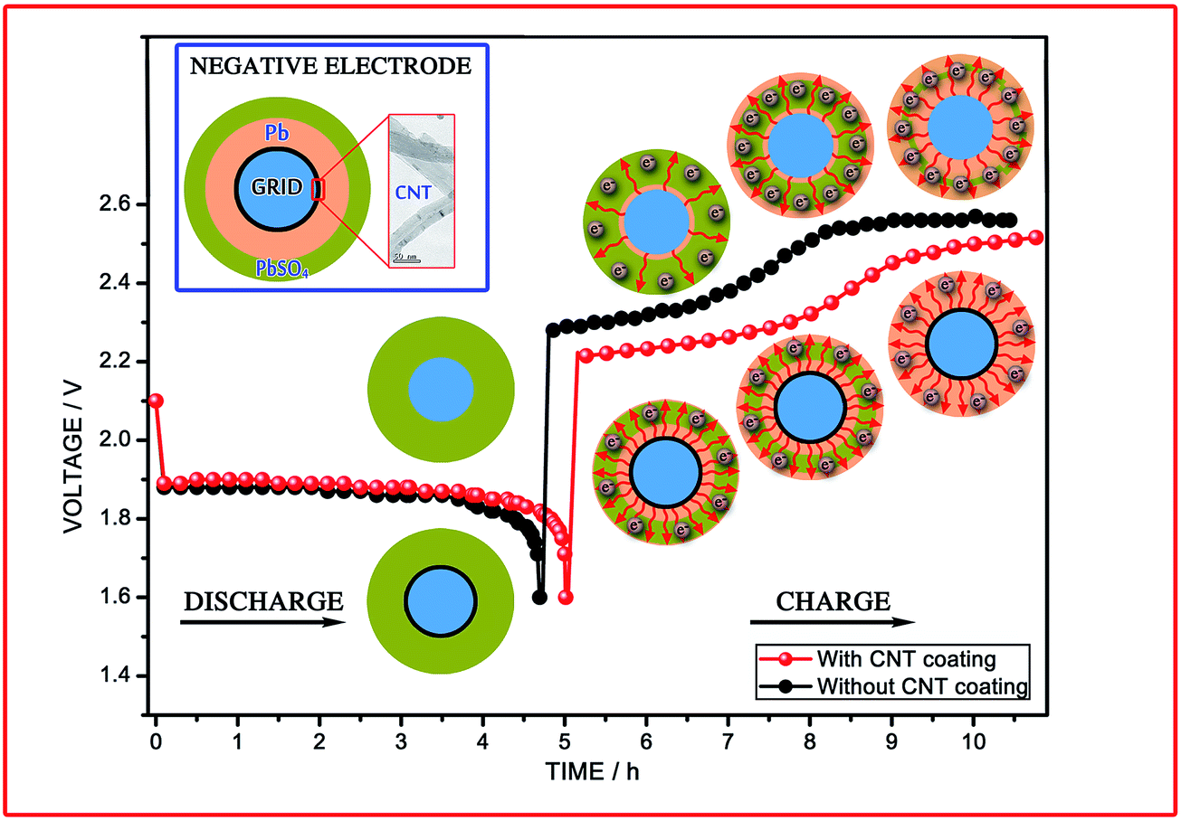
Fig. 8c and d show the charging (C5) voltage profiles of the cells. From Fig. 8c, it can be seen that the charge voltages of both cells were very close to each other. Furthermore, in the 15th cycle of the C5 rate, the potential of the uncoated grid cell is shifted 143 mV higher than that of the CNT coated grid cell even before attaining 65% of SoC, which can be clearly seen in Fig. 8d. Moreover, this behavior indicates that the hydrogen gassing potential was also postponed when the CNTAL coating was incorporated onto the negative grid and that the CNT coating could increase hydrogen adsorption and storage on the surface of the CNTs.69,70 This indicates that the electrochemical reaction of Pb2+ reduction on the Pb surface proceeds at a much lower potential at the Pb + CNT/electrolyte interface. This behavior is mainly attributed to the CNT coating reducing the polarization of the negative electrode, which accelerates the charge processes, though the discharge products are covered on the Pb grid, which can easily form an insulating layer (PbSO4) on the grid/active mass surfaces. In subsequent high rate cycling, the insulating layer on the Pb surface would accumulate further. Hence, this also proves that the electrons flowing from the grid towards the surface of the NAM reduce some hydrogen ions to H2 gas prior to reacting with the PbSO4 layer, which will result in fast polarization, as is clearly revealed in Fig. 8d. This may possibly be attributed to the 15th charging plateau, which is higher than the voltage of the third charging process, in the grid cell without the CNT coating.
6.1 Charge acceptance test
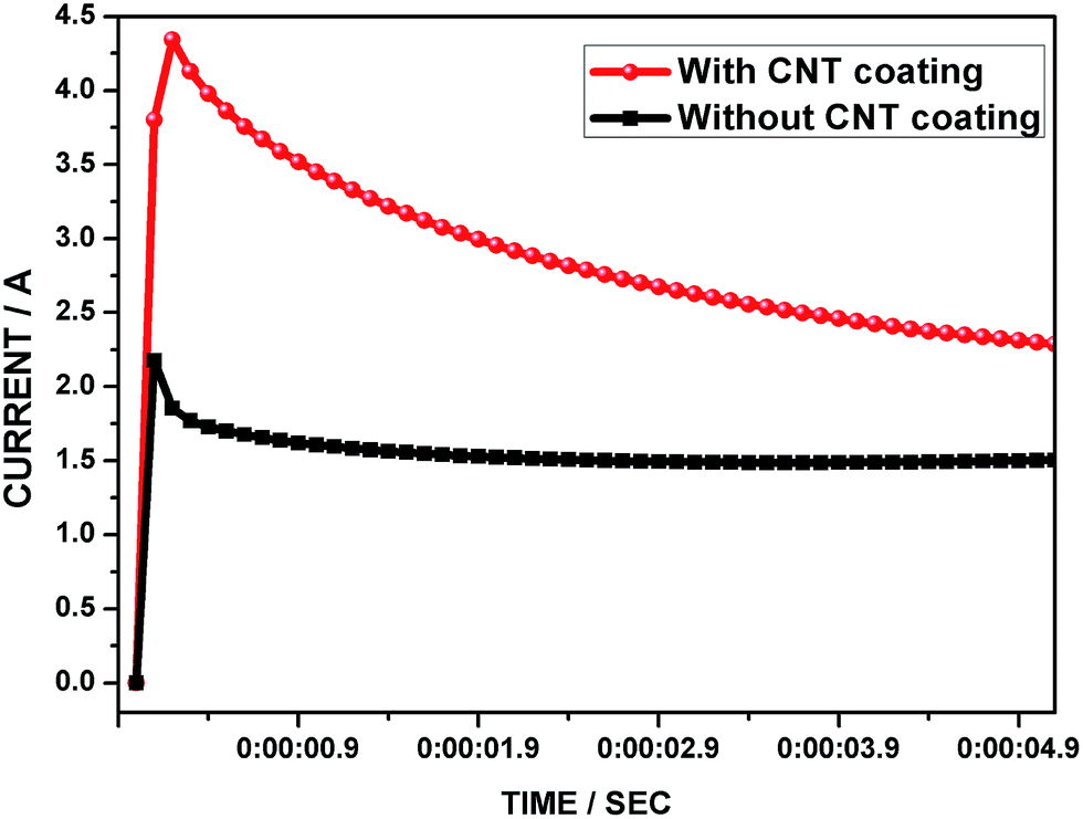
In order to understand the effects of CNT coating on the lead grid, the cell was subjected to charge acceptance tests. In modern LAB operation, the high rate charging which is required in HEV applications (for regenerative braking) is usually only for a few seconds. In this study, the test cells were subjected to 5 s of the high rate charge with an upper voltage limit of 2.55 V.12 Fig. 9 shows a comparison of the charge acceptance curves for the lead electrode cells with and without the CNT coating. Furthermore, the CNT coated lead electrode cell reached a higher threshold current compared with the control cell. This indicates that the CNTs are playing a seminal role in the charge processes, apart from the electroconductivity effects in enriching the electron transfer kinetics. Interestingly, the CNTAL considerably increases the value of the average double layer current at the beginning of the charge. For clearer understanding, the negative electrode has a typical double-layer capacitance of 0.4–1.0 F A h−1,52 which is not suitable for absorbing short and sharp charge currents. In the present work, the CNTAL contributes to increasing the electrochemical active surface area as well as double layer capacitance. Apart from this, the current that flows through the negative grid initially due to the electric double layer reaction, which is mainly charged in the first moment of a high current pulse, completely reduces the PbSO4 in the grid surface and facilitates a high rate of electron transport to the skeleton structure of the NAM. After a short time, the whole current flows through the faradaic reaction because only a very thin layer of CNTs is coated on the Pb grid surface. This is in tune with a very recent report by Pavlov et al., where they showed that charging and discharging of the electric double layer might proceed very quickly on the electrode surface, and proceeds mainly within the first five second pulse.22 It is worth mentioning that, the charge transfer resistance of the Pb/H2SO4 interface is high in comparison with the Pb + CNT/H2SO4 interface, which can facilitate a much higher current flow in this region. This correlation is supported by the impedance results demonstrated in Fig. 6.
 |
| | Fig. 9 Charge acceptance curves of the negative electrode cells with and without the CNT coating. | |
Fig. 10 presents a schematic of the discharging–charging of the LAB as well as a tentative mechanism for the electron transfer pathways in the negative electrode. The cycle life of the LAB is determined by the reversibility of the processes that proceed during discharge–charge.71 Thus, the low charge acceptance of the electrode without the CNT coating, which leads to a significant amount of unreduced PbSO4 in the NAM, is clearly confirmed at the end of the charge process. The first elementary process in the negative electrode during charging is the dissolution (chemical reaction) of PbSO4 crystals, which has a direct impact on the H2SO4 concentration and several other factors (PbSO4 → Pb2+ + SO42−). Therefore, combining all of the disputes discussed above, we prudently clarify the discharging–charging process of the CNTAL electrode (Fig. 10), which can help us to understand the actual movement of the electrons and the reversibility of the NAM. As shown in Fig. 10, since a boundless number of electrons can be obtained from the CNTAL at the beginning of the charge, this facilitates the deposition process (electrochemical reaction) being much easier (Pb2+ +2e− → Pb). The CNT coated grid, with its high electrical conductivity, leads to a higher electron density between the skeleton structure and current collector. Besides that, this model also helps us to understand how the CNTAL could significantly eliminate large polarization at an early stage of the high rate charge process. Moreover, the CNTs have a high surface area, and this will lower the polarization of the negative electrodes.
 |
| | Fig. 10 Schematic showing the discharge–charge reaction in LABs and a tentative mechanism for the electron flow/pathways in the negative electrode. | |
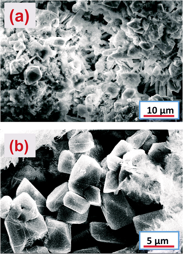
7. Scanning electron microscopy of the NAM after charge–discharge cycles
The morphology of the cycled NAM was revealed using SEM, as shown in Fig. 11. The SEM image of the CNT coated grid cell NAM particles clearly reveals the typical morphology of lead and a tiny amount of lead sulfate with agglomeration (Fig. 11a). Moreover, the NAM with small PbSO4 crystals would have a lower ion transfer resistance, which allows the diffusion kinetics to be much easier. Hence, it is presumed that such a type of morphology should enhance the electrochemical performance. From the above observations, we can conclude that the CNTAL serves as a conductive medium for the electron transfer process and maintains the contact between the NAM particles during the discharge–charge process. Thus, the CNT coating can act as a buffer zone and hamper the formation of irreversible lead sulfation during charge–discharge cycling. It was found that without the CNT coating, the electrode cell NAM was fully covered with PbSO4 particles, as shown in Fig. 11b. This type of PbSO4 cannot, or can only partially, be reconverted back to an electrochemically active form. This leads to rapid accumulation of PbSO4 on the negative plate, leading to early failure of the LAB.
 |
| | Fig. 11 SEM images of the grid cell NAM with (a) and without (b) the CNT coating. | |
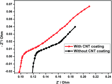
8. Impedance measurements
The AC impedance results obtained from the assembled test cells after 30 cycles are shown in Fig. 12. The semicircles in the Nyquist plots are depressed, which may be due to the changes in the resistive and capacitive components of the electrode/electrolyte interface, with respect to electrode position, electrode nonuniform thickness, etc.12 It is well known that a small Rct can provide a logical explanation for the increased rate performance of the CNT coated negative electrode in comparison with the uncoated electrode at higher rates (Fig. 12). The data exhibited that for the cell without the CNT coating, the impedance value increases during the cycling process, suggesting that the irreversible PbSO4 gradually decreased the electronic conductivity of the negative electrode.
 |
| | Fig. 12 Electrochemical impedance spectra of the lead–acid cell (after 30 cycles). | |
9. Conclusion
In summary, we have demonstrated a generalized strategy for the surface modification of a negative grid using a CNT coating. The CNT coating allows excellent electronic conductivity, excellent contact through the Pb grid to the skeleton structure of the NAM, and may also serve as a barrier against irreversible lead sulfation and capacity loss. These CNT coated grid cells have been cycled, even at high rates, with low capacity fading. At the same time, the CNT coating helped to overcome the issue of the inherent electrical resistance associated with the Pb/PbSO4 redox couple. Thus, based on our experimental results, we firmly believe that a CNT coating can obviously enhance the electronic conductivity of a negative electrode material. This CNT coating technique offers benefits for high performance and such coating methods are becoming increasingly important in the development of LABs. A charge–discharge test revealed that at a high current rate, the grid using a CNT coating had a better rate performance and its capacity faded much less, than when using a bare grid. This approach offers a new way to introduce a surface coating (CNTs) to the negative grid in LABs and could potentially become applicable for various designs of the cell configuration, e.g., the surface of the NAM, PAM and separator materials. The extension of this new surface coating approach to various carbon/nanostructured materials is the subject of ongoing investigations.
Acknowledgements
The authors are thankful to the Council of Scientific and Industrial Research (CSIR), India for the support to carry out this work.
References
- G. Plante, Acad. Sci., Paris, C. R., 1860, 50, 640–642 Search PubMed.
- J. Pan, Y. Sun, W. Li, J. Knight and A. Manthiram, Nat. Commun., 2012, 4 DOI:10.1038/ncomms3178.
- J. Garche, Phys. Chem. Chem. Phys., 2001, 3, 356–367 RSC.
- C. X. Zu and H. Li, Energy Environ. Sci., 2011, 4, 2614–2624 CAS.
- M. Armand and J. M. Tarascon, Nature, 2008, 451, 652–657 CrossRef CAS PubMed.
- Lead-based battery technologies are sustainable for the long-term, says a new study: http://www.doerun.com/Portals/0/ILA%20Battery%20study%20release%20FINAL.pdf.
- K. Nakamura, M. Shiomi, K. Takahashi and M. Tsubota, J. Power Sources, 1996, 59, 153–157 CrossRef CAS.
- M. Shiomi, T. Funato, K. Nakamura, K. Takahashi and M. Tsubota, J. Power Sources, 1997, 64, 147–152 CrossRef CAS.
- D. Pavlov, T. Rogachev, P. Nikolov and G. Petkova, J. Power Sources, 2009, 191, 58–75 CrossRef CAS PubMed.
- M. Fernandes, J. Valenciano, F. Trinidad and N. Munos, J. Power Sources, 2010, 195, 4458–4469 CrossRef PubMed.
- D. Pavlov, P. Nikolov and T. Rogachev, J. Power Sources, 2010, 195, 4435–4443 CrossRef CAS PubMed.
- M. Saravanan, M. Ganesan and S. Ambalavanan, J. Power Sources, 2014, 251, 20–29 CrossRef CAS PubMed.
- D. P. Boden, D. V. Loosemore, M. A. Spense and T. D. Wojcinski, J. Power Sources, 2010, 195, 4470–4493 CrossRef CAS PubMed.
- D. Pavlov, P. Nikolov and T. Rogachev, J. Power Sources, 2011, 196, 5155–5167 CrossRef CAS PubMed.
- R. Shapira, G. D. Nessim, T. Zimrin and D. Aurbach, Energy Environ. Sci., 2013, 6, 587–594 CAS.
- B. Hong, L. Jiang, H. Xue, F. Liu, M. Jia, J. Li and Y. Liu, J. Power Sources, 2014, 270, 332–341 CrossRef CAS PubMed.
- L. Zhao, W. Zhou, Y. Shaob and D. Wang, RSC Adv., 2014, 4, 44152–44157 RSC.
- S. M. Kumar, S. Ambalavanan and S. Mayavan, RSC Adv., 2014, 4, 36517–36521 RSC.
- S. Logeshkumar and R. Manoharan, Electrochim. Acta, 2014, 144, 147–153 CrossRef CAS PubMed.
- B. Hong, X. Yu, L. Jiang, H. Xue, F. Liu, J. Li and Y. Liu, RSC Adv., 2014, 4, 33574–33577 RSC.
- M. Saravanan, P. Sennu, M. Ganesan and S. Ambalavanan, J. Electrochem. Soc., 2013, 160, A70–A76 CrossRef CAS PubMed.
- D. Pavlov and P. Nikolov, J. Power Sources, 2013, 242, 380–399 CrossRef CAS PubMed.
- S. Lee and E. S. Oh, J. Power Sources, 2013, 244, 721–725 CrossRef CAS PubMed.
- Z. Zhang, Z. Zhang, X. Wang, J. Li and Y. Lai, J. Appl. Electrochem., 2014, 44, 607–611 CrossRef CAS.
- C. Zu, Y.-S. Su, Y. Fu and A. Manthiram, Phys. Chem. Chem. Phys., 2013, 15, 2291–2297 RSC.
- Y. S. Su and A. Manthiram, Nat. Commun., 2013, 3 DOI:10.1038/ncomms2163.
- Y. S. Su and A. Manthiram, Chem. Commun., 2012, 48, 8817–8819 RSC.
- S. H. Chung and A. Manthiram, Chem. Commun., 2014, 50, 4184–4187 RSC.
- X. Yu and A. Manthiram, ChemElectroChem, 2014, 1, 1275–1280 CrossRef CAS.
- Z. Zhang, Z. Zhanga, K. Zhanga, X. Yanga and Q. Lia, RSC Adv., 2014, 4, 15489–15492 RSC.
- F. Qin, K. Zhang, J. Fang, Y. Lai, Q. Li, Z. Zhang and J. Li, New J. Chem., 2014, 38, 4549–4554 RSC.
- X. Wang, Z. Wang and L. Chen, J. Power Sources, 2013, 242, 65–69 CrossRef CAS PubMed.
- G. Yu, L. Hu, N. Liu, H. Wang, M. Vosgueritchian, Y. Yang, Y. Cui and Z. Bao, Nano Lett., 2011, 11, 4438–4442 CrossRef CAS PubMed.
- D. Y. Cho, K. Eun, S. H. Choa and H. K. Kim, Carbon, 2014, 66, 530–538 CrossRef CAS PubMed.
- H. T. Jeonga, B. C. Kimb, R. Gorkina, M. J. Higginsa and G. G. Wallacea, Electrochim. Acta, 2014, 137, 372–380 CrossRef PubMed.
- L. Hu, M. Pasta, F. L. Mantia, L. Cui, S. Jeong, H. D. Deshazer, J. W. Choi, S. M. Han and Y. Cui, Nano Lett., 2010, 10, 708–714 CrossRef CAS PubMed.
- H. Y. Tsai, C. C. Wub, C. Y. Leec and E. P. Shiha, J. Power Sources, 2009, 194, 199–205 CrossRef CAS PubMed.
- S. G. Hashmi, J. Halme, Y. Ma, T. Saukkonen and P. Lund, Adv. Mater. Interfaces, 2014, 1, 1300055–1300060 Search PubMed.
- W. W. Liu, X. B. Yan, J. W. Lang, C. Penga and Q. J. Xue, J. Mater. Chem., 2012, 22, 17245–17253 RSC.
- J. Hou, Z. Liu, S. Yang and Y. Zhou, J. Power Sources, 2014, 258, 204–209 CrossRef CAS PubMed.
- D. Pavlov, J. Power Sources, 1995, 53, 9–21 CrossRef CAS.
- R. J. Ball, R. Kurian, R. Evans and R. Stevens, J. Power Sources, 2002, 111, 23–38 CrossRef CAS.
- A. F. Hollenkamp, K. K. Constanti, M. J. Koop, L. Apiiteanu, M. Calabek and K. Micka, J. Power Sources, 1994, 48, 195–215 CrossRef CAS.
- S. Zhong, H. K. Liu, S. X. Dou and M. S. Kazaco, J. Power Sources, 1996, 59, 123–129 CrossRef CAS.
- I. Kurisawa, M. Shiomi, S. Ohsumi, M. Iwata and M. Tsubota, J. Power Sources, 2001, 95, 125–129 CrossRef CAS.
- M. Cruz, L. Hernan, J. Morales and L. Sanchez, J. Power Sources, 2002, 108, 35–40 CrossRef CAS.
- G. Barkleit, A. Grahl, M. Maccagni, M. Olper, P. Scharf, R. Wagner and H. Warlimont, J. Power Sources, 1999, 78, 73–78 CrossRef CAS.
- K. Ji, C. Xu, H. Zhao and Z. Dai, J. Power Sources, 2014, 248, 307–316 CrossRef CAS PubMed.
- R. Demarco, A. Rochliadi and J. Jones, J. Appl. Electrochem., 2001, 31, 953–959 CrossRef CAS.
- K. Yamada, K. I. Maeda, K. Sasaki and T. Hirasawa, J. Power Sources, 2005, 144, 352–357 CrossRef CAS PubMed.
- W. H. Kao, S. L. Haberichter and K. R. Bullock, J. Electrochem. Soc., 1992, 139, L105–L107 CrossRef CAS PubMed.
- P. T. Moseley, D. A. J. Rand and B. Monahov, J. Power Sources, 2012, 219, 75–79 CrossRef CAS PubMed.
- L. T. Lam, N. P. Haigh, C. G. Phyland and T. D. Huynh, J. Power Sources, 2005, 144, 552–559 CrossRef CAS PubMed.
- V. Iliev and D. Pavlov, J. Appl. Electrochem., 1985, 15, 39–52 CrossRef CAS.
- D. Pavlov and S. Ignatova, J. Appl. Electrochem., 1987, 17, 715–723 CrossRef CAS.
- D. Pavlov and V. Iliev, J. Power Sources, 1982, 7, 153–164 CrossRef CAS.
- M. Calabek, K. Micka, P. Baca and P. Krivak, J. Power Sources, 2000, 85, 145–148 CrossRef CAS.
- P. Krivak, P. Baca, M. Calabek, K. Micka and P. Kral, J. Power Sources, 2006, 154, 518–522 CrossRef CAS PubMed.
- B. Hariprakash and S. A. Gaffoor, J. Power Sources, 2007, 173, 565–569 CrossRef CAS PubMed.
- A. Czerwinski, S. Obrebowski and Z. Rogulski, J. Power Sources, 2012, 198, 378–382 CAS.
- Y. Chen, B. Z. Chen, L. W. Ma and Y. Yuan, Electrochem. Commun., 2008, 10, 1064–1066 CrossRef CAS PubMed.
- Y.-I. Jang, N. J. Dudney, T. N. Tiegs and J. W. Klett, J. Power Sources, 2006, 161, 1392–1399 CrossRef CAS PubMed.
- S. K. Martha, B. Hariprakash, S. A. Gaffoor and A. K. Shukla, J. Appl. Electrochem., 2006, 36, 711–722 CrossRef CAS.
- M. S. Dresselhaus, A. Jorio, M. Hofmann, G. Dresselhaus and R. Saito, Nano Lett., 2010, 10, 751–758 CrossRef CAS PubMed.
- C. S. Rout, A. Kumar, T. S. Fisher, U. K. Gautam, Y. Bandoc and D. Golberg, RSC Adv., 2012, 2, 8250–8253 RSC.
- S. C. Raghu, M. Ulaganathan, T. M. Lim and M. S. Kazacos, J. Power Sources, 2013, 238, 103–108 CrossRef PubMed.
- M. Saravanan, M. Ganesan and S. Ambalavanan, J. Electrochem. Soc., 2012, 159, A452–A458 CrossRef CAS PubMed.
- D. Pavlov, P. Nikolov and T. Rogachev, J. Power Sources, 2010, 195, 4444–4457 CrossRef CAS PubMed.
- S. W. Swogger, P. Everill, D. P. Dubey and N. Sugumaran, J. Power Sources, 2014, 261, 55–63 CrossRef CAS PubMed.
- N. Sugumaran, P. Everill, S. W. Swogger and D. P. Dubey, J. Power Sources, 2015, 279, 281–293 CrossRef CAS PubMed.
- D. Pavlov and P. Nikolov, J. Electrochem. Soc., 2012, 159, A1215–A1225 CrossRef CAS PubMed.
Footnotes |
| † Electronic supplementary information (ESI) available. See DOI: 10.1039/c4ra17052k |
| ‡ Present address: Flour Milling, Baking and Confectionery Technology Department, CSIR-Central Food Technological Research Institute, Mysore-570020, India. |
|
| This journal is © The Royal Society of Chemistry 2015 |