
 Open Access Article
 This Open Access Article is licensed under a
 Creative Commons Attribution 3.0 Unported Licence
All-polymer photonic sensing platform based on whispering-gallery mode microgoblet lasers
T.
Wienhold
*a,
S.
Kraemmer
b,
S. F.
Wondimu
a,
T.
Siegle
b,
U.
Bog
ac,
U.
Weinzierl
d,
S.
Schmidt
d,
H.
Becker
d,
H.
Kalt
b,
T.
Mappes
ae,
S.
Koeber
af and
C.
Koos
*af
aInstitute of Microstructure Technology (IMT), Karlsruhe Institute of Technology (KIT), 76128, Karlsruhe, Germany. E-mail: tobias.wienhold@kit.edu; christian.koos@kit.edu
bInstitute of Applied Physics (APH), Karlsruhe Institute of Technology, 76128 Karlsruhe, Germany
cNow with Institute of Nanotechnology (INT), Karlsruhe Institute of Technology, 76128 Karlsruhe, Germany
dMicrofluidic ChipShop GmbH, 07747 Jena, Germany
eNow with Carl Zeiss AG, Corporate Research and Technology, 07745 Jena, Germany
fInstitute of Photonics and Quantum Electronics (IPQ), Karlsruhe Institute of Technology, 76128 Karlsruhe, Germany Web: http://www.ipq.kit.edu
First published on 12th August 2015
Abstract
We present an all-polymer photonic sensing platform based on whispering-gallery mode microgoblet lasers integrated into a microfluidic chip. The chip is entirely made from polymers, enabling the use of the devices as low-cost disposables. The microgoblet cavities feature quality factors exceeding 105 and are fabricated from poly(methyl methacrylate) (PMMA) using spin-coating, mask-based optical lithography, wet chemical etching, and thermal reflow. In contrast to silica-based microtoroid resonators, this approach replaces technically demanding vacuum-based dry etching and serial laser-based reflow techniques by solution-based processing and parallel thermal reflow. This enables scaling to large-area substrates, and hence significantly reduces device costs. Moreover, the resonators can be fabricated on arbitrary substrate materials, e.g., on transparent and flexible polymer foils. Doping the microgoblets with the organic dye pyrromethene 597 transforms the passive resonators into lasers. Devices have lasing thresholds below 0.6 nJ per pulse and can be efficiently pumped via free-space optics using a compact and low-cost green laser diode. We demonstrate that arrays of microgoblet lasers can be readily integrated into a state-of-the-art microfluidic chip replicated via injection moulding. In a proof-of-principle experiment, we show the viability of the lab-on-a-chip via refractometric sensing, demonstrating a bulk refractive index sensitivity (BRIS) of 10.56 nm per refractive index unit.
Introduction
Over the past years, on-chip sensors have experienced vast interest. Proposed applications range from environmental monitoring and quality control of drinking water to food diagnostics, early-stage disease detection, and health screening.1 Especially for daily point-of-care supervision of patients' medical status, a major growth is expected.2 The variety of applications raises the need for low-cost disposable Lab-on-a-Chip (LoC) devices. Optical sensing has been demonstrated as a powerful method for on-chip analysis, enabling low detection limits, high sensitivity, and fast response times.3–6 Devices benefit from excellent miniaturization and solely fluidic and optical interconnects without the need for electrical contacts. In particular, sensing with whispering-gallery mode (WGM) cavities has been proven as a versatile and highly sensitive label-free method for on-chip detection. Various WGM resonator geometries have been used in sensing experiments, comprising, e.g., thin-film rings,7 tubes,8 capillaries,9 microgoblets10 and microtoroids.11 These devices cover a wide range of applications, and cavities with high quality factors (Q-factors) exceeding 105 have permitted detection of viruses,12 nanoparticles,13 and DNA.14 The combination of a small footprint on the chip and high sensitivity makes WGM resonators ideally suited for applications in a compact LoC platform. However, despite the promising properties of WGM resonators, only few concepts of fully integrated LoC devices based on such cavities have been demonstrated so far.15–18One fundamental restriction of using high-Q on-chip resonators in a disposable LoC arises from the limitation to silicon wafers as substrate material. Resonators are commonly fabricated from thin silica or polymer layers on the silicon wafer surface.10,11,19,20 In order to confine light within the cavity, the high-index silicon substrate underneath the patterned resonators must be removed by selective isotropic underetching. This is most commonly done using highly corrosive and toxic xenon difluoride (XeF2) gas as an etchant.21 The associated vacuum-based dry etching process is technically demanding and requires multiple alternating etching and evacuation cycles, thereby limiting the throughput of this process and hindering large scale fabrication. For conventional silica-based microtoroid fabrication, throughput is additionally limited by the serial CO2-laser reflow required to reduce fabrication induced defects along the cavity surface.
Another fundamental restriction of WGM resonators without optically active components is device probing and read-out, which is typically realized via phase-matched evanescent coupling.22 For planar microcavities, e.g. microrings, evanescent coupling can be realized via access waveguides. However, this concept cannot be used for devices elevated on a pedestal, which have shown significantly higher quality factors than planar integrated ring resonators. Instead, evanescent coupling is commonly realized using a tapered optical fibre, which requires relative positioning of the fibre taper and the resonator with sub-micrometre precision.22 The elaborate taper fabrication and the need for vibration control limit device operation to a controlled laboratory environment and prevent deployment in point-of-care diagnosis. Moreover, evanescent coupling with a fibre taper cannot be applied to extended resonator arrays, hindering application in multiplexed sensing systems, and the fibre tapers complicate device integration into microfluidic systems. To overcome these issues, monolithic integration of microtoroid resonators and access waveguides has been demonstrated,23 but this approach requires a complex fabrication sequence. Furthermore, device operation has so far only been demonstrated at near-infrared wavelengths, limiting the applicability for sensing in aqueous media due to increased absorption of water at these wavelengths.
In this article, we introduce a novel concept of WGM biosensors that can be fabricated in large arrays on arbitrary substrates using cost-efficient solution-based processing. The sensors consist of WGM resonators in the shape of microgoblets10 and can be fabricated using highly scalable parallel processing. The microgoblets are supported on pedestals formed from a polymer layer added between substrate and resonators, which can be structured using wet chemical processing. The devices are doped with a laser dye and can be optically pumped and probed via free-space optics. We show efficient excitation of the microgoblet lasers with a compact and low-cost green laser diode. In a proof-of-principle experiment we integrate an array of 100 microgoblet lasers into a microfluidic chip and demonstrate the viability of the LoC system via refractometric sensing.
Concept of all-polymer microgoblet lasers
Sensor chips used for LoC applications should be designed as low-cost disposables to circumvent the need for repeated device cleaning, sterilization, and surface functionalization after each analysis. As successfully demonstrated in the field of semiconductor manufacturing, device costs can be significantly reduced by upscaling the fabrication processes to allow parallel processing of a high number of devices on large-area substrates. Additionally, devices should be manufactured from inexpensive commercially available materials.To allow using the WGM sensor chips as disposables, we introduce a novel fabrication process that enables fabrication of microgoblet laser arrays from polymers using solely parallel fabrication processes. Instead of producing the resonator pedestals by etching of the carrier substrate, an additional thin polymer film is inserted between substrate and resonator layer. Pedestals supporting the WGM cavity can be formed from etching this intermediate layer rather than by selectively removing the substrate itself. This process enables resonator fabrication on arbitrary substrate materials, including transparent or flexible polymer films. A scanning electron micrograph of an all-polymer microgoblet laser is depicted in Fig. 1a. The device consists of a goblet-shaped cavity made of poly(methyl methacrylate) (PMMA), which is supported on a polymer pedestal. Instead of conventional vacuum-based gas-phase processing using, e.g., XeF2 as an isotropic etchant for the silicon substrate, our fabrication concept is based on wet chemical processing of polymers, which enables easy upscaling of substrate sizes and fabrication throughput. A resonator array fabricated by parallel solution-based processing is depicted in Fig. 1b. The combination of low-cost materials and full scalability of all fabrication steps significantly reduces the sample costs and enables use of the microgoblet resonators in disposable sensing chips. For on-chip sensing applications, resonator arrays can be integrated into state-of-the-art microfluidic chips, forming a compact photonic LoC (Fig. 1c).
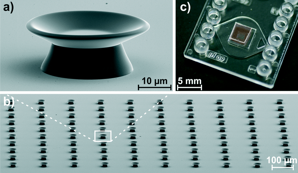 | ||
| Fig. 1 PMMA microgoblet lasers fabricated on a polysulfone substrate: (a) zoom-in of a single PMMA microgoblet laser supported on a polymer pedestal made from lift-off resist. (b) Array of 100 microgoblet lasers fabricated by parallel solution-based processing. (c) Photograph of a sensing chip: an array of 100 microgoblet lasers identical to Fig. 1b is integrated into a microfluidic chip. Transparency of the chip enables optical addressing of individual microgoblets through the lid via free-space optics. | ||
Optical probing and read-out
To bypass the challenge of probing the resonators via evanescent fibre coupling, we dope them with dye molecules and operate them as lasers.24 Active sensor cavities present an attractive alternative to their passive counterparts due to reduced linewidth of laser emission in comparison to the resonance linewidth of passive resonators.25 Moreover, such laser cavities can be efficiently probed and read out using free-space optics, thereby significantly facilitating sample alignment and integration into microfluidic structures.To minimize the costs and size of the optical pump unit, a laser diode is used for excitation. Pumping of WGM lasers with laser diodes has so far only been demonstrated using organic semiconductor thin-films as gain medium.26 However, due to photo-oxidation of the gain medium, these lasers could only be operated in a vacuum chamber, preventing actual sensing applications in a LoC. Here, we instead use the organic dye pyrromethene 597 (PM597) as gain material, which has been demonstrated as an efficient light emitter in various types of microlasers.27,28 The superior photostability of PM597 enables stable laser operation under common ambient conditions. The dye's absorption maximum lies in the green spectral range, while its emission occurs at orange-red wavelengths. Until recent years, laser diodes with direct emission in the green spectral range were not commercially available and pumping at these wavelengths could only be achieved with frequency-doubled solid-state lasers. Recent progress in the GaN-based laser diode fabrication has enabled devices with direct green emission. In our experiment, the beam of a green laser diode is loosely focussed onto the cavity and emission from the microgoblet laser is collected with a microscope objective from the top of the sample. Spectral analysis is performed with a Czerny–Turner spectrometer.
Microgoblet laser fabrication
Microgoblet lasers are fabricated on polymer substrates via spin-coating of the pedestal and resonator layers, mask-based optical lithography, and subsequent wet chemical etching of the pedestals. Finally, a thermal reflow step using a temperature above the glass transition point of PMMA is applied to smooth fabrication-induced defects along the cavity perimeter. This step additionally transforms the resonator disks into their characteristic microgoblet shape.Suitable substrate materials have to provide a high heat deflection temperature to maintain mechanical stability during the reflow process. The polymer polysulfone (PSU) is well suited for this purpose due to its high glass transition temperature of 190 °C, which is well above the reflow temperature used to anneal the PMMA resonators. PSU was purchased as 380 μm thick foils (LITE U, LITE GmbH) and further flattened via hot embossing between two silicon wafers to reduce its surface roughness. Flattened foils are approx. 350 μm thick and can easily be cut using a wafer dicing saw or common paper scissors.
The sacrificial layer between resonator and substrate has to allow for selective and isotropic etching without damaging the PMMA resonators or polymer substrates. Additionally, this material has to provide thermal stability during resonator reflow. Polydimethyl glutarimide-based lift-off resist (LOR) (LOR 30B, Microchem Corp.) provides all required properties as intermediate layer and allows selective wet chemical etching without dissolving the PMMA or the substrate.
A detailed schematic of the fabrication sequence is depicted in Fig. 2a–e. First, a five micrometre thick layer of LOR 30B is spin-coated onto the polymer foils as a spacer and subsequently baked on a hot plate for thermal annealing and to prevent pedestal deformation during resonator reflow. Resonators are structured from PMMA photoresist (PMMA 950k, MicroChem Corp.) mixed with the laser dye PM597 (Radiant Dyes Laser & Accessories GmbH) at a concentration of 2.56 × 10⁻⁵ mol g−1. The resist mixture is spin-coated onto the LOR layer and baked to remove residual solvent. PMMA disks with 50 μm diameter are structured via deep-UV lithography using a mask aligner (EVG 620, EV group). A 5′′ photomask containing multiple resonator arrays of 10 by 10 resonators was used for all exposures. In one single exposure, multiple resonator arrays on an area as large as a 4′′ wafer could be structured simultaneously. Exposed PMMA is subsequently developed in a 1![[thin space (1/6-em)]](https://www.rsc.org/images/entities/char_2009.gif) :1 mixture of methyl isobutyl ketone (MIBK) and isopropyl alcohol (IPA). Samples are immersed in a tetra-ethyl-ammonium-hydroxide-(TEAH)-based developer (101A Developer, Microchem Corp.) to underetch the PMMA disks isotropically. Etching is stopped at a pedestal diameter of approx. 25 μm, leaving the rim of the disks freestanding. To reduce fabrication-induced defects along the resonator rim, a thermal reflow is performed. Samples are heated on a hot plate to 130–135 °C under ambient atmosphere. At this temperature, softening of the PMMA allows thermal reflow of the disks due to the release of surface free energy. This induces the formation of the characteristic microgoblet shape. Finally, individual resonator arrays can be cut from the substrate using scissors. Integration of microgoblet laser arrays into microfluidic chips as depicted in Fig. 2f–h is described in detail below.
:1 mixture of methyl isobutyl ketone (MIBK) and isopropyl alcohol (IPA). Samples are immersed in a tetra-ethyl-ammonium-hydroxide-(TEAH)-based developer (101A Developer, Microchem Corp.) to underetch the PMMA disks isotropically. Etching is stopped at a pedestal diameter of approx. 25 μm, leaving the rim of the disks freestanding. To reduce fabrication-induced defects along the resonator rim, a thermal reflow is performed. Samples are heated on a hot plate to 130–135 °C under ambient atmosphere. At this temperature, softening of the PMMA allows thermal reflow of the disks due to the release of surface free energy. This induces the formation of the characteristic microgoblet shape. Finally, individual resonator arrays can be cut from the substrate using scissors. Integration of microgoblet laser arrays into microfluidic chips as depicted in Fig. 2f–h is described in detail below.
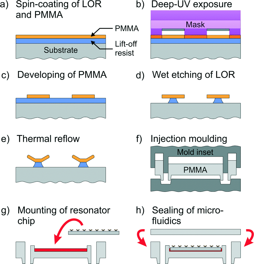 | ||
| Fig. 2 Fabrication scheme for all-polymer Lab-on-a-Chips depicted in cross-sectional view: (a) spin-coating of lift-off-resist (LOR) and dye-doped PMMA onto a polymer substrate, (b) structuring of resonator disks via deep-UV lithography, (c) developing of PMMA disks, (d) isotropic wet chemical etching of LOR to undercut the resonators, (e) thermal reflow on a hot plate to smooth the resonator surface and to transform the disks into the goblet shape. After dicing individual microresonator arrays from the substrate (not shown), single arrays are integrated into microfluidic chips: (f) replication of a microfluidic chip from PMMA using injection moulding, milling of depressions to support the resonator chips (not shown), (g) gluing of a diced resonator array into the microfluidic channel using UV curing adhesive, (h) sealing of the fluidic structures with a transparent polymer lid. | ||
Optical characterization
The optical performance of all-polymer microgoblet resonators is analysed by measuring quality factors of passive cavities and lasing thresholds of dye-doped cavities. In the transmission measurements performed to determine the quality factors, particular emphasis is put on investigating the differences between resonators structured by mask-based deep-UV lithography and electron beam lithography.Quality factor measurements
For quality factor measurements of the passive cavities, light of a tunable external cavity diode laser (Newport, New Focus Velocity TLB-6704) emitting around 635 nm was coupled to the microgoblet cavities by evanescent field coupling using a tapered optical fibre. Transmission through the fibre coupler was recorded with a photo diode synchronized to the swept laser source. Quality factors were estimated by the ratio of resonance wavelength to the full-width-at-half-maximum of the resonance dip. The measurements were carried out in the undercoupled regime to minimize influence of the tapered fibre on the quality factor. As the coupling parameter K, which is specified as the ratio of the resonator-fibre coupling rate and the intrinsic cavity loss rate, never exceeded 0.1 in our experiments, the measured loaded quality factor is comparable to the intrinsic quality factor, allowing direct comparison of the loaded quality factors of different resonators.29 Microgoblet resonators were structured by both electron beam lithography and deep-UV lithography. To provide sufficient thermal and electrical conductivity during electron beam exposure, only silicon substrates were used for samples prepared via electron beam lithography. Quality factor measurements were performed on multiple resonators of each sample type and highest measured values for the various types are shown in Table 1.| Quality factor | |
|---|---|
| Electron beam lithography (silicon substrate) | 1.5 × 10⁵ |
| Deep-UV lithography (silicon substrate) | 2.5 × 10⁵ |
| Deep-UV lithography (polysulfone substrate) | 1.4 × 10⁵ |
The quality factors of resonators structured by electron beam lithography and deep-UV lithography lie within the same order of magnitude. Furthermore, the quality factors of resonators fabricated on silicon and polysulfone substrates fall within the same range. Hence, the achievable quality factors are independent from the lithography technique and the substrate material.
Lasing thresholds
The absorption properties of PM597 incorporated into PMMA thin films were measured by absorption spectroscopy. To efficiently excite the dye close to its absorption maximum at 525 nm, a green laser diode (NDG7475, Nichia Corp.) emitting around 517 nm was used for optical pumping. The laser diode was operated with a diode driver (PicoLAS GmbH) in pulsed operation mode, emitting pulses of 20 ns FWHM pulse duration at a pulse repetition rate of 20 Hz. The emitted pulse energies were controlled by adjusting the diode current. For a maximum current of 2 A, the laser diode emitted 95 nJ per pulse. Light emitted from the laser diode was loosely focussed onto a single microgoblet laser under an angle of approx. 45°. Emission from the microgoblets was collected with a 50× microscope objective (NA = 0.42) from the top of the substrate. The collected light was analysed with a Czerny–Turner spectrograph with 500 mm focal length equipped with a 1200 mm−1 diffraction grating. As laser emission from microgoblet resonators occurs omnidirectional in azimuthal plane and is strongly confined in vertical direction, only a small fraction of light, which is scattered out of the horizontal plane, could actually be detected during this experiment.30To determine the lasing thresholds, emission spectra of the microgoblet lasers were recorded for increasing pump pulse energies. For each spectrum, the area under the investigated lasing peak was accumulated and plotted over the corresponding pump pulse energy. Linear fits were applied to the data points below and above the characteristic kink in the plot and the lasing threshold was determined by intersecting both lines. Fig. 3 shows an input–output curve of a microgoblet lasers structured by deep-UV lithography on a PSU substrate. The device has a lasing threshold of 0.54 nJ per pulse. Independent of the substrate material or the lithography technique used for device fabrication, lasing thresholds were typically below 1 nJ per pulse. Immersion of the devices in water resulted in an increase of the lasing threshold, which can be attributed to higher radiation loss in the cavity due to the decreased refractive index contrast. Still, lasing thresholds of immersed cavities typically stayed well below 3 nJ per pulse. Considering the maximum pulse energy emitted by the laser diode of 95 nJ, stable operation of the microgoblet lasers even significantly above their lasing threshold was possible.
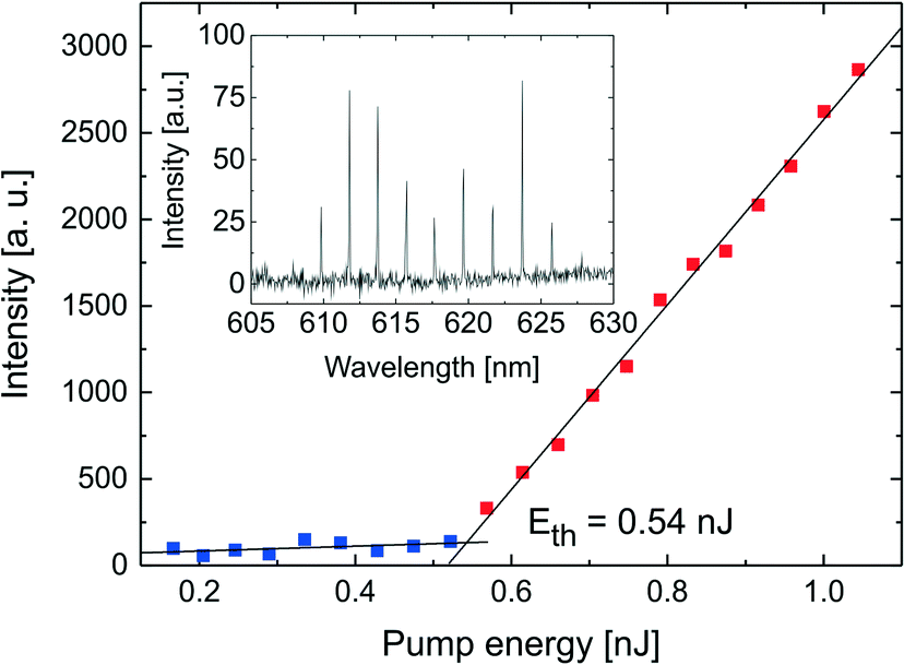 | ||
| Fig. 3 Input–output curve of a WGM microgoblet laser emitting at λ = 623.7 nm. The lasing threshold upon excitation with a green laser diode is 0.54 nJ in air. Data points below and above threshold are marked in blue and red, respectively. The inset shows a typical multimode emission spectrum of the investigated microgoblet laser when pumped well above the lasing threshold. | ||
On-chip integration and sensing
To experimentally demonstrate the applicability of the all-polymer microgoblet lasers in photonic LoC systems, resonator arrays were integrated into a state-of-the-art microfluidic chip. A schematic of the LoC and the optical and fluidic periphery is depicted in Fig. 4. The sensing capability of the integrated devices was validated by bulk refractive index sensing.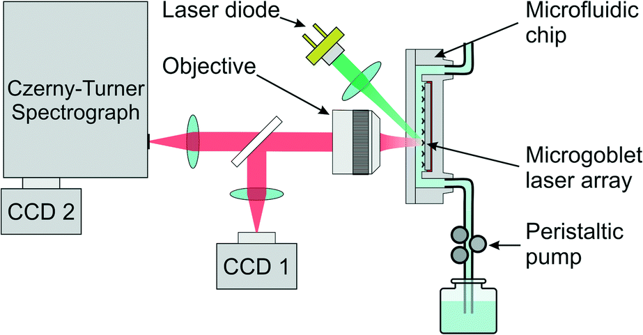 | ||
| Fig. 4 Schematic of the photonic LoC system: the all-polymer chip comprises an array of microgoblet lasers incorporated into a microfluidic channel. Individual microgoblet lasers can be optically pumped by focussing light emitted from a laser diode onto the chip. Positioning of the sample can be monitored with a camera (CCD 1). Emission from the microgoblet lasers is collected with a microscope objective and directed onto a grating-based spectrometer connected to a peltier-cooled detector (CCD 2). A peristaltic pump injects the analyte solutions from a reservoir into microfluidic channels on the chip. | ||
Integration into microfluidic chips
To facilitate fluidic handling and guide the analyte solutions to the microgoblet lasers, resonator substrates were incorporated into microfluidic channels. We used microfluidic chips provided by Microfluidic ChipShop GmbH (Jena, Germany) with dimensions of 75 by 26 mm2, matching the size of standard microscope slides. This format provides an easy-to-handle, standardized platform, which is compatible with commercial microscope systems.A schematic of the fabrication sequence for microfluidic chips is depicted in Fig. 2f–h. Microfluidic chips were replicated from PMMA via injection moulding. Subsequently, depressions with a depth of 400 μm were milled into the fluidic channels to support the resonator chips. The resonator substrates supporting an array of 100 microgoblet lasers were fixed inside these depressions using UV curing acrylated urethane medical adhesive. Finally, the microfluidic chips were sealed with a planar polymer lid. High transparency of the fluidic chips enables optical pumping and read-out of the microgoblet lasers through the lid. The fluidic periphery was connected to the microfluidic channels via mini Luer slips on the chip. A photograph of a microfluidic chip with an integrated microgoblet laser array is depicted in Fig. 1c.
On-chip refractometric sensing
Sensing with WGM resonators exploits spectral shifts of the cavity modes induced by a refractive index change in the periphery of the device. To experimentally verify the sensing capability of microgoblet lasers integrated into the microfluidic chips, the bulk refractive index sensitivity (BRIS) of the devices was determined. A series of five solutions with increasing refractive index was prepared by mixing deionized water with glycerol. For reference, the refractive index of each solution was measured with a refractometer (PAL-RI, Atago) prior to the experiment. The solutions were injected into the chip using a peristaltic pump at a flow rate of 350 μl min−1. The resulting spectral shifts of the lasing peaks were tracked with the spectrometer using a 2400 mm−1 grating for high spectral resolution. Prior to the measurement the resonators were immersed in deionized water for 15–30 min to eliminate any signal contributions due to swelling of the PMMA.31,32 Each measurement in high refractive index solution was followed by a referencing step in deionized water to induce a return of the mode to the starting wavelength. In order to track the center wavelengths of resonance peaks, the recorded spectra were fitted by a Gaussian model function. The recorded spectral shifts for solutions of refractive indexes from 1.3329 to 1.3355 are depicted in Fig. 5a. The resonance shifts upon injection of the high-index solutions are plotted in Fig. 5b. A bulk refractive index sensitivity of 10.56 nm per RIU was calculated from a linear fit applied to the data. The determined sensitivity is of the same order of magnitude as previously reported values for WGM resonators fabricated by surface-reflow.33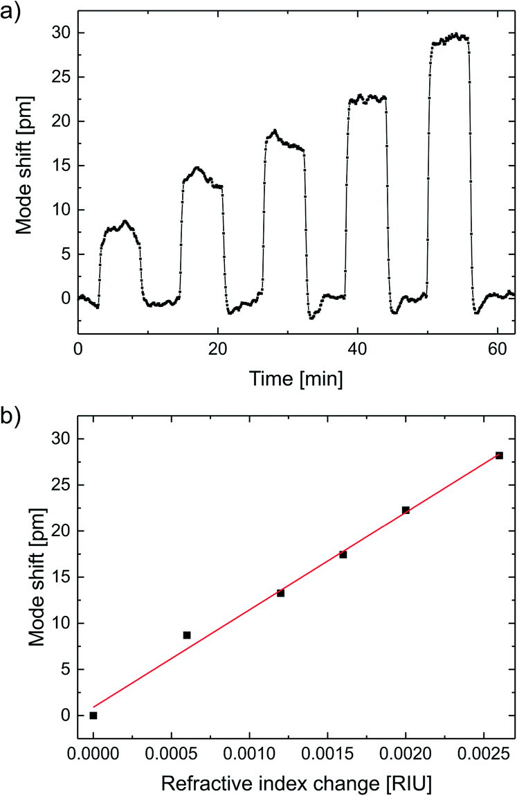 | ||
| Fig. 5 (a) Spectral shifts of a microgoblet laser mode upon injection of glycerol–water solutions with increasing refractive indexes of 1.3335 to 1.3355. Between subsequent injections of high-index solutions, deionized water with a refractive index of 1.3329 was injected for referencing. (b) A bulk refractive index sensitivity of 10.56 nm per RIU was calculated from the linear fit (red) applied to the data. | ||
Conclusion
We have demonstrated an all-polymer photonic sensing platform based on whispering-gallery mode microgoblet lasers integrated into microfluidic chips. Microgoblet lasers made from dye-doped PMMA have been fabricated as arrays of 100 cavities using a novel, fully parallel fabrication process. By supporting the resonators on pedestals made from lift-off resist, devices could be fabricated on low-cost PSU polymer foils via mask-based optical lithography, wet chemical etching and parallel thermal reflow. In contrast to silica-based microtoroid resonators, our fabrication technique replaces technically demanding vacuum-based dry etching and serial laser-induced reflow by solution-based processing and parallel thermal reflow. This concept can be scaled to large-area substrates and fabrication at significantly reduced device costs. Quality factors of fabricated microgoblet resonators exceeded 105. Microgoblet cavities doped with the laser dye pyrromethene 597 have been pumped efficiently using a compact and low-cost green laser diode for excitation. Lasing thresholds below 0.6 nJ per pulse have been recorded in air. Microgoblet laser arrays have subsequently been integrated into state-of-the-art microfluidic chips for easy fluidic addressing. In a proof-of-principle experiment we have demonstrated the functionality of the LoC via refractometric sensing with a bulk refractive index sensitivity of 10.56 nm per RIU.To the best of our knowledge, this is the first fully encapsulated lab-on-a-chip based on WGM resonators which are solely made from polymers and fabricated using parallel largely scalable fabrication processes. We believe that this concept will enable using the chips as low-cost disposables in a photonic sensing platform for point-of-care diagnostics. Handling and operation of our chips is significantly facilitated as no evanescent fibre coupling is required. Excitation and read-out of the resonators is solely achieved via free-space optics and hence allows for easy sample alignment.
In future work, the sensing chips may further be enhanced by integrating microoptical structures onto the polymer chip. Specifically, the read-out efficiency may be significantly increased by directing the microgoblet laser emission to the spectrometer using conical micromirrors.30 For specific sensing of multiple reagents, the surface of different resonators of the array may be functionalized via polymer-pen lithography (PPL) prior to on-chip integration.34 Multiplexed read-out of multiple microgoblet lasers may be used for referenced sensing or parallel label-free detection of different markers,35 which may allow, e.g., rapid screening in food safety assurance or identification of complex diseases. To enhance the portability of the read-out system, spectral analysis may be performed with a miniaturized spectrometer.36
Acknowledgements
The authors gratefully thank Andreas Bacher (IMT, KIT) for electron-beam lithography and Anika Hense (APH, KIT) for assistance with absorption measurements. U.B., S.K., T.S., T.W., and S.F.W. acknowledge financial support from the Karlsruhe School of Optics and Photonics (KSOP). S.K. acknowledges financial support from the Carl Zeiss foundation. This work was partly carried out with the support of the Karlsruhe Nano Micro Facility (KNMF, http://www.knmf.kit.edu), a Helmholtz Research Infrastructure at Karlsruhe Institute of Technology (KIT, http://www.kit.edu), and with the support of the Alfried Krupp von Bohlen und Halbach Foundation.References
- M. L. Kovarik, D. M. Ornoff, A. T. Melvin, N. C. Dobes, Y. Wang, A. J. Dickinson, P. C. Gach, P. K. Shah and N. L. Allbritton, Anal. Chem., 2013, 85, 451–472 CrossRef CAS PubMed.
- BCC Research LLC, Point of Care Diagnostics, Report HLC043D. Report: HLC043D, 49 Walnut Park, Building 2, Wellesley, MA 02481, USA, 2014 Search PubMed.
- B. Kuswandi, Nuriman, J. Huskens and W. Verboom, Anal. Chim. Acta, 2007, 601, 141–155 CrossRef CAS PubMed.
- F. B. Myers and L. P. Lee, Lab Chip, 2008, 8, 2015–2031 RSC.
- K. B. Mogensen and J. P. Kutter, Electrophoresis, 2009, 30, 92–100 CrossRef PubMed.
- M. C. Estevez, M. Alvarez and L. M. Lechuga, Laser Photonics Rev., 2012, 6, 463–487 CrossRef.
- W. Bogaerts, P. de Heyn, T. van Vaerenbergh, K. de Vos, S. Kumar Selvaraja, T. Claes, P. Dumon, P. Bienstman, D. van Thourhout and R. Baets, Laser Photonics Rev., 2012, 6, 47–73 CrossRef CAS.
- E. J. Smith, S. Schulze, S. Kiravittaya, Y. Mei, S. Sanchez and O. G. Schmidt, Nano Lett., 2011, 11, 4037–4042 CrossRef CAS PubMed.
- I. M. White, H. Oveys, X. Fan, T. L. Smith and J. Zhang, Appl. Phys. Lett., 2006, 89, 191106 CrossRef.
- T. Grossmann, M. Hauser, T. Beck, C. Gohn-Kreuz, M. Karl, H. Kalt, C. Vannahme and T. Mappes, Appl. Phys. Lett., 2010, 96, 013303 CrossRef.
- D. K. Armani, T. J. Kippenberg, S. M. Spillane and K. J. Vahala, Nature, 2003, 421, 925–928 CrossRef CAS PubMed.
- F. Vollmer, S. Arnold and D. Keng, Proc. Natl. Acad. Sci. U. S. A., 2008, 105, 20701–20704 CrossRef CAS PubMed.
- J. Zhu, S. K. Ozdemir, Y.-F. Xiao, L. Li, L. He, D.-R. Chen and L. Yang, Nat. Photonics, 2009, 4, 46–49 CrossRef.
- A. Ramachandran, S. Wang, J. Clarke, S. J. Ja, D. Goad, L. Wald, E. M. Flood, E. Knobbe, J. V. Hryniewicz, S. T. Chu, D. Gill, W. Chen, O. King and B. E. Little, Biosens. Bioelectron., 2008, 23, 939–944 CrossRef CAS PubMed.
- S. Arnold, R. Ramjit, D. Keng, V. Kolchenko and I. Teraoka, Faraday Discuss., 2008, 137, 65–83 RSC.
- M. D. Baaske, M. R. Foreman and F. Vollmer, Nat. Nanotechnol., 2014, 9, 933–939 CrossRef CAS PubMed.
- A. L. Washburn and R. C. Bailey, Analyst, 2011, 136, 227–236 RSC.
- F. Monifi, S. K. Ozdemir, J. Friedlein and L. Yang, IEEE Photonics Technol. Lett., 2013, 25, 1458–1461 CrossRef.
- P. Dumon, W. Bogaerts, V. Wiaux, J. Wouters, S. Beckx, J. van Campenhout, D. Taillaert, B. Luyssaert, P. Bienstman, D. van Thourhout and R. Baets, IEEE Photonics Technol. Lett., 2004, 16, 1328–1330 CrossRef.
- C.-Y. Chao and L. J. Guo, J. Vac. Sci. Technol., B, 2002, 20, 2862 CAS.
- P. B. Chu, J. T. Chen, R. Yeh, G. Lin, J. Huang, B. A. Warneke and S. J. Pister, in Solid State Sensors and Actuators, 1997, pp. 665–668 Search PubMed.
- J. C. Knight, G. Cheung, F. Jacques and T. A. Birks, Opt. Lett., 1997, 22, 1129 CrossRef CAS PubMed.
- X. Zhang and A. M. Armani, Opt. Express, 2013, 21, 23592–23603 CrossRef CAS PubMed.
- T. Grossmann, S. Schleede, M. Hauser, M. B. Christiansen, C. Vannahme, C. Eschenbaum, S. Klinkhammer, T. Beck, J. Fuchs, G. U. Nienhaus, U. Lemmer, A. Kristensen, T. Mappes and H. Kalt, Appl. Phys. Lett., 2010, 97, 063304 CrossRef.
- A. Schawlow and C. Townes, Phys. Rev., 1958, 112, 1940–1949 CrossRef CAS.
- S. Klinkhammer, T. Grossmann, K. Lull, M. Hauser, C. Vannahme, T. Mappes, H. Kalt and U. Lemmer, IEEE Photonics Technol. Lett., 2011, 23, 489–491 CrossRef CAS.
- Y. Yang, R. Goto, S. Omi, K. Yamashita, H. Watanabe, M. Miyazaki and Y. Oki, Opt. Express, 2010, 18, 22080–22089 CrossRef CAS PubMed.
- T. Wienhold, F. Breithaupt, C. Vannahme, M. B. Christiansen, W. Doerfler, A. Kristensen and T. Mappes, Lab Chip, 2012, 12, 3734–3739 RSC.
- P. E. Barclay, K. Srinivasan and O. Painter, Opt. Express, 2005, 13, 801 CrossRef CAS PubMed.
- T. Wienhold, S. Kraemmer, A. Bacher, H. Kalt, C. Koos, S. Koeber and T. Mappes, Opt. Express, 2015, 23, 1025 CrossRef PubMed.
- M. R. Foreman and F. Vollmer, Phys. Rev. Lett., 2015, 114, 118001 CrossRef PubMed.
- F. Stevens, J. Appl. Polym. Sci., 2005, 97, 1082–1089 CrossRef CAS.
- N. M. Hanumegowda, C. J. Stica, B. C. Patel, I. White and X. Fan, Appl. Phys. Lett., 2005, 87, 201107 CrossRef.
- U. Bog, F. Brinkmann, H. Kalt, C. Koos, T. Mappes, M. Hirtz, H. Fuchs and S. Köber, Small, 2014, 10, 3863–3868 CrossRef CAS PubMed.
- U. Bog, F. Brinkmann, S. F. Wondimu, T. Wienhold, S. Kraemmer, C. Koos, H. Kalt, M. Hirtz, H. Fuchs, S. Koeber and T. Mappes, Adv. Sci., 2015, 1500066 Search PubMed.
- G. Calafiore, A. Koshelev, S. Dhuey, A. Goltsov, P. Sasorov, S. Babin, V. Yankov, S. Cabrini and C. Peroz, Light: Sci. Appl., 2014, 3, e203 CrossRef CAS.
| This journal is © The Royal Society of Chemistry 2015 |