
 Open Access Article
 This Open Access Article is licensed under a Creative Commons Attribution-Non Commercial 3.0 Unported Licence
Development of an automated SILAR method for the sustainable fabrication of BiOI/TiO2 photoanodes†
Roberto Altieriab,
Fabian Schmitzab,
Manuel Schenkerab,
Felix Bollab,
Luca Rebecchic,
Pascal Schweitzerad,
Matteo Crisciab,
Ilka Kriegel c,
Bernd Smarslyab,
Derck Schlettweinad,
Francesco Lambertie,
Teresa Gatti*af and
Mengjiao Wang*f
c,
Bernd Smarslyab,
Derck Schlettweinad,
Francesco Lambertie,
Teresa Gatti*af and
Mengjiao Wang*f
aCenter for Materials Research, Justus Liebig University, Heinrich-Buff-Ring 17, 35392 Giessen, Germany. E-mail: teresa.gatti@polito.it
bInstitute of Physical Chemistry, Justus Liebig University, Heinrich-Buff-Ring 17, 35392 Giessen, Germany
cFunctional Nanosystems, Istituto Italiano di Tecnologia, via Morego 30, 16163 Genova, Italy
dInstitute of Applied Physics, Justus Liebig University, Heinrich-Buff-Ring 16, 35392 Giessen, Germany
eDepartment of Chemical Sciences, University of Padova, via Marzolo 1, 35131 Padova, Italy
fDepartment of Applied Science and Technology, Politecnico di Torino, Corso Duca degli Abruzzi 24, 10129 Torino, Italy. E-mail: mengjiao.wang@polito.it
First published on 5th September 2024
Abstract
BiOI is a promising material for use in photoelectrocatalytic water oxidation, renowned for its chemical inertness and safety in aqueous media. For device integration, BiOI must be fabricated into films. Considering future industrial applications, automated production is essential. However, current BiOI film production methods lack automation and efficiency. To address this, a continuous automated process is introduced in this study, named AutoDrop, for producing BiOI films. Autodrop results to be a fast and facile method for producing BiOI photoelectrodes. Nanostructured thin films of this layered material are prepared using a syringe pump to dispense the precursor solution onto a continuously spinning substrate. These films are integrated into a multilayered photoelectrode, featuring mesoporous TiO2 as an electron-transporting layer on top of FTO glass. In testing the photoelectrochemical performance of the BiOI/TiO2 photoelectrodes, the highest photocurrent (44 μA cm−2) is found for a heterojunction with a BiOI thickness of 320 nm. Additionally, a further protective TiO2 ultrathin layer in contact with BiOI, grown by atomic layer deposition, enhances the durability and efficiency of the photoanode, resulting in a more than two-fold improvement in photocurrent after 2 hours of continuous operation. This study advances the automation in the sustainable production of photoelectrode films and provides inspiration for further developments in the field.
1. Introduction
The use of semiconductor-based devices in photoelectrochemical (PEC) processes with a small carbon footprint offers a sustainable approach to address critical environmental challenges, particularly in hydrogen production through water splitting.1,2 PEC represents a promising technique that combines light absorption and electrocatalysis within a single device.3 However, photoelectrodes must be designed to overcome challenges such as chemical instability, electrolyte resistance, and mass transfer issues.4 The slow production at the laboratory scale and the difficulty in controlling the quality of photoactive material films significantly hinder their application and industrialization.5 Consequently, research efforts are needed to develop methods for producing photoactive materials with enhanced efficiency and improved quality control.Bismuth oxyhalides (BiOX, where X = Cl, Br, I) have garnered significant interest in photoelectrocatalysis due to their chemical stability under bias, favorable band gaps, and distinctive layered crystal structure, which provides a high surface area and potential active sites for catalytic reactions.6 They are based on bismuth, an a-toxic and non-critical element, which makes them even more appealing for technical applications.7 Among oxyhalides, BiOI exhibits the widest absorption in the visible light spectrum due to its small band gap, ranging from 1.8 eV to 2.3 eV, making it suitable for solar-driven photoelectrocatalytic applications.8 Based on its semiconducting character, BiOI encompasses its role in PEC water oxidation,9 dye degradation10 and the reduction of N2.11 However, applying BiOI in photoelectrocatalysis typically involves producing BiOI films by methods such as filtration,12 solvothermal,13 drop casting,14 electrodeposition,15 or chemical bath deposition.16 These techniques often result in films with inconsistent quality and performance and are not suitable for large-scale production and automation. Successive ionic layer adsorption and reaction (SILAR) is a low-cost, low energy consumption, and simple approach typically carried out by dip coating, where the substrate is rinsed in precursor solutions, with washing steps in between each cycle.17 However, achieving film homogeneity is challenging due to the multiple rinsing steps.18 To expedite the procedure and enhance reproducibility, BiOI thin films have been prepared using a spin coater (spin-SILAR).19 Instead of typical dipping cycles, controlling the amounts of precursor solutions becomes a key parameter in defining the thickness and quality of the films through spin-coating. However, further improvements are necessary to fully achieve automation in SILAR-like processes.
For integrating BiOI into PEC devices, it is important to improve the electronic properties of the material and adjust its processing. In previous work, pure BiOI has exhibited relatively low charge carrier mobility, hindering efficient transport of charge carriers and leading to a reduced PEC activity.20 Additionally, BiOI is prone to rapid recombination of photogenerated electron–hole pairs, further diminishing its efficiency in PEC processes.21 Therefore, BiOI is typically combined with other semiconductors to enhance charge transfer and mitigate recombination, with TiO2 being reported as a suitable component for improving its PEC properties.22–24 For instance, a BiOI/TiO2 heterostructure has been shown to be more photoactive than its individual components in the degradation of methyl orange.25 The formation of the heterojunction improves the transfer of photoinduced electrons from BiOI to TiO2, reducing charge recombination by forming a p–n junction. Combinations of BiOI and TiO2 nanorods or nanosheets have been reported for PEC water oxidation and organics degradation, demonstrating enhanced PEC activity of BiOI/TiO2 compared to just BiOI and thus showing the value of such binary heterojunctions based on a-toxic materials for future industrial applications.26–28
Apart from PEC efficiency, ensuring the stability of the photoelectrode is crucial. To enhance photoelectrode stability for water splitting, TiO2 and Al2O3 surface protection layers are commonly applied to prevent catalyst corrosion.29 Moehl et al. found that 30 nm amorphous TiO2 layers on top of fluorine-doped tin oxide (FTO) stabilize the photocurrent.30 By coating ZnO/Si photoelectrodes with an ultra-thin atomic layer deposited (ALD) TiO2, Kargar et al. significantly improved the stability from 60 to 100 minutes of continuous operation.31 Choi et al. have demonstrated that a thin layer of Al2O3 on Si can effectively prevent oxidation of Si and reduce the overpotential by providing surface passivation.32 Similarly, various studies have highlighted the benefits of applying TiO2 and Al2O3 protective layers on photoelectrodes like Cu2O, Si, Cu2ZnSnS4, and InP, showing that these layers serve as effective tools to enhance the operational stability of both photoanodes and photocathodes.33
Inspired by the recent advancements in BiOI film-production techniques and the verified PEC properties of BiOI/TiO2 heterojunctions, we present a modified spin-SILAR method, to render it less time-consuming and more automated. In this work, we propose the use of a syringe pump coupled with a spin coater to deliver Bi and I precursors with precise stoichiometry on substrates, as sketched in Fig. 1. This process, that we have named “Autodrop”, offers several advantages over standard SILAR and spin-SILAR methods. By continuously dropping the solutions onto the film instead of using discrete, repetitive cycles, this technique enhances the uniformity and consistency of the deposited layers while accelerating the overall process. Additionally, controlling the flow rates of the solutions allows for improved stoichiometry in the deposited films. Using this method, we produced BiOI thin films on mesoporous TiO2-coated FTO. The mesoporous TiO2 plays an important role in forming uniform BiOI layers and allows to build type-II heterojunctions. We systematically investigate the effect of film thickness on the band alignment and the performance of the resulting heterojunctions in PEC water oxidation. When BiOI has a thickness of 320 nm, the BiOI/TiO2 heterojunction shows an optimized photocurrent. Additionally, an ultra-thin TiO2 film deposited by atomic layer deposition (ALD) on top of the BiOI/TiO2 heterojunction further improves PEC properties and stability. This study demonstrates the potential for boosting automation in BiOI film production, achieving active layers of comparable quality to those produced manually but in significantly less time. Furthermore, it shows that detailed control over the band gap and thickness of the BiOI films can be achieved with such an automated process. The AutoDrop method has the potential to be further extended to the production of films of other materials typically synthesized via SILAR, advancing sustainable solution-processing towards greater automation and reproducibility.
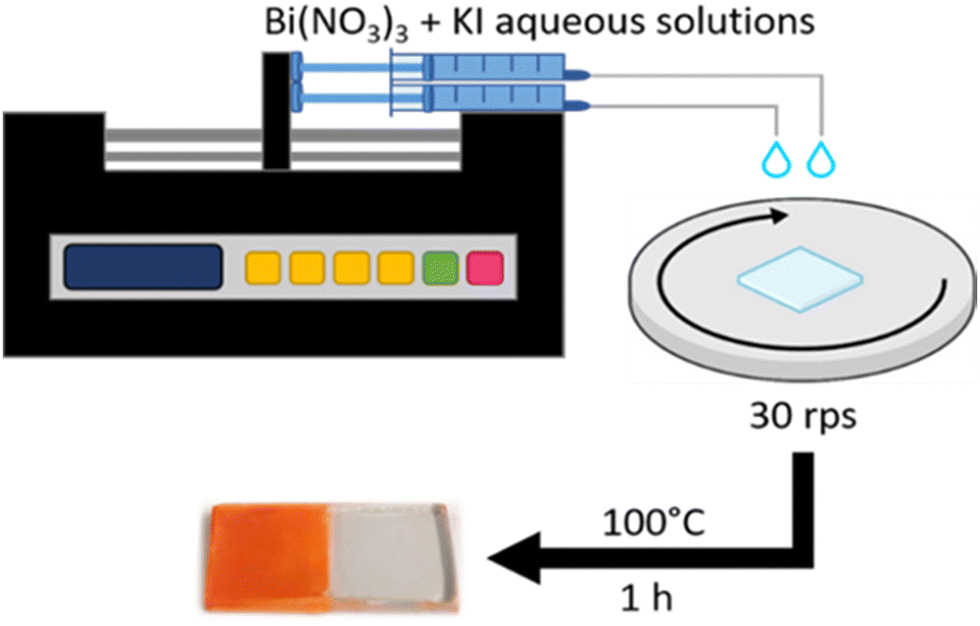 | ||
| Fig. 1 Schematic representation of the AutoDrop process developed in this work and used to produce BiOI thin films. | ||
2. Results and discussion
BiOI films were prepared either on pure FTO, FTO covered by a compact layer of TiO2 (FTO-planar TiO2), or FTO covered by a mesoporous layer of TiO2 (FTO-mesoporous TiO2) using the AutoDrop procedure to compare the uniformity of the achieved films (see Experimental section for practical details). As shown in Fig. 2, after applying the same amounts of precursors, the distribution of BiOI nanoflakes on bare FTO and mesoporous TiO2 substrates results in uniform films, while on planar TiO2, the BiOI film is less uniform, as observed in top-view scanning electron microscopy (SEM) images. Optical images of the three produced thin films also reveal a homogeneous color distribution across BiOI films on FTO and mesoporous TiO2 substrates. In contrast, the faded yellow color observed on planar TiO2 indicates a significant loss of precursor during the AutoDrop synthesis. This discrepancy in BiOI film quality is attributed to the different topologies of the substrates: as shown in Fig. S1 in the ESI,† FTO and mesoporous TiO2 feature larger grains and roughness compared to more planar compact TiO2, suggesting that a rough surface facilitates the nucleation of BiOI microplatelets during the continuous SILAR process.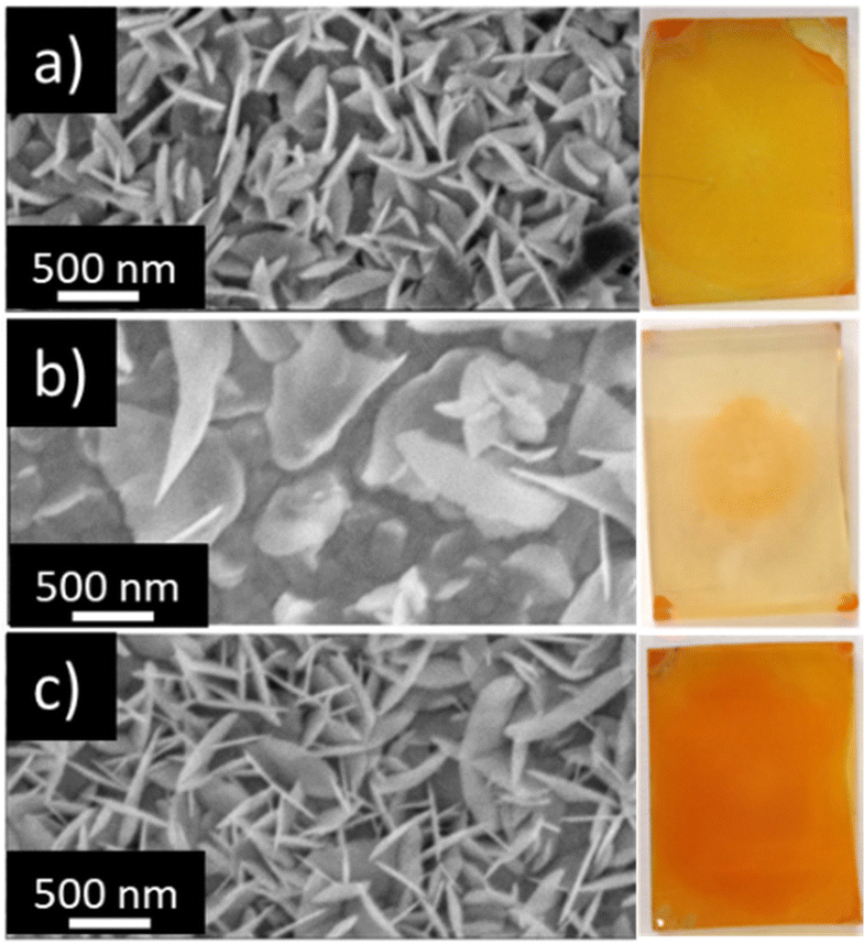 | ||
| Fig. 2 SEM images (left) and respective macroscopic photos (right) of large area BiOI thin films (1 × 2 cm2) prepared by the Autodrop method on top of (a) FTO glass, (b) FTO-planar TiO2, (c) FTO-mesoporous TiO2. | ||
In a further comparative study, a sample was prepared using a method similar to that employed by Putri et al., which involved manual spin-coating (spin-SILAR) of the precursors for up to 45 cycles (labelled as T/BiOI 45).19 As shown in Fig. S2 (ESI†), the film produced with the AutoDrop technique exhibits superior spatial uniformity. The continuous spinning and dropping process helps avoid border inhomogeneity, likely due to a reduced surface tension.34 Additionally, BiOI growth in the sample T/BiOI 1.2 (indicating the mesoporous BiOI/TiO2 heterojunction produced by deposition of 1.2 mL of precursors, vide infra) forms in 16 minutes with the AutoDrop method, whereas more than 30 minutes are needed to produce T/BiOI with 45 manual cycles. The diffuse reflectance spectra (DRS) indicate that the latter film has a similar absorbance to T/BiOI 1.2 (Fig. S2c, ESI†), suggesting that the samples produced with the AutoDrop method have similar optical properties to those produced with the traditional manual spin-SILAR.
The impact of varying amounts of BiOI on the mesoporous TiO2 substrates was investigated. Using the AutoDrop process, we adjusted the drop volume of precursor solutions while maintaining a constant injection rate of 75 μL min−1 to control the BiOI film thickness. The BiOI/TiO2 heterojunction films, with varying BiOI layer thicknesses, are labelled based on the drop volume of the KI solution used, with the volume of Bi(NO3)3 solution always equal to that of the KI solution, due to stoichiometric considerations. The samples are named as T/BiOI 0.4, T/BiOI 0.8, T/BiOI 1.2, and T/BiOI 1.6, corresponding to 0.4 mL, 0.8 mL, 1.2 mL, and 1.6 mL of the precursors, respectively, for the sake of clarity. The morphologies of the T/BiOI films for different BiOI precursor amounts (SEM top and side views) are shown in Fig. 3. All the BiOI films show a uniform distribution of BiOI vertical nanoflakes with different orientations on the microscale (Fig. 3a–d). The film prepared with the lowest BiOI precursor content (0.4 mL of KI and Bi(NO3)3, respectively) shows a less compact morphology compared to the other samples, as part of the mesoporous TiO2 is still visible in Fig. 3a in between the emerging BiOI nanoflakes. From the cross-sectional SEM images, shown in Fig. 3e–h, the analysis of the BiOI film thickness indicates an expected increase from ≈180 nm to ≈450 nm when the dropping volume increases from 0.4 mL to 1.6 mL.
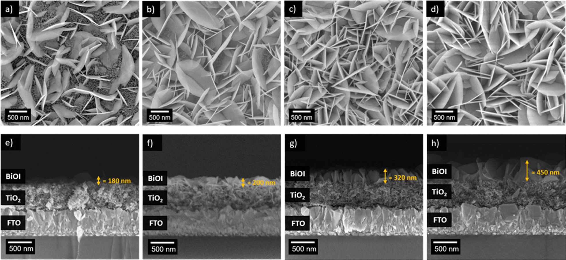 | ||
| Fig. 3 SEM images of T/BiOI films obtained by Autodrop with different dropping volumes in top-view and cross-section: (a) and (e) T/BiOI 0.4; (b) and (f) T/BiOI 0.8; (c) and (g) T/BiOI 1.2; (d) and (h) T/BiOI 1.6. | ||
By analysis of the relationship between the drop volume and film thickness, we hypothesize that KI and Bi(NO3)3 are first used to form BiOI nanoflakes with a dimension of around 200 nm until the substrate has no more space to host BiOI nanoflakes. When the drop volume of KI or Bi(NO3)3 reaches 0.8 mL, there is no space to form new BiOI nanoflakes, and the precursor solutions are applied to enlarge the size of the previously formed seed-flakes in a hierarchical fashion. The thickness growth rate is roughly 312.5 nm mL−1 after the drop volume exceeds 0.8 mL (Fig. S3, ESI†). Given that the dropping speed of both precursors is 75 μL min−1 and the general loss of precursor during spin-SILAR is approximately 95%, we estimate that the AutoDrop method forms about 8.26 BiOI atomic layers per minute (see ESI† for the calculations applied to estimate this number). Since the BiOI layers are randomly oriented on the substrate, the actual thickness of the BiOI layer is always greater than the theoretical thickness (Fig. S3b, ESI†).
The structure of the thin films was examined using grazing incidence X-ray diffraction (GIXRD) analysis. The diffractograms reveal the absence of any side phases, showing reflections solely from BiOI and TiO2 (Fig. 4a). Notably, T/BiOI 0.4 exhibits more intense TiO2 reflections compared to the other samples, suggesting greater exposure of TiO2 within T/BiOI 0.4. Additionally, the (001) signal of BiOI at ≈10° diminishes as the BiOI thickness increases. This decrease is likely due to the initial random orientation of BiOI nanoplates, which then tend to align vertically along the [001] direction on the TiO2 substrate, thereby decreasing the intensity of the (001) signal. It is also noteworthy to observe the relative changes in BiOI characteristic reflections at 29.6° and 31.7°, as shown in Fig. 4b. As the amount of BiOI increases, the intensity of the (110) signal becomes more pronounced compared to the (012) signal. This change can be attributed to a preferential growth along the (110) direction with the increasing amount of BiOI on the film. The XRD patterns obtained with different orientations of the samples corroborate this observation (see Fig. S4, ESI†). This vertical orientation of the flakes with respect to the FTO/TiO2 electron-selective contact is promising to improve charge extraction across the pnictogen oxyhalide layer.
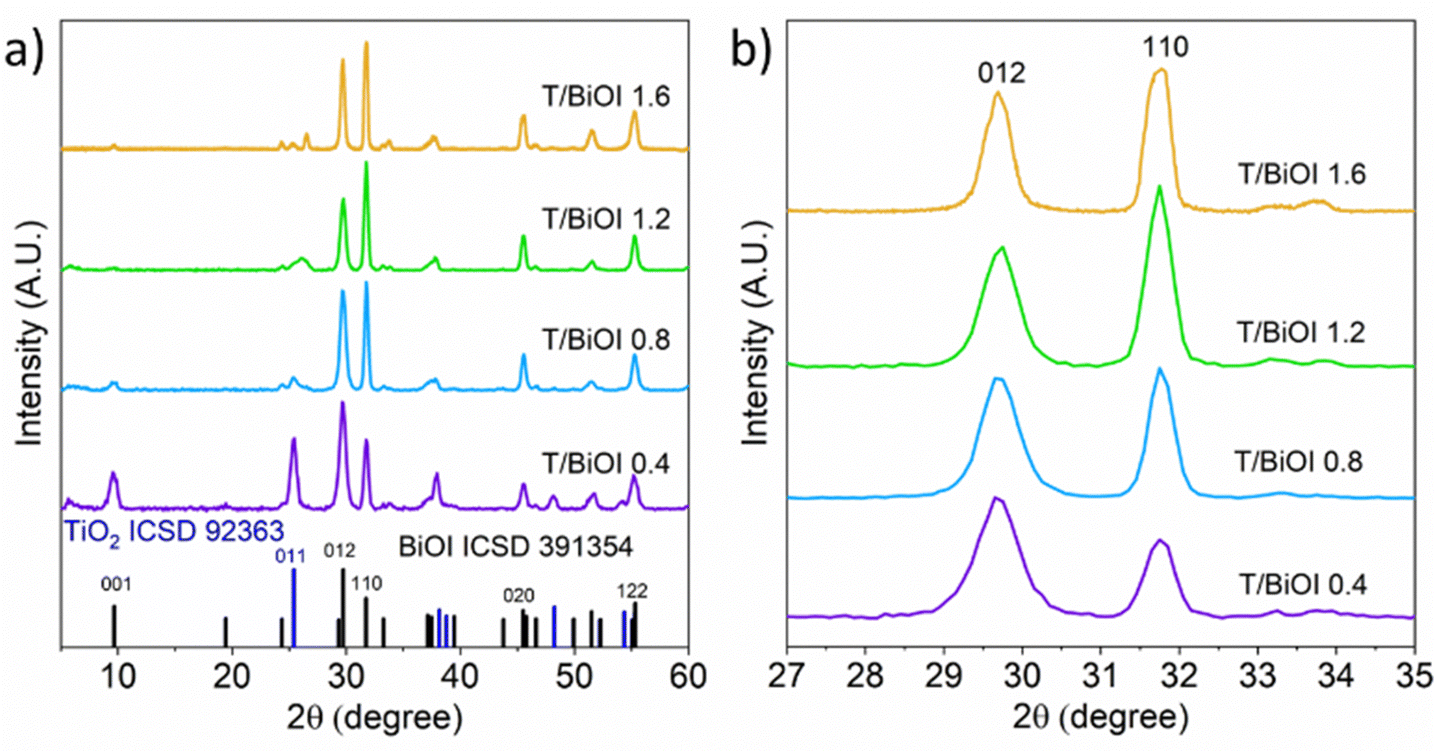 | ||
| Fig. 4 (a) GIXRD patterns of T/BiOI samples with references of anatase TiO2 and BiOI from the database; (b) magnification of (a) in the range of 27–35° highlighting the progressive increase in intensity of the (110) reflection in comparison with the (012) one. | ||
DRS analysis is illustrated in Fig. 5a. T/BiOI 0.4 exhibits absorption (here derived as a function of the measured reflectance obtained by applying the Kubelka–Munk transform) in the range of 300–550 nm. When the amount of BiOI is increased to 1.6 mL, the absorption range expands to 300–630 nm, and the overall absorption gradually intensifies. At a volume of 1.2 mL, the absorption reaches its peak, more than doubling compared to the T/BiOI 0.4 sample. However, further increasing the volume beyond 1.2 mL does not lead to additional improvement in absorption. The band-gap energy (Eg) was then calculated using the following eqn (1):
| αhν = A(νh − Eg)n/2 | (1) |
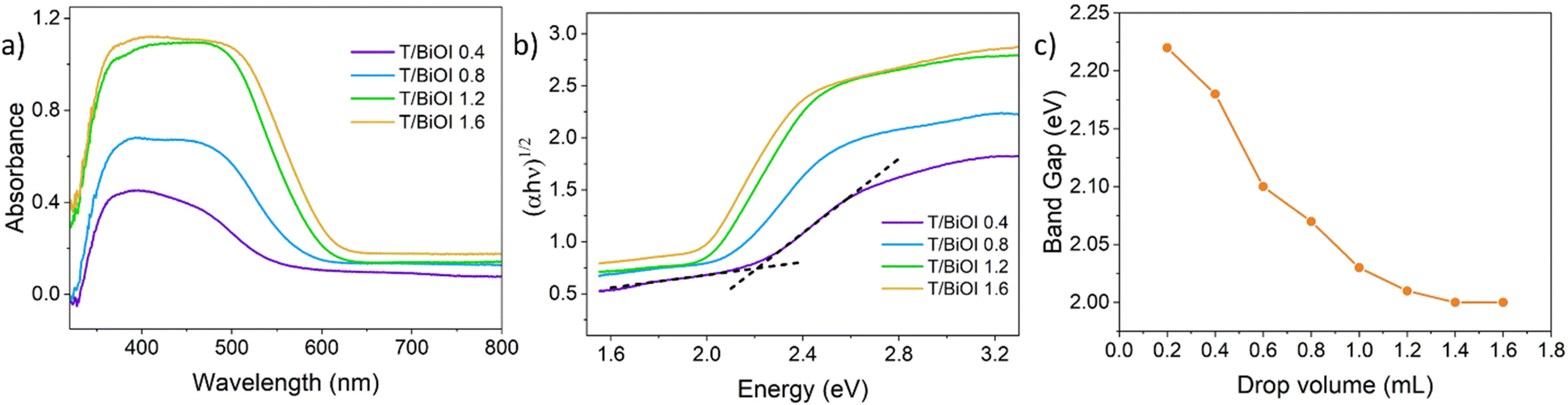 | ||
| Fig. 5 (a) UV−vis DRS and (b) Tauc plots of the T/BiOI samples prepared by Autodrop. (c) Relationship between T/BiOI films band-gaps and the drop volume of the precursor solutions. | ||
| Precursor volume (mL) | Eg (eV) |
|---|---|
| 0.4 | 2.18 |
| 0.8 | 2.07 |
| 1.2 | 2.01 |
| 1.6 | 2.00 |
The alignment of energy levels in the T/BiOI films was further characterized using a set of physical techniques. Fig. 6a and c show the contact potential difference (CPD) map of typical BiOI and TiO2 films obtained through Kelvin-probe force microscopy (KPFM) measurements. Since the work function (Wf) of the samples can be estimated from the fluctuation of CPD values, we find that the Wf values of BiOI and mesoporous TiO2 are 4.33 eV and 4.10 eV, respectively (Fig. 6b and d). XPS measurements in the range of the valence band maximum (VBM) also allows us to determine the difference between the Fermi level (EF) and the VBM in the two samples (Fig. 6e and f). The band gap was obtained from the Tauc plots (see Fig. 5b). With this information, we can draw the energy diagram for BiOI before and after contacting TiO2, as shown in Fig. 6h. The diagrams reveal a decrease in the Wf (and therefore an increase in EF) when BiOI is in contact with TiO2, indicating the formation of a type-II heterojunction in BiOI/TiO2. The higher conduction band minimum (CBM) of BiOI allows the injection of photogenerated electrons from BiOI to TiO2, while the photogenerated holes in TiO2 transfer and accumulate in BiOI to be exploited for further oxidation reactions. The band alignment of other T/BiOI samples were determined based on the Tauc plot in Fig. 5b, the Wf of BiOI in Fig. 6b, and the XPS spectra in Fig. S5 (ESI†). Although the AutoDrop process achieves fine-tuning of the band structure of the BiOI films, the band positions and band gaps of other T/BiOI samples still form type-II heterojunctions with TiO2 (Fig. 6i).
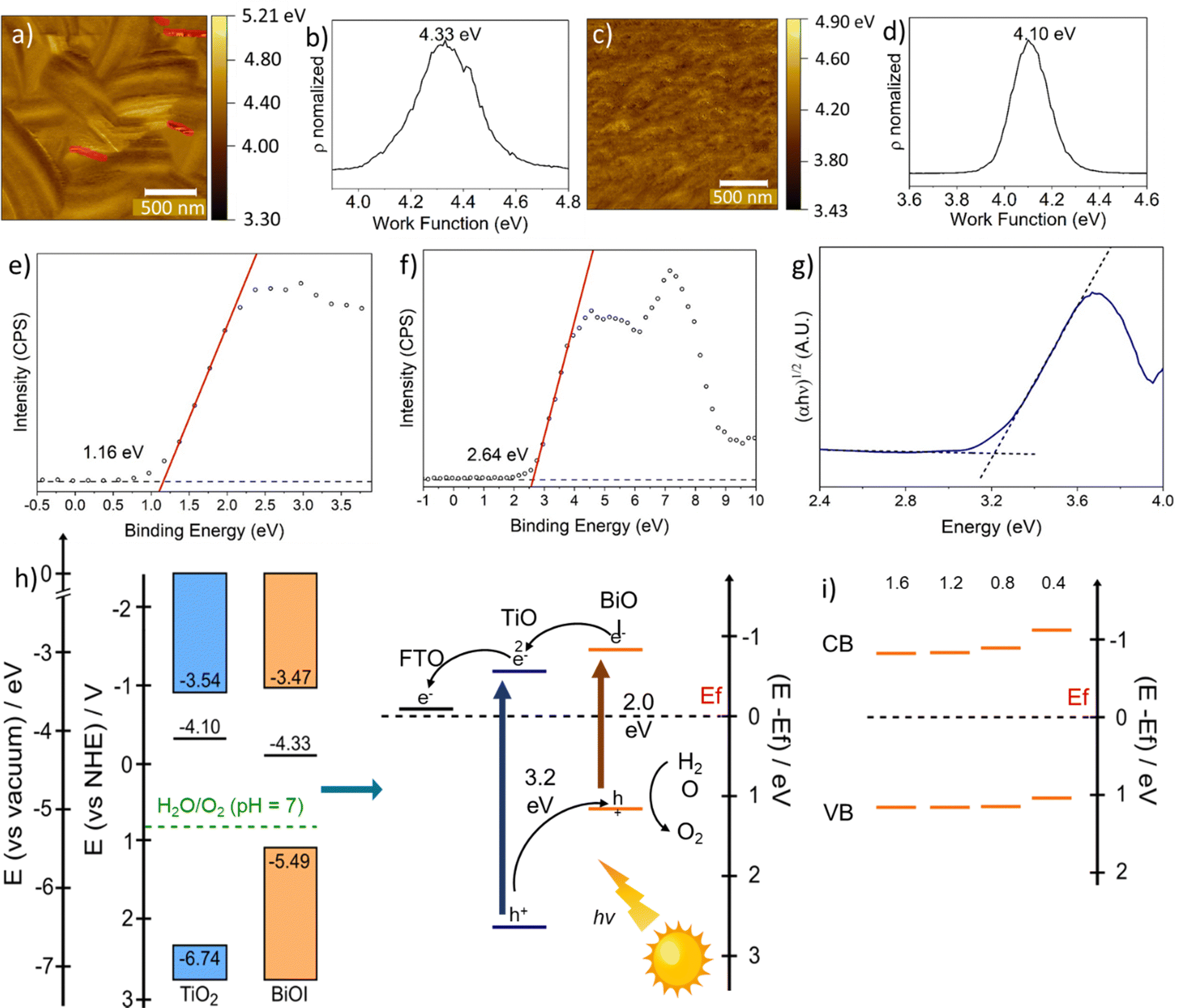 | ||
| Fig. 6 KPFM measurement image of (a) BiOI and (c) TiO2, respectively. Wf of (b) T/BiOI 1.2 (on top of mesoporous TiO2) and (d) mesoporous TiO2 thin films, respectively. In Fig. (b) only the marked regions were evaluated to avoid an influence of artifacts due to the steps across platelets. XPS spectra of (e) T/BiOI 1.2 and (f) mesoporous TiO2 in the region of the VBM. The binding energy scale is reported with respect to EF. The VBM occurs at the intersection of a line fit to the linear portion of the leading edge and the extended background line between the valence band maximum and EF. (g) Tauc plot of mesoporous TiO2 thin film on FTO. (h) Schematic diagram of energy level alignment, and the charge separation happening within the BiOI/TiO2 heterojunction under solar light illumination; (i) positions of band edges of BiOI films made with different drop volumes. Other XPS spectra are shown in Fig. S5 (ESI†) and Eg values in Fig. 4b and Table 1. | ||
Based on this detailed analysis, the position of the VBM of BiOI in the heterojunction lies in a region favourable for the oxygen evolution reaction (OER) (Fig. 6h). Thus, the PEC performance of the photoelectrodes was subsequently evaluated using a three-electrode system in a buffered phosphate solution at pH 7 under solar-simulated illumination. The linear sweep voltammetry (LSV) curves of all the T/BiOI samples are shown in Fig. 7a. All photoelectrodes displayed negligible dark current density from 0.2 to 1.8 V vs. the reversible hydrogen electrode (RHE). The photocurrent density of T/BiOI 0.4, T/BiOI 0.8, T/BiOI 1.2, and T/BiOI 1.6 was 26, 33, 44, and 38 μA cm−2 at 1.23 V versus RHE, respectively. The photocurrent density of the T/BiOI samples showed a significant increase compared to bare TiO2. The photocurrent of T/BiOI 1.2 was about twice as high as that of bare mesoporous TiO2. This enhancement in photocurrent can be attributed to the efficient separation and transfer of electrons and holes by the type-II heterojunction and large interface area between BiOI and TiO2, in addition to better harvesting of visible photons in this binary system. The decrease in photocurrent in T/BiOI 1.6 may be due to the BiOI layer being too thick and extending beyond the depletion region of the BiOI/TiO2 junction.24 The LSV comparison of T/BiOI 45 with T/BiOI 1.2 in Fig. S6 (ESI†) demonstrates the superior performance of T/BiOI 1.2, indicating that the AutoDrop method yields higher-quality films, resulting in better PEC performance. This enhancement is likely due to the closer connection between the TiO2 layer and the BiOI film produced by AutoDrop, compared to the BiOI film created using the traditional SILAR method.
 | ||
| Fig. 7 (a) LSVs, (b) transient photocurrent curves, (c) OCP decay profiles, and (d) EIS plots and the equivalent circuit for the fitting of the different T/BiOI photoanodes prepared by Autodrop and of bare TiO2, for the sake of comparison. | ||
The transient photocurrent curves of the photoelectrodes were evaluated at 1.23 V vs. RHE under chopped light to assess the photo-response and charge recombination behaviour of the photoelectrodes (Fig. 7b). The photocurrent of the T/BiOI samples is larger than that of bare TiO2. The photocurrent response of the BiOI layers exhibits a nonlinear increase with a maximum photocurrent of ∼40 μA cm−2, which is comparable to the published BiOI/TiO2 heterojunction photoelectrocatalyst by impregnating−hydroxylation method.28 Under simulated solar irradiation, all samples displayed sharp drops in photocurrent, indicating charge recombination or charge diffusion.37 The light-chopped open circuit voltage transients for T/BiOI photoelectrodes were measured under AM 1.5G illumination, as shown in Fig. 7c. Under illumination, the generation of charge carriers resembles a photovoltage. The signal shifting towards lower potentials is attributed to electron injection into the substrates. The open circuit photovoltage (OCP) is the difference between the open circuit voltage (Voc) under illumination and the Voc in dark. An increased OCP is observed when BiOI is deposited on TiO2, from 0.49 V to 0.65–0.80 V, indicating a higher concentration of surface electrons and better free charge production ability of the BiOI/TiO2 heterojunctions compared to bare TiO2.
The semicircular Nyquist plots obtained from electrochemical impedance spectroscopy (EIS) characterization of the photoelectrodes under illumination (Fig. 7d) indicate that electron transfer at the electrode/electrolyte interface plays a prominent role in the anodic process. The equivalent circuit in the inset of Fig. 7d can be used to analyse the reaction mechanisms involved in the electrode process, where Rs, Rct, and CPE represent the series resistance of the system, the charge transfer resistance, and the chemical capacitance, respectively.38,39 The Rct fitting results are shown in Table 2. The larger Rct value of TiO2 compared to all the T/BiOI samples indicates that the addition of BiOI layers improves the conductivity of the photoanodes. The Rct values of T/BiOI photoanodes initially decrease and then increase as the precursor volume increases. Among these, the T/BiOI 1.2 heterojunction exhibits the lowest Rct value of 10.1 kΩ, indicating the most efficient charge mobility and superior conductivity compared to other T/BiOI photoelectrodes, as expected for the best performing sample.40
| Sample | Rct (kΩ) |
|---|---|
| TiO2 | 99.6 |
| T/BiOI 0.4 | 37.3 |
| T/BiOI 0.8 | 35.8 |
| T/BiOI 1.2 | 10.1 |
| T/BiOI 1.6 | 29.4 |
The stability of the best BiOI/TiO2 heterojunction, namely T/BiOI 1.2, was evaluated in a PEC oxidation system through chronoamperometry measurements (Fig. 8a). The data reveal that the T/BiOI 1.2 photoelectrode's photocurrent decreases to 12 μA cm−2 after 120 minutes of continuous operation, comparable to the photocurrent of bare TiO2 (10 μA cm−2). This reduction in PEC performance may be due to the formation of an insulating hydroxide-based surface layer in aqueous media, as suggested by the work of Hahn N. T et al.41 To test this hypothesis, XPS analysis was performed on the T/BiOI 1.2 thin film before and after PEC testing (Fig. 8b and c). The O 1s XPS spectra show an increase in peaks at 531.3 and 532.3 eV, indicating an increase in –OH functionalities on the photoanode surface.
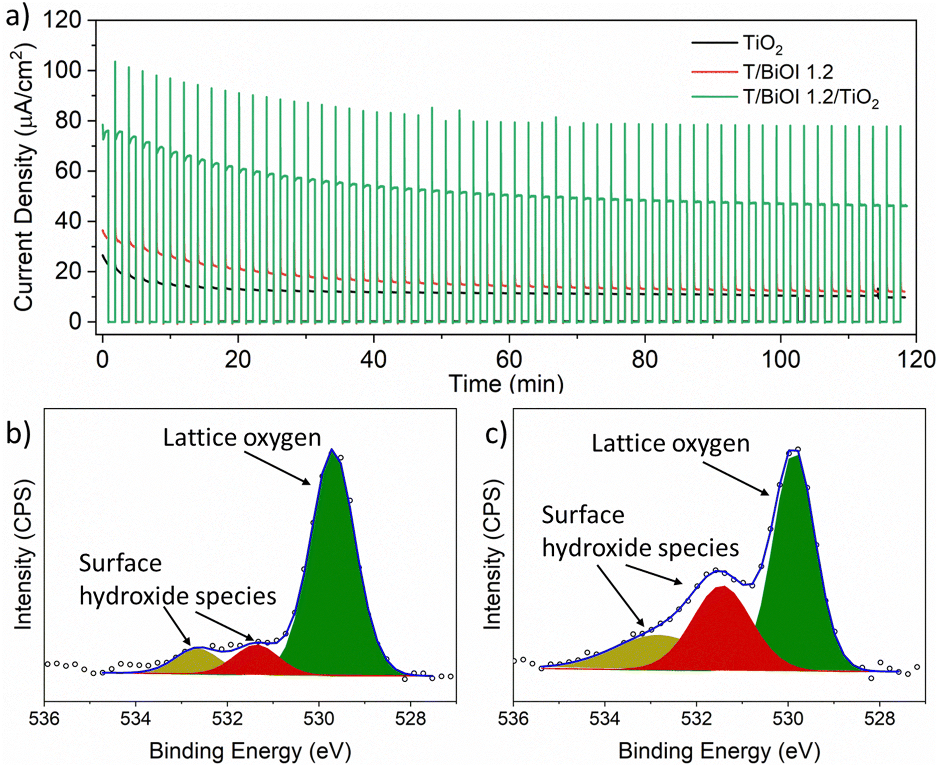 | ||
| Fig. 8 (a) Chronoamperometry at 1.23 V vs. RHE of the T/BiOI 1.2 film with and without a 20 nm ALD-TiO2 layer compared with a bare mesoporous TiO2 photoanode. High resolution XPS spectra of O 1s on T/BiOI 1.2 (b) before and (c) after the chronoamperometry measurement. | ||
TiO2 is a good n-type contact for photoactive heterojunctions, but is also widely used as a protective layer for various semiconductor photoelectrodes due to its high resistance to corrosion and decomposition.31 To enhance the PEC activity and stability of the T/BiOI 1.2 photoelectrode, a protective TiO2 layer was applied using ALD. ALD enables the creation of highly uniform and pinhole-free coatings, essential for effective passivation and protection.42 Kargar et al. demonstrated that a 20 nm TiO2 coating on a 3D ZnO/Si photoelectrode maintained PEC performance for over 24 hours under constant light and bias.43 Inspired by this work, we coated the T/BiOI 1.2 with a 20 nm TiO2 layer using ALD, creating the T/BiOI 1.2/TiO2 photoelectrode (lower thicknesses <20 nm were not successful in ensuring proper photoanode protection). The thickness value of ALD coatings can be easily determined by the number of cycles applied in the deposition set-up.44 Chronoamperometry at 1.23 V vs. RHE assesses the photocurrent stability over time (Fig. 8a). The ALD-TiO2 ultra-thin layer significantly improves the photocurrent density, reaching 46 μA cm−2 after 2 hours, nearly four times higher than the unprotected T/BiOI photoanode, confirming the necessity of a protective layer which acts as a tunnel barrier for BiOI in PEC applications, to enhance both activity and stability. Al2O3 is also frequently used as a protective layer in PEC water oxidation.45 To test whether an analogous Al2O3 ultra-thin layer could also enhance the PEC activity and stability of T/BiOI 1.2, a 20 nm Al2O3 protective coating was applied on T/BiOI 1.2 using ALD. Chronoamperometry results for T/BiOI 1.2/Al2O3 (Fig. S7, ESI†) show an initial photocurrent increase to approximately 70 μA cm−2, followed by a drop to less than 20 μA cm−2 after 60 minutes and further to 11 μA cm−2 after 120 minutes. Ultimately, the Al2O3 ultra-thin layer does not improve the performance compared to ultra-thin TiO2, suggesting that TiO2 endows better chemical and mechanical resistance to solution-processed nanostructured BiOI in the here employed aqueous electrolyte.46
Finally, the incident photon to current efficiency (IPCE) spectra for the T/BiOI 1.2 and T/BiOI 1.2/TiO2 photoanodes were measured at 1.23 V vs. RHE. Both T/BiOI 1.2 and T/BiOI 1.2/TiO2 showed a sharp increase in IPCE values for wavelengths below 420 nm, indicating efficient photocurrent generation from higher energy photons (Fig. S8, ESI†). Pure TiO2 performed poorly around 370 nm, but the junction with BiOI significantly increased the IPCE, highlighting enhanced charge separation. But pure TiO2 shows a higher IPCE at around 350 nm, which shows that the pure TiO2 has higher conversion efficiency under UV light, as TiO2 is a well-known photocatalyst under UV light.47 Furthermore, the photoelectric conversion efficiency of T/BiOI 1.2/TiO2 was approximately twice that of T/BiOI 1.2, demonstrating that the TiO2 protection layer effectively inhibits rapid charge recombination, enhancing performance in PEC water oxidation.
3. Conclusions
In summary, BiOI/TiO2 photoanodes were fabricated using an automated process derived from the SILAR method, integrating continuous delivery of two liquid solutions with spin-coating, which is here presented for the first time and named Autodrop. This approach enables the sustainable fabrication of thin films using aqueous-based inks at room temperature. Utilizing a syringe pump on a spin-coating platform, the Autodrop method offers precise control over the thickness and band gap of BiOI thin films grown on mesoporous TiO2 substrates by adjusting precursor volumes. This method enhances film homogeneity and production efficiency compared to manual techniques, underscoring its potential for scaling up solution-based processing of functional inorganic semiconductors.The Autodrop-produced BiOI/TiO2 heterojunctions were evaluated for their activity in OER, identifying an optimized photoanode produced with 1.2 mL of each precursor solution. To enhance stability, a protective ultra-thin TiO2 layer deposited via ALD was applied, resulting in improved photocurrent and durability of the photoanode during prolonged operation. This study provides valuable insights into automating SILAR-based thin films production, which holds great promise for future large-scale manufacturing of sustainable semiconductor-based photoelectrodes.
4. Experimental section
Materials
Bismuth(III) nitrate pentahydrate (Bi(NO3)3·5H2O) and potassium iodide (KI) were purchased from Thermo Fisher Scientific, the mesoporous titania precursor (Ti–Nanoxide T600/SC and Ti–Nanoxide BL/SC) was purchased from Solaronix and the FTO coated glass substrates were purchased from Sigma-Aldrich.Preparation of mesoporous TiO2 thin films
FTO-coated glass substrates were chosen as the supporting material. Initially, they underwent a thorough cleaning process in an ultrasonic bath, where they were sequentially immersed in deionized water and then in a 1![[thin space (1/6-em)]](https://www.rsc.org/images/entities/char_2009.gif) :1 mixture of acetone and isopropanol, each cycle lasting 15 minutes. Subsequently, the substrates were dried using compressed air and further treated with a UV-ozone cleaner (Ossila) for 15 minutes immediately prior to use. To fabricate mesoporous TiO2 films, a specific amount of Ti nanoxide T600/SC (Solaronix) was deposited onto the cleaned FTO glass substrate (30 μL per 1 cm2). The substrate was then rotated at 84 revolutions per second (rps) for 30 seconds. Following this, the substrate underwent calcination at 475 °C in an oven for 30 minutes, resulting in the formation of a mesoporous TiO2 film with an approximate thickness of 600 nm. Meanwhile, pure FTO glass substrates and FTO glasses with planar TiO2 were prepared as reference substrates for the subsequent deposition of BiOI. The deposition procedure for the planar blocking layer films mirrored that for mesoporous TiO2, except for the calcination step, where the films were heated at 550 °C for one hour.
:1 mixture of acetone and isopropanol, each cycle lasting 15 minutes. Subsequently, the substrates were dried using compressed air and further treated with a UV-ozone cleaner (Ossila) for 15 minutes immediately prior to use. To fabricate mesoporous TiO2 films, a specific amount of Ti nanoxide T600/SC (Solaronix) was deposited onto the cleaned FTO glass substrate (30 μL per 1 cm2). The substrate was then rotated at 84 revolutions per second (rps) for 30 seconds. Following this, the substrate underwent calcination at 475 °C in an oven for 30 minutes, resulting in the formation of a mesoporous TiO2 film with an approximate thickness of 600 nm. Meanwhile, pure FTO glass substrates and FTO glasses with planar TiO2 were prepared as reference substrates for the subsequent deposition of BiOI. The deposition procedure for the planar blocking layer films mirrored that for mesoporous TiO2, except for the calcination step, where the films were heated at 550 °C for one hour.
Synthesis of BiOI thin films
The precursor solutions used were 5 mM KI and 5 mM Bi(NO3)3·5H2O in aqueous form. It is crucial to freshly prepare the Bi(NO3)3 solution immediately before use because Bi(NO3)3 can undergo hydrolysis over time, forming insoluble basic salts like BiONO3, Bi2O2(OH)NO3, and Bi6O4(OH)4(NO3)6·H2O, which can affect the stoichiometry of the Bi precursor.48 The two solutions were simultaneously dispensed using a Harvard Apparatus-11 Plus 70-2212 Syringe Pump at a constant rate of 75 μL min−1 onto the substrate, which was continuously spinning at 30 rps on a KLM Spin-Coater SCV-10. After deposition, the substrates underwent a heating step at 100 °C for 1 hour to remove residual water. A schematic illustrating the preparation of BiOI layers on TiO2 thin films using the AutoDrop method is presented in Fig. 1. For comparison, a standard spin-SILAR method was used to prepare BiOI thin films by manually dropping 50 μL of each precursor solution, spinning for 20 seconds at 30 rps, and repeating this process for 45 cycles.Deposition of protection layers by ALD
The TiO2 protection layer was deposited using a PicoSun R200 ALD at a reaction temperature of 150 °C. Each cycle involved TiCl4 as the precursor (flow rate 100 sccm, pulse time 0.1 s, purge time 5 s), followed by water as the oxygen source (flow rate 150 sccm, pulse time 3 s, purge time 5 s). The growth rate was 0.06 nm per cycle, and a total of 333 cycles were performed to achieve a 20 nm thick TiO2 layer. Similarly, the Al2O3 protection layer was grown at the same reaction temperature of 150 °C. Each cycle utilized trimethylaluminum as the precursor (flow rate 100 sccm, pulse time 0.1 s, purge time 3 s), followed by water as the oxygen source (flow rate 150 sccm, pulse time 1 s, purge time 3 s). The growth rate was 0.106 nm per cycle, and 189 cycles were carried out to achieve a 20 nm thick Al2O3 layer.Characterization
SEM images were acquired using a Carl Zeiss GeminiSEM 560 field emission scanning electron microscope equipped with an InLens SE Detector. Imaging was conducted at an acceleration voltage of 3.00 kV, with a working distance of 3 mm, and a beam current of 100 pA. GIXRD measurements were performed on a PANalytical X’Pert PRO MRD instrument using Cu Kα radiation (λ = 1.5406 Å). The instrument operated at a current of 40 mA and an acceleration voltage of 40 kV. Optical absorption properties were characterized using a UV-vis-NIR Spectrometer (Agilent Cary 5000) with a scan resolution of 1 nm. Thin film absorption and transmission spectra were acquired using an integrating sphere (Diffuse Reflectance Accessory 150 mm, DRA-2500) attached to the spectrophotometer. Baseline acquisition was conducted with the empty integrating sphere. XPS analysis was carried out on a PHI 5000 VersaProbe II Scanning ESCA Microprobe (Physical Electronics) equipped with a monochromatized Al Kα X-ray source operating in high power mode (beam size 1300 μm × 100 μm, X-ray power: 100 W). Spectra were acquired with time steps of 50 ms, a step size of 0.2 eV, and an analyzer pass energy of 46.95 eV. Each detailed region averaged over 30 sweeps or a P/N ratio of 180. The sample surface was neutralized using slow electrons and argon ions, and the measurement was conducted under vacuum conditions ranging from 10−7 Pa to 10−6 Pa. Data analysis was performed using CasaXPS software. KPFM measurements were conducted with an AIST NT Vacuscope 1000 microscope operated below 5 × 10⁻⁶ mbar, using SPARK 350 Pt-coated AFM probes excited at around 300 kHz resonance frequency. The work function was determined by measuring the contact potential difference between the probe and sample via FM-KPFM, with an AC amplitude of 2 V at approximately 1 kHz. The probe work function was referenced against freshly cleaved highly oriented pyrolytic graphite (ZYB, MikroMasch) with a known work function of 4.6 eV, before and after each measurement.Photoelectrochemical characterization
For the PEC measurements, a SP-300 potentiostat/galvanostat from BioLogic, controlled by EC-Lab software, was utilized. The setup employed a three-electrode configuration comprising a platinum wire counter electrode, an Ag/AgCl (saturated KCl) reference electrode, and a working electrode. Potentials recorded against Ag/AgCl were converted to the RHE scale using the equation:| E (V vs. RHE) = E (V vs. Ag/AgCl) + 0.197 V + 0.059 V × pH |
The working electrode consisted of an FTO-coated glass substrate, with half of it masked by an adhesive strip to form the multilayer photoelectrode only on one side. The masked part with bare FTO was connected to a platinum plate electrode holder. The samples were illuminated from the front through a quartz window on the PEC cell with simulated solar light generated by an LS0106 Xenon arc lamp equipped with an LSZ189 AM 1.5G filter, adjusted to an intensity of 100 mW cm−2. EIS was conducted at 1.23 V vs. RHE under simulated solar light with the amplitude of 10 mV, sweeping frequencies from 100 kHz to 2 Hz.
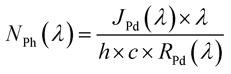
IPCE was calculated using an LSB5511000 W xenon short arc lamp from LOT-Oriel, coupled to an Acton SpectraPro 2300i monochromator. This measurement was performed concurrently with chronoamperometry under conditions identical to the PEC measurements. The IPCE at a specific wavelength (λ) was determined using the formula:

where JPd(λ) is the photocurrent density measured with the photodiode and RPd(λ) is the photodiode responsivity.
Data availability
The data supporting this article have been included as part of the ESI.†Conflicts of interest
There are no conflicts to declare.Acknowledgements
T. G. acknowledges the support of the European Research Council for the project JANUS BI (grant agreement no. [101041229]). M. W. and T. G. also thank Fondazione Compagnia di San Paolo for financial support through the “Bando TRAPEZIO - Paving the way to research excellence and talent attraction”. T. G. is also further grateful to Compagnia di San Paolo for the support through the Starting Grant ERC program. R. A., B. S. and T. G. would like to thank the DFG for project 460609161. F. B., M. C., I. K., B. S. and T. G. thank the European Commission for the project LIGHT CAP (grant agreement no. [101017821]).References
- J. Joy, J. Mathew and S. C. George, Int. J. Hydrogen Energy, 2018, 43, 4804–4817 CrossRef CAS.
- I. Roger, M. A. Shipman and M. D. Symes, Nat. Rev. Chem., 2017, 1, 1–13 CrossRef.
- M. Wang, M. Langer, R. Altieri, M. Crisci, S. Osella and T. Gatti, ACS Nano, 2024, 18, 9245–9284 CrossRef CAS PubMed.
- W. Yang, R. R. Prabhakar, J. Tan, S. D. Tilley and J. Moon, Chem. Soc. Rev., 2019, 48, 4979–5015 CAS.
- B. Moss, O. Babacan, A. Kafizas and A. Hankin, Adv. Energy Mater., 2021, 11, 2003286 CrossRef CAS.
- W. Li, X. Wang, Y. Zhang, S. Zhu, M. Zhao, H. Zhang, Y. Wang, D. Zhang, W. Ran, L. Zhang, N. Li, T. Yan, W. Li, X. Wang, Y. Zhang, S. Zhu, M. Zhao, H. Zhang, Y. Wang, D. Zhang, W. Ran, L. Zhang, N. Li and T. Yan, Adv. Mater. Interfaces, 2022, 9, 2200260 CAS.
- F. Schmitz, R. Bhatia, F. Lamberti, S. Meloni and T. Gatti, APL Energy, 2023, 1, 021502 CrossRef.
- A. A. Abuelwafa, R. M. Matiur, A. A. Putri and T. Soga, Opt. Mater., 2020, 109, 110413 CrossRef CAS.
- N. T. Hahn, S. Hoang, J. L. Self and C. B. Mullins, ACS Nano, 2012, 6, 7712–7722 CAS.
- X. Li, J. Xia, W. Zhu, J. Di, B. Wang, S. Yin, Z. Chen and H. Li, Colloids Surf., A, 2016, 511, 1–7 CrossRef CAS.
- Y. Bai, H. Bai, K. Qu, F. Wang, P. Guan, D. Xu, W. Fan and W. Shi, Chem. Eng. J., 2019, 362, 349–356 CrossRef CAS.
- B. Long, X. Liang, Y. Pei, X. Wu, X. Wang and M. K. Law, J. Mater. Sci. Technol., 2024, 198, 137–142 CrossRef.
- Y. Xin, Z. Wang, H. Yao, W. Liu, Y. Miao, Z. Zhang and D. Wu, Sens. Actuators, B, 2023, 393, 134285 CrossRef CAS.
- I. N. Reddy, B. Akkinepally, C. Bai and J. Shim, Crystals, 2022, 12, 1727 CrossRef CAS.
- J. Qiao, Y. Wang, S. Dong, Q. Liang and S. Shao, ACS Appl. Nano Mater., 2023, 6, 5664–5674 CrossRef CAS.
- M. Wang, A. Kafizas, S. Sathasivam, M. O. Blunt, B. Moss, S. Gonzalez-Carrero and C. J. Carmalt, Appl. Catal., B, 2023, 331, 122657 CrossRef CAS.
- S. P. Ratnayake, J. Ren, E. Colusso, M. Guglielmi, A. Martucci, E. Della Gaspera, S. P. Ratnayake, J. Ren, E. Della Gaspera, E. Colusso, M. Guglielmi and A. Martucci, Small, 2021, 17, 2101666 CrossRef CAS PubMed.
- J. Joo, D. Kim, D.-J. Yun, H. Jun, S.-W. Rhee, J. Sung Lee, K. Yong, S. Kim and S. Jeon, Nanotechnology, 2010, 21, 325604 CrossRef.
- A. A. Putri, A. A. Abuelwafa, S. Kato, N. Kishi and T. Soga, SN Appl. Sci., 2020, 2, 1–8 Search PubMed.
- H. Wang, Y. Liang, L. Liu, J. Hu, P. Wu and W. Cui, Appl. Catal., B, 2017, 208, 22–34 CAS.
- J. Di, J. Xia, M. Ji, L. Xu, S. Yin, Z. Chen and H. Li, J. Mater. Chem. A, 2016, 4, 5051–5061 RSC.
- B. Ogoh-Orch, P. Keating and A. Ivaturi, ACS Omega, 2023, 8, 43556–43572 CrossRef CAS PubMed.
- G. Pan, J. Li, G. Zhang, Y. Zhan and Y. Liu, J. Alloys Compd., 2023, 938, 168469 CrossRef CAS.
- X. Liao, T. T. Li, H. T. Ren, X. Zhang, B. Shen, J. H. Lin and C. W. Lou, Sci. Total Environ., 2022, 806, 150698 CrossRef CAS.
- X. Zhang, L. Zhang, T. Xie and D. Wang, J. Phys. Chem. C, 2009, 113, 7371–7378 CrossRef CAS.
- J. Liu, L. Ruan, S. B. Adeloju and Y. Wu, Dalton Trans., 2013, 43, 1706–1715 RSC.
- H. Chen, Y. P. Peng, T. Y. Chen, K. F. Chen, K. L. Chang, Z. Dang, G. N. Lu and H. He, Sci. Total Environ., 2018, 633, 1198–1205 CrossRef CAS PubMed.
- G. Dai, J. Yu and G. Liu, J. Phys. Chem. C, 2011, 115, 7339–7346 CrossRef CAS.
- J. Shi, X. Zhao and C. Li, Catal, 2023, 13, 217 CrossRef CAS.
- T. Moehl, J. Suh, L. Sévery, R. Wick-Joliat and S. D. Tilley, ACS Appl. Mater. Interfaces, 2017, 9, 43614–43622 CrossRef CAS PubMed.
- A. Kargar, K. Sun, Y. Jing, C. Choi, H. Jeong, G. Y. Jung, S. Jin and D. Wang, ACS Nano, 2013, 7, 9407–9415 CrossRef CAS.
- M. J. Choi, J. Y. Jung, M. J. Park, J. W. Song, J. H. Lee and J. H. Bang, J. Mater. Chem. A, 2014, 2, 2928–2933 RSC.
- R. Liu, Z. Zheng, J. Spurgeon and X. Yang, Energy Environ. Sci., 2014, 7, 2504–2517 RSC.
- Y. Gao, J. Zhang, Y. Su, H. Wang, X. X. Wang, L. P. Huang, M. Yu, S. Ramakrishna and Y. Z. Long, Mater. Horiz., 2021, 8, 426–446 RSC.
- X. Zhang and L. Zhang, J. Phys. Chem. C, 2010, 114, 18198–18206 CrossRef CAS.
- A. Crovetto, A. Hajijafarassar, O. Hansen, B. Seger, I. Chorkendorff and P. C. K. Vesborg, Chem. Mater., 2020, 32, 3385–3395 CrossRef CAS.
- L. Li, P. Dong Wu, W. Li, J. Huang, H. Li and S. Yang, Small Struct., 2024, 2300531 CrossRef CAS.
- X. Zhang, H. Yang, B. Zhang, Y. Shen and M. Wang, Adv. Mater. Interfaces, 2016, 3, 1500273 CrossRef.
- L. Yang, R. Wang, N. Zhou, L. Jiang, H. Liu, Q. He, C. Deng, D. Chu, M. Zhang and Z. Sun, Appl. Surf. Sci., 2022, 601, 154277 CrossRef CAS.
- T. Wang, L. Guo, H. Pei, S. Chen, R. Li, J. Zhang, T. Peng, T. X. Wang, L. L. Guo, H. Pei, S. T. Chen, R. J. Li, J. Zhang and T. Y. Peng, Small, 2021, 17, 2102957 CrossRef CAS PubMed.
- N. T. Hahn, S. Hoang, J. L. Self and C. B. Mullins, ACS Nano, 2012, 6, 7712–7722 CrossRef CAS.
- J. Zhang, Y. Li, K. Cao and R. Chen, Nanomanufacturing Metrol., 2022, 5, 191–208 CrossRef.
- A. Kargar, K. Sun, Y. Jing, C. Choi, H. Jeong, Y. Zhou, K. Madsen, P. Naughton, S. Jin, G. Y. Jung and D. Wang, Nano Lett., 2013, 13, 3017–3022 CrossRef CAS PubMed.
- M. Ylilammi, Thin Solid Films, 1996, 279, 124–130 CrossRef CAS.
- C. Liu, C. Zhang, G. Yin, T. Zhang, W. Wang, G. Ou, H. Jin and Z. Chen, ACS Appl. Mater. Interfaces, 2021, 13, 13301–13310 CrossRef CAS PubMed.
- V. Dias, H. Maciel, M. Fraga, A. O. Lobo, R. Pessoa and F. R. Marciano, Materials, 2019, 12, 682 CrossRef CAS PubMed.
- M. Wang, F. Zhang, X. Zhu, Z. Qi, B. Hong, J. Ding, J. Bao, S. Sun and C. Gao, Langmuir, 2015, 31, 1730–1736 CrossRef CAS PubMed.
- G. Gattow and D. Schott, Z. Anorg. Allg. Chem., 1963, 324, 31–47 CrossRef CAS.
Footnote |
| † Electronic supplementary information (ESI) available. See DOI: https://doi.org/10.1039/d4ya00405a |
| This journal is © The Royal Society of Chemistry 2024 |