
 Open Access Article
 This Open Access Article is licensed under a Creative Commons Attribution-Non Commercial 3.0 Unported Licence
Morphology-induced spectral modification of self-assembled WS2 pyramids†
Irina
Komen
 ,
Sabrya E.
van Heijst
,
Sonia
Conesa-Boj
and
L.
Kuipers
*
,
Sabrya E.
van Heijst
,
Sonia
Conesa-Boj
and
L.
Kuipers
*
Kavli Institute of Nanoscience, Department of Quantum Nanoscience, Delft University of Technology, The Netherlands. E-mail: L.Kuipers@tudelft.nl
First published on 30th September 2021
Abstract
Due to their intriguing optical properties, including stable and chiral excitons, two-dimensional transition metal dichalcogenides (2D-TMDs) hold the promise of applications in nanophotonics. Chemical vapor deposition (CVD) techniques offer a platform to fabricate and design nanostructures with diverse geometries. However, the more exotic the grown nanogeometry, the less is known about its optical response. WS2 nanostructures with geometries ranging from monolayers to hollow pyramids have been created. The hollow pyramids exhibit a strongly reduced photoluminescence with respect to horizontally layered tungsten disulphide, facilitating the study of their clear Raman signal in more detail. Excited resonantly, the hollow pyramids exhibit a great number of higher-order phononic resonances. In contrast to monolayers, the spectral features of the optical response of the pyramids are position dependent. Differences in peak intensity, peak ratio and spectral peak positions reveal local variations in the atomic arrangement of the hollow pyramid crater and sides. The position-dependent optical response of hollow WS2 pyramids is characterized and attributed to growth-induced nanogeometry. Thereby the first steps are taken towards producing tunable nanophotonic devices with applications ranging from opto-electronics to non-linear optics.
I. Introduction
Two-dimensional transition metal dichalcogenites (2D-TMDs) have recently attracted enormous scientific attention for their distinctive optical properties. Like graphene, TMD materials consist of layers held together only by van der Waals forces. 2D TMDs (e.g. MoS2, WS2, MoSe2, WSe2etc.) are atomically thin semiconductors, with a transition from indirect to direct bandgap in the few-layer limit.1 Due to their high binding energy, electron–hole pairs form stable excitons even at room-temperature. A pseudospin can be attributed to each of the two valleys 2D TMDs possess, making it possible to address them selectively with circularly polarized light.2–4 The electronic and optical properties of these 2D semiconductors, for instance the excitons and valley pseudospin, make them an interesting platform for opto-electronics5,6 and valleytronics7–9 applications.One of the ways of creating 2D TMD monolayer samples is by exfoliation from bulk.9 An alternative method to produce layered TMDs materials is Chemical Vapor Deposition (CVD).10–15 While CVD can reproduce horizontal layers as found in naturally occurring TMDs, adjusting the growth conditions enables the growth of nanostructures with exciting properties and applications in nanotechnology, for instance vertical walls, flowers and pyramids.16 Under certain CVD growth parameters TMDs materials form pyramid-like structures,17,18 having many active adsorption site useful for applications in hydrogen sensors19 and water disinfection,20 at the same time possessing interesting electronic properties like ferromagnetism21 and high mobility.22,23 Moreover, pyramid-like TMDs structures have applications in non-linear optics,22,24,25 as they exhibit higher non-linear optical conversion efficiency than monolayers due to the thickness increase, while demonstrating a much larger non-linear optical response than multilayer TMDs.
It is interesting to note that only in a limited number of studies in the literature photoluminescence of these spiral- or pyramid-like structures is reported.17,18,20,22 In some, the non linear optical response is studied.22,24,25 In most, the TMDs spirals and pyramids are studied using Raman spectroscopy.17–24 However, comparing the measured optical response of pyramid-like structures of different studies needs to be done with caution, as the terms spiral flake or pyramid are used for nanostructures that have different thicknesses, geometry and sizes.
Raman spectroscopy is a powerful tool to study 2D TMDs, as knowledge on the vibrational modes of the layers provides insights in their structure.26–28 Commonly studied are the characteristic vibrational modes of TMDs, the E12g that corresponds to the in-plane displacement of the atoms, and the A1g that corresponds to the out-of-plane displacement of the chalcogenide atoms, as well as the longitudinal acoustic phonon LA(M).27–30 Studying the Raman response as a function of temperature,31–35 excitation polarization27,29,36 and excitation wavelength,37–39 provides information on structural properties like number of layers, strain and defect density.
It is important to note that the existence of exciton resonances in 2D TMDs has large implications for its Raman response. Raman features are greatly enhanced when the excitation is in resonance with an excitonic transition.27,28,37–40 Resonance Raman spectroscopy on 2D TMDs materials results in the excitation of higher-order phononic resonances,41 which yields rich Raman spectra with many more modes than the two mentioned characteristic modes.
Many questions arise about the nature of the optical response from complex CVD-grown TMDs pyramid-like nanostructures. It is unknown how the nanogeometry of TMDs pyramids influences its photoluminescence and Raman response and how it depends on temperature and polarization. For potential applications, this knowledge is paramount.
Here, we study the Raman and photoluminescence response of CVD-grown hollow WS2 pyramids, comparing it to the optical response of WS2 monolayers. Even though the WS2 monolayers and pyramids are grown on the same substrate and under the same conditions, their measured optical response is completely different. We find, surprisingly, that the pyramids exhibit a strongly reduced photoluminescence (PL) with respect to horizontal layers. The reduced PL enables us to study the Raman signal of the hollow WS2 pyramids, that contains both the characteristic Raman peaks of flat layers and a great number of higher-order phononic resonances. In contrast with the monolayers, the measured optical response of the hollow WS2 pyramids is non-uniform over the nanostructures. Annular dark-field (ADF) scanning transmission electron microscopy (STEM) measurements confirm position-dependent variations in atomic arrangement.
II. Results and discussion
A. Hollow WS2 pyramids
Fig. 1a presents an SEM image of a CVD-grown hollow WS2 pyramid (the substrate is a SiN film on Si, see Methods). The WS2 is crystallized in a 3R-phase (see Fig. S2c, d and Section 1 in the ESI†). The clear lines along the pyramid sides indicate single steps (see Fig. S1c and S2a, b in the ESI†). The geometry of the darker middle becomes more clear when examining the AFM image in Fig. 1b. The height profile measured with the AFM along the blue line is presented in Fig. 1c. The bottom of the crater in the middle is roughly 5.6 nm high with respect to the substrate, whereas the pyramid sides reach a height of 44 nm. The inset of Fig. 1a displays a schematic representation of the hollow pyramid, depicting the stair-like sides in white and the crater with a bottom of finite thickness in the middle.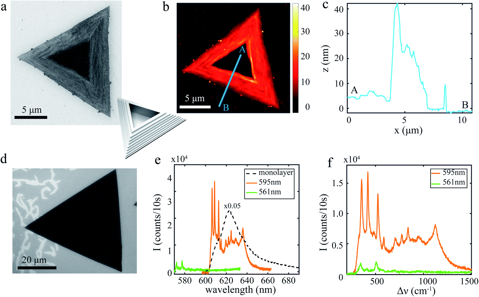 | ||
| Fig. 1 Hollow WS2 pyramids. (a) SEM image of the hollow WS2 pyramid. The lines along the sides indicate the single stair steps, whereas the darker region in the middle is the crater. (Inset) Schematic representation of the hollow pyramid. (b) AFM image of the hollow WS2 pyramid. The blue line indicates the position of the AFM crosscut depicted in (c), ranging from A the pyramid crater to B the substrate. (d) SEM image of a WS2 monolayer on the same substrate. (e) Photoluminescence spectrum of the WS2 monolayer (black dotted line), and spectra of a pyramid obtained with a 595 nm excitation (orange) and a 561 nm excitation (green). When converting the x-axis to wavenumber Δν in (f), the spectral response on the two different lasers overlaps nicely, indicating that the collected light originates from Raman processes rather than photoluminescence. | ||
Fig. 1e presents optical spectra obtained by exciting a WS2 pyramid at the stair-like side with either a 595 nm laser (orange) or a 561 nm laser (green). The spectra contain a similar sequence of peaks, but their spectral position does not overlap in wavelength. However, these peaks are located at the same relative frequency distance to the excitation laser, as depicted in Fig. 1f. The clear overlap of the larger peak positions in the spectra from the two different lasers indicates that the collected light originates from an inelastic Raman process rather than from photoluminescence.
Fig. 1d presents an SEM image of a single horizontal layer (monolayer) WS2 grown on the same substrate (next to hollow pyramids and monolayers, also fully grown pyramids are present on this substrate, see ESI, Fig. S1a, S5 and S6†). Comparing in Fig. 1e the optical response of the monolayer (black dotted line) with that of the pyramid, it becomes apparent that the pyramid exhibits a strongly reduced photoluminescence with respect to monolayer WS2. A small background under the Raman modes is visible in the spectrum of the pyramid around the PL wavelength of 630 nm. If this is remnant PL emerging from the hollow WS2 pyramid, it has an intensity of at most 1% of the WS2 monolayer (see ESI Fig. S3†). The immense reduction of the photoluminescence intensity from the hollow pyramids is unexpected. Even though the pyramid crater is only a few nanometers thin, the pyramid spectra do not resemble spectra of standard few-layered horizontal WS2 (see ESI Fig. S3f†). When the WS2 thickness increases from monolayer to bulk, it transitions from a direct to an indirect bandgap semiconductor.1 It is important to note that, in contrast to the hollow pyramids, the reduced PL from the direct bandgap can be easily measured for few-layered WS2.1,9 Moreover, the hollow WS2 pyramids do not exhibit any luminescence at the known wavelength of the indirect bandgap, as would have been expected from both bulk and few-layer WS2 (see ESI Fig. S3f†). Therefore we conclude that the increase of the layer number from monolayer WS2 to the pyramid crater cannot explain the reduction of the PL intensity. CVD-grown horizontal 2D TMDs flakes exhibit a similar amount of photoluminescence as exfoliated samples. Hence, the PL intensity reduction by at least two orders of magnitude of the hollow pyramids cannot merely be explained as being intrinsic to the CVD growth process, e.g. through an increase in defect density. Furthermore, the 3R-WS2 nanostructure cannot explain the PL intensity reductions, as 3R-WS2 exhibits the same photoluminescence as the naturally occurring 2H-WS2.42,43
We conclude that our hollow WS2 pyramids have a lower quantum efficiency than WS2 flakes: assuming that the optical absorption of a WS2 monolayer and a pyramid is the same, the quantum efficiency of these pyramids is at least two orders of magnitude lower than that of a monolayer WS2. Given the fact that the pyramids have a thickness of 5–44![[thin space (1/6-em)]](https://www.rsc.org/images/entities/char_2009.gif) nm, it is safe to assume that a pyramid actually absorbs more than a monolayer, therefore the quantum efficiency is likely to be at least another order of magnitude lower. We attribute the decrease in the quantum efficiency to the increase in possible non-radiative loss channels due to the presence of all the edges in the structure of these pyramids. The increase in non-radiative loss channels due to the edges in the pyramid structure is therefore the main factor that leads to a severe quenching of the exciton photoluminescence, without influencing the Raman modes.
nm, it is safe to assume that a pyramid actually absorbs more than a monolayer, therefore the quantum efficiency is likely to be at least another order of magnitude lower. We attribute the decrease in the quantum efficiency to the increase in possible non-radiative loss channels due to the presence of all the edges in the structure of these pyramids. The increase in non-radiative loss channels due to the edges in the pyramid structure is therefore the main factor that leads to a severe quenching of the exciton photoluminescence, without influencing the Raman modes.
The reduction of the PL enables us to study the Raman response of the hollow WS2 pyramids in more detail, as many Raman features are usually obscured by the PL spectrum. The pyramid spectra obtained with the 595 nm excitation exhibit roughly 10–12 Raman features, three of which have not been reported before for neither horizontal WS2 layers nor WS2 nanostructures (see Fig. 3). For the 561 nm excitation, fewer Raman features are visible in the spectra, and these features have a lower intensity. This can be attributed to the fact that the 595 nm excitation light is close to the A-exciton resonance, whereas the 561 nm is out-of-resonance with both the A- and B-excitons. Raman modes of TMDs can be greatly enhanced when they are excited in resonance with an excitonic transition.27,28,38–40
B. Structural characterization
In order to help interpret the studied optical response, we perform a detailed structural characterization of the hollow WS2 pyramids by means of Transmission Electron Microscopy measurements. Fig. 2 displays annular dark-field (ADF) scanning transmission electron microscopy (STEM) images taken in different regions of these WS2 nanostructures. Fig. 2a and b display atomic resolution ADF-STEM images of two different locations corresponding to the middle region of the hollow pyramid, while Fig. 2c corresponds to the pyramid side. By comparing these three images, we can clearly observe differences in the atomic arrangement. In Fig. 2a, the atomic distribution displays a well defined hexagonal shape, and this symmetry is highlighted by the corresponding fast Fourier transform (see inset in Fig. 2a). As we can observe from Fig. 2b, the atomic arrangements at this location are somewhat different from those observed in Fig. 2a. This structural variation is also reflected in the corresponding FFT (inset in Fig. 2b), where one of the Bragg reflections exhibits a reduced intensity (marked with a yellow circles to facilitate its visualization). Structural variation is also observed in the side region of the hollow pyramid. The difference in contrast in Fig. 2c corresponds to two stair-like steps in the pyramid side. By comparing their relative atomic arrangement, we can determine that, while the external step exhibits a clear hexagonal honeycomb structure, this arrangement is lost in the subsequent layer. Note also that, as observed from the results obtained in the middle region of the nanostructures, even across its sides the atomic arrangement can vary slightly (see also Fig. S7 in the ESI†). | ||
| Fig. 2 ADF-STEM of a hollow WS2 pyramid atomic resolution. Annular dark-field scanning transmission electron microscopy images taken in (a and b) the middle region, and (c). The side of a hollow WS2 pyramid. Subtle variations in the atomic arrangement can be observed. The corresponding FFTs, as given as insets in each of the panels, highlight this feature further. Changes in the Bragg reflections occur between them. One of which is a reduction of the intensity of one of the Bragg reflections in the middle region of the hollow pyramid, as marked by the yellow circles in (b). | ||
These subtle variations of the atomic arrangement might be induced by the local presence of strain, which in turn results into a slight change of the orientation of the flake. Importantly, the level of structural disorder is more marked in the middle of the pyramids as compared to the sides (see ESI Fig. S7†) due to the additional presence of free-standing WS2 flakes arising from the walls of the hollow pyramid.
C. Characterization of vibrational modes
In Fig. 3a we present a WS2 pyramid spectrum, acquired at the pyramid side, in which all Raman features are indicated with arrows. Commonly, only three Raman modes are measured on both horizontal TMDs layers or nanostructures. We measure 10–12 Raman features, three of which have not been reported previously (indicated in blue in Fig. 3a). The other modes can be attributed following a limited amount of previous investigations (see also Table 1). In order to analyze the spectra in more detail, we fit the overall spectrum with a collection of eleven Lorentzian lineshapes (red) and a background consisting of two Gaussians (grey) (see ESI† Section 1 for a discussion on the background). This way we are able to attribute the new Raman modes from hollow WS2 pyramids to being multiphonon resonances involving the LA(M) phonon, adopting the methodology for high frequency Raman features in MoS2.41 The blue line in Fig. 3b depicts the higher order resonances of A1g + n*LA(M). The peak 580 cm−1 is commonly attributed to A1g + LA(M),28,30–32 and the peak at 769 cm−1 is attributed to A1g + 2LA(M) by Molas et al.30 Thus we attribute the newly observed peak at 1128 cm−1 (n = 4) to A1g + 4LA(M). The red line in Fig. 3b depicts the higher order resonances of n*LA(M). The peak at 702 cm−1 is commonly attributed to 4LA(M),28,31 which is twice the first 2LA(M) Raman peak at 350 cm−1. Therefore we attribute the newly observed small shoulder of the last peak around 1057 cm−1 to 6LA(M). The expected resonance at 3LA(M) (red line in Fig. 3b) would spectrally overlap with the first silicon peak at 520 cm−1, as well as the expected resonance at n = 3 (blue line in Fig. 3b) would overlap with the second silicon peak 955 cm−1, so these possible features cannot be distinguished from the substrate response. The expected 5LA(M) (red line in Fig. 3b) would be around 880 cm−1, but is too dim to distinguish very clearly from the background. The peak at 833 cm−1 is 2*A1g, and the peak at 475 cm−1 is commonly attributed to LA(M) + 2ZA(M) (see Table 1). We conclude that the observed high-frequency Raman modes are multiphonon resonances involving the LA(M) phonon, excited because the 595nm laser is in resonance with the A-exciton.
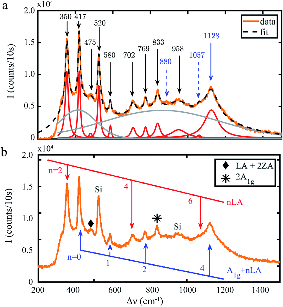 | ||
| Fig. 3 Characterization of Raman peaks. (a) The optical response of the hollow pyramids (orange) can be fitted by eleven Lorentzian lineshapes (red) and two Gaussians (grey). The Raman features are indicated by arrows with their spectral position in cm−1. The last three features (in blue) have not been reported before. (b) Part of the features can be explained as being multiphonon resonances involving the LA(M) phonon. The blue line depicts the higher order resonances of A1g + n*LA(M). The red line depicts the higher order resonances of n*LA(M). | ||
| Position | Std (cm−1) | Brightness | Attributed to | Possibly | Literature |
|---|---|---|---|---|---|
| 350 cm−1 | 1.6 | ++ | E12g/2LA(M) | 27–31, 38 and 44 | |
| 417 cm−1 | 1.5 | ++ | A1g | 27, 28, 30, 31, 38 and 44 | |
| 475 cm−1 | 4.7 | − − | LA + 2ZA or E′′(M) + TA(M) | 30 and 39 | |
| 520 cm−1 | 0.8 | ++ | Si | 3LA(M) | 45–47 |
| 580 cm−1 | 1.0 | +− | A1g + LA(M) | 28, 30–32,44 | |
| 702 cm−1 | 1.4 | + | 4LA(M) | 2E12g | 28,31,44, (30) |
| 769 cm−1 | 1.0 | + | A1g + E12g | A1g + 2LA(M) | 30 |
| 833 cm−1 | 1.2 | + | 2A1g | 30 | |
| 880 cm−1 | − − | 5LA(M) | |||
| 958 cm−1 | 3.3 | +− | Si | A1g + 3LA(M) | 45–47 |
| 1057 cm−1 | 1.0 | − − | 6LA(M) | ||
| 1128 cm−1 | 4.0 | + | A1g + 4LA(M) |
The highest frequency Raman modes have not been reported before on horizontal WS2 layers (indicated in blue in Fig. 3a). A possible explanation for not observing them on monolayers is that investigating Raman modes on horizontal WS2 layers is experimentally challenging because of the presence of photoluminescence, that is much brighter than any Raman feature. An intriguing alternative hypothesis is that the nanogeometry of the hollow pyramid plays a role in exciting the higher order Raman modes more resonantly, e.g. through a higher phonon density of states.
D. Position dependence of spectral features
The hollow WS2 pyramids contain two distinct regions: the crater in the middle and the stair-like sides. We find that these regions exhibit a different spectral response. This is in contrast from the more homogeneous spectral response for horizontal WS2 flakes (see ESI, Fig. S5 and S6†). Fig. 4a presents an intensity map of the first Raman peak (E2g, 2LA). To create this map, the maximum value of the fitted peak is used (see Fig. 3a). The peak intensity is higher and the peaks are more pronounced at the pyramid crater than at the stair-like sides. For the other WS2 Raman peaks, as well as at different temperatures and using different excitation wavelengths, this intensity distribution looks similar (see ESI Fig. S4†).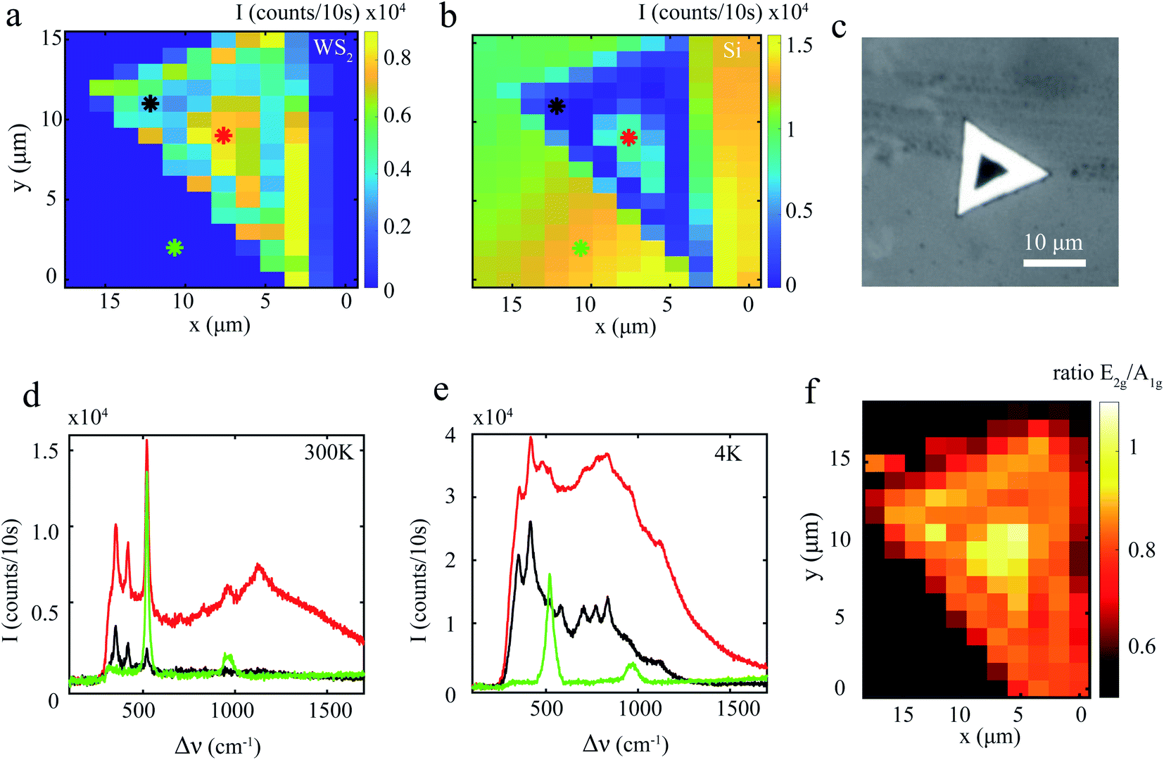 | ||
| Fig. 4 Position dependence of intensity and shape of spectra. (a) Intensity map of the first WS2 Raman feature around 350 cm−1, with a step size of around 1.5 μm. The stars indicate the positions of the spectra in (d and e). Note that the x and y axis in the map are slightly skewed due to experimental constraints (see Experimental section). (b) Intensity map of the Si Raman peak at 520 cm−1. (c) Optical image of a hollow WS2 pyramid. Note the white colour at the sides, indicating a clear increase in scattering from the sides with respect to the top. (d and e). Pyramid spectra at 300 K and 4 K. The substrate spectrum (green) shows the two Si peaks at 520 and 955 cm−1. The spectrum at the hollow part of the pyramid (red) has an overall higher intensity than at the side (black). (f). Map of the ratio between the first two Raman features in the spectra (E2g/A1g). | ||
Fig. 4b presents an intensity map for the silicon peak at 520 cm−1. As expected, there is a constant intensity for the substrate next to the pyramid. It is interesting to note that the intensity of this substrate peak also decreases on the pyramid edges. We hypothesise that light scatters a lot from the stair-like pyramid sides, as seen from the bright white colour of the sides in the optical image (Fig. 4c). This both reduces the available excitation light to excite Raman modes, and scattering of the resulting Raman response reduces the detected light, including the Raman response of the silicon substrate. Fig. 4d and e depict spectra on three different positions: on the hollow pyramid middle (red), on the substrate (green) and on the pyramid side (black) (indicated by stars in Fig. 4a and b). In both the room temperature spectra in Fig. 4d and 4 K spectra in Fig. 4e (temperature dependence will be discussed later), the two silicon peaks at 520 and 955 cm−1 can be clearly distinguished (in green). The spectrum at the pyramid crater (red) has clearly a higher overall intensity. In addition to the Raman peaks, there is also a background visible. Especially at 4 K, this background signal becomes extremely high, turning the signal from all the higher frequency Raman modes into mere shoulders. Based on its spectral position, we attribute this background to intermediate gap states or defect states (see ESI Fig. S3†). It is interesting to note that this background is significantly higher in the pyramid crater than on the sides, which might be originated by the presence of crystallographic defects.
Fig. 4f presents a map of the intensity ratio between the first two Raman peaks (E2g/A1g). Just like the intensity of the individual peaks, this intensity ratio is also non-uniform over the WS2 pyramid. In the pyramid crater, the peak ratio is approximately 1.0, whereas on the stair-like sides, the A1g peak is higher. The difference in peak ratio between the pyramid crater and sides is also present and much higher for the 561nm excitation (see ESI Fig. S5†). Note that the spectral features of a fully grown pyramid are very similar to the spectral response from the hollow pyramid sides (see ESI Fig. S5†). We conclude that both the peak intensity and the overall shape of the spectra are non-uniform along the WS2 pyramid, behaving differently at the hollow pyramid crater and the stair-like sides. This indicates a difference in the atomic arrangement between the two parts of the pyramid.
We also find a spatial non-uniformity in the spectral position of the peaks. Fig. 5a depicts the spectral position of the first WS2 Raman peak (E2g, 2LA) as a function of position. This spectral position is fairly uniform over most of the nanostructure, except for the right edge, where the spectral position is red shifted significantly up to 320 cm−1. Moreover, a small blue shift of the peak is seen on the left pyramid edge. The second WS2 Raman peak exhibits a similar spectral shift (not shown), as do spectra obtained for a 561 nm excitation. This spectral shift of peaks becomes more evident when comparing the spectra at the positions of the blue stars (Fig. 5b). The second line indicates the position of the silicon peak at 520 cm−1, which is clearly constant in all three spectra. However, when comparing the line at 355 cm−1 with the position of the first Raman peak, it is clear that the WS2 peaks in the spectrum are blue shifted.
 | ||
| Fig. 5 Position dependence of spectral position. (a) Map at 4 K of the spectral position of the first WS2 Raman feature (2LA(M), E2g), with a step size of around 1.5 μm. The spectral position is fairly homogeneous over most of the pyramid, except for the edge, where it is blue shifted up to 320 cm−1. The stars indicate the position of the spectra in (b). Three gray lines are drawn as guides to the eye. Comparing the position of the Si peak of the three spectra with the line at 520 cm−1 indicates that the spectral position of this peak does not shift. Comparing the position of the first WS2 peak with the line at 355 cm−1 does indicate the large shift of the spectrum on the pyramid edge (light blue) with respect to the rest of the nanostructure. | ||
The spectral position of Raman modes in TMD materials is known to depend on the number of layers.21,22,26–28 One might therefore have expected a gradual spectral shift along the stair-like sides of the pyramid, because of their gradual increase in WS2 layer thickness. Unfortunately, the diffraction-limited laser spot of size 450nm (see Methods) is much bigger than the width of the individual terraces. Therefore, if the size of the steps is one or even a few layers, we do not have the resolution to distinguish thickness-dependent changes in the Raman response of individual steps. The changes in the Raman response are smallest for low N, where N is the number of layers. The reported difference in spectral position for different layer thicknesses is at most 5 cm−1 (between a monolayer and a bilayer), much less than the shift of 30 cm−1 that we observe at the edge of this pyramid. Therefore this spectral shift cannot be explained by a thickness increase alone.
The spectral position of Raman modes in TMD materials does not only depend on the number of layers, it is also known to be influenced by the defect density,48,49 strain50,51 and pressure.33 The reported shift due to strain is 2–3 cm−150,51 and due to an increased defect density is 5–10 cm−1.48,49 For both strain and defects, the A1g peak is much less affected than the E2g peak. The reported shift due to pressure is up to 40 cm−1 for pressures up to 20 GPa.33 Since our measurements were performed in either ambient (room temperature) or vacuum (low temperature) conditions, we do not expect a spectral shift due to pressure. It is not unlikely that a large defect density and/or the presence of strain are present in the hollow pyramids. Interestingly, spectra taken on fully grown WS2 pyramids with curved edges do exhibit small shifts in the spectral peak position along the edges with highest curvature, where a higherstress or strain is expected (see ESI Fig. S6†). Therefore we assume that the origin of the large spectral shift in the hollow WS2 pyramid in Fig. 5 lies in a combination of the mentioned effects of defect density and strain or stress. Having said that, the previously reported shifts, even when added, are much lower than the 30 cm−1 that we observe on the edge of the hollow pyramid, so we cannot exclude unknown other causes related to the specific nanogeometry of the hollow pyramid.
In this context, it is interesting to note that we measure an average spectral position of the first Raman peak on a WS2 monolayer of 357 cm−1, which is higher than the average of 350 cm−1 of this and other WS2 pyramids (see ESI Fig. S6†). Given that the first WS2 Raman feature is a combination of the E2g and 2LA(M) phonon, we hypothesise that the first Raman feature in the monolayer has a larger contribution from the E2g than the same first feature in the hollow pyramid spectra.
We conclude that the spectral features of the hollow pyramids, namely intensity, peak ratio and spectral peak position, vary in space over the nanostructures. This in contrast with the homogeneous distributions of these spectral features on a WS2 monolayer. Moreover, the spectral position of the first WS2 Raman feature is different for a WS2 monolayer than for a hollow WS2 pyramid, indicating a larger contribution from the E2g than the 2LA(M) phonon.
E. Temperature dependence of spectral features
Studying the temperature dependence of spectral features provides insights on the structural properties of the WS2 pyramids. Fig. 6a presents spectra at four temperatures at the pyramid side (black star in Fig. 4a), obtained with a 595nm excitation. With decreasing temperature, the Raman modes become more pronounced. Note for instance the three features at 702, 769 and 833 cm−1. The intensity of both the Raman features and the background increases with decreasing temperature. This intensity increase of the background is even more clear in Fig. 6b and c, that present the spectra from the hollow pyramid middle (red star in Fig. 4a) obtained upon either 595 nm or 561 nm excitation. The background also seems to exhibit a spectral blue shift as a function of temperature, with its maximum moving from 635 nm at room temperature to 620 nm at 4 K. Based on the temperature dependence of its spectral position, we attribute this background to intermediate gap states or defect states rather than excitons, trions or an indirect bandgap response (see ESI† Section 3).
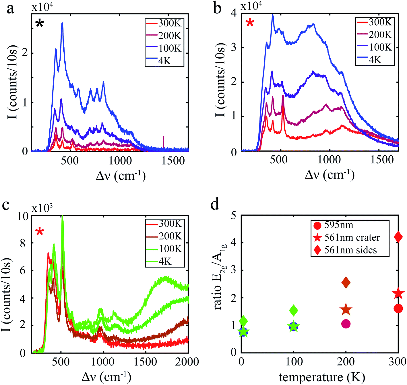 | ||
| Fig. 6 Temperature dependence of spectral features. (a and b) Spectra obtained as a function of temperature with a 595 nm excitation on the stair-like pyramid sides (black star in Fig. 4) and on the hollow pyramid middle (red star in Fig. 4), respectively. (c) Spectra obtained with a 561 nm excitation of the hollow pyramid middle as a function of temperature. The background visible at higher frequencies overlaps in wavelength with the background under the 595 nm spectra in Fig. 4b (see ESI Fig. S3†). (d) Temperature dependence of the intensity ratio of the first two Raman features, the fingerprint of WS2 material. The intensity ratio is presented for spectra upon 595 nm excitation (circles), spectra at the pyramid crater (stars) and pyramid sides (diamonds) upon 561 nm excitation. | ||
Fig. 6d presents the temperature dependence of the average intensity ratio of the first two Raman peaks (E2g/A1g). As shown in Fig. 4f, this ratio is not uniform over the pyramid, but is higher at the hollow pyramid middle than at the stair-like sides. This non-uniformity is most evident in the spectra obtained by 561 nm excitation (diamonds in Fig. 6d), as the A1g peak in the spectra from the pyramid sides almost completely disappears at room temperature (see ESI Fig. S5†). For a 595 nm excitation, at room temperature the first Raman peak (E2g, 2LA(M)) is 1.5× higher than the second Raman peak (A1g) and at 4 K this ratio is exactly inverted (circles in Fig. 6d). The peak ratio upon 561 nm excitation of spectra taken at the pyramid middle follow a similar temperature-dependent behaviour (stars in Fig. 6d).
The temperature-dependent intensity increase of TMDs Raman peaks has been reported previously for horizontal TMDs layers, and is attributed to an increase in phonon thermal population.31,32,35 The difference in intensity ratio between the E2g and A1g for the different excitation frequencies can be explained by the more resonant 595 nm laser exciting the Raman peaks differently than the out-of-resonance 561 nm laser.37,38 The strength of the exciton–phonon interaction, and therefore the resonance condition, is different for the in-plane E2g than the out-of-plane A1g Raman modes.38,52 This explains why the ratio E2g/A1g is higher for a 561 nm excitation, e.g., out-of-resonance with the excitonic transition, than for the resonant 595 nm excitation. The Raman intensity ratio also depends on the layer thickness of the material.27 However, the main difference in intensity ratio is reported between a monolayer and a bilayer, whereas we observe different relative Raman intensities between the few-layer pyramid crater and the thick pyramid edge. Moreover, the temperature-dependent behaviour of the Raman intensity also depends on the defect density in the sample.34 These factors are not mutually independent, e.g., the WS2 thickness influences the exciton–phonon interaction, the resonance of the excitation affects the influence of phonons and defects on the Raman intensity. The temperature dependence of the Raman peak intensities, excited with two different frequencies, is therefore an interplay between the phonon thermal population, the resonance conditions for the different phonon peaks and the defect density in the structure.
It is interesting to note in this context the intensity ratio of the first two Raman peaks on a WS2 monolayer, excited at 561 nm. This ratio is 1.4 at room temperature, much lower than both the intensity ratio at the hollow pyramid middle and at the stair-like sides, excited at 561 nm (see ESI Fig. S5†). Unexpectedly, this indicates a clear difference in structure and/or thickness between the WS2 monolayer and hollow pyramid. The large difference in intensity ratio on the hollow pyramid middle and the stair-like sides suggests a difference in atomic arrangement, pointing out that nanogeometrical differences induce spectral modifications.
III. Conclusions
We have studied the optical response of hollow WS2 pyramids, comparing them with WS2 monolayers grown on the same substrate. The optical response of these nanostructures is completely different, as hollow WS2 exhibit a strongly reduced photoluminescence with respect to WS2 monolayers. This enables us to study the rich variety of Raman peaks that the pyramids exhibit as a result of the resonant excitation. Following the hypothesis of a multiphonon excitation involving the longitudinal acoustic phonon LA(M), we are able to explain the origin of all 10–12 observed Raman resonances. In contrast with monolayers, the measured optical response of the pyramids is non-uniform in both intensity, intensity ratio between peaks, spectral shape and spectral position. We attribute the spectral differences between the hollow pyramid middle and the stair-like sides to differences in both nanogeometry and atomic arrangement. ADF-STEM measurements confirm variations in the atomic arrangement, where the level of disorder is more marked in the pyramid crater than on the sides. Next to a positional dependence, we measure the temperature dependent behaviour of the spectral response of the hollow WS2 pyramids. With decreasing temperature, the spectra change in intensity and shape. We see clear differences between spectra obtained with a resonant and out-of-resonance excitation laser. As the optical response of WS2 monolayers, exhibiting photoluminescence, is completely different, we therefore deduce to have fabricated a platform of structures with tunable optical properties. Both nanostructures offer exciting possibilities, with applications ranging from opto-electronics to non-linear optics.IV. Experimental section
The WS2 hollow pyramids are directly grown on a microchip using chemical vapour deposition (CVD) techniques. This microchip is composed of a silicon frame with nine windows over which a continuous silicon nitride (Si3N4) film is spanned. Preceding the CVD growth procedure,16 tungsten trioxide (WO3) is deposited onto the microchip. This deposition is achieved by dispersing 50 mg of WO3 in 1 mL of isopropanol, followed by a deposition by means of a pipette. The subsequent sulfurization process16 is carried out in a gradient tube furnace from Carbolite Gero. The microchip is placed in the middle zone and a crucible holding 400 mg of sulfur is placed upstream from it. The middle zone is heated to 750 °C, and kept at this reaction temperature for 1 hour after which the system is naturally cooled down to room temperature. Sulfurization is carried out under an argon flow of 150 sccm. The zone containing the sulfur is heated to 220 °C.The optical measurements are performed using a home-built spectroscopy set-up. We placed the sample in a Montana cryostation S100, using Attocube ANPxy101/RES piezo scanners to perform the presented raster scans. The small cross-coupling between the in-plane and out-of-plane piezo scanners causes a skewing between the x and y axis of the spectral-feature maps depicted in this work. Comparing the maps with the optical and SEM images of the pyramids, we can correlate the position of certain spectral features with the position on the pyramid. The cryostation is cooled down from room temperature to 200 K, 100 K and 4 K. The sample is illuminated through an 0.85NA Zeiss 100× objective. Two continuous wave lasers are used, one with a wavelength of 595 nm and a power of 1.6mW mm−2, and one with a wavelength of 561 nm and a power of 3.6 mW mm−2. To avoid the consequences of tight focussing on (circular) polarization, a 2 mm laser diameter is used, slightly underfilling the objective in the excitation path. This results in an excitation spot size of approximately 450 nm. A linear (vertical) polarization is used for the laser light. The sample emission is collected in reflection through the same objective as in excitation, and projected onto a CCD camera (Princeton Instruments ProEM 1024BX3) and spectrometer (Princeton Instruments SP2358) via a 4f lens system. The excitation light is filtered out using colour filters.
The transmission electron microscopy (TEM) measurements were carried out using an ARM200F Mono-JEOL microscope with Cs probed corrected. The microscope was operated at 200 kV both in TEM and STEM modes, with the monochromator on and a slit of 2 μm inserted. For the atomic resolution ADF-STEM measurements, an objective aperture of 30 μm and a camera length of 12 cm were used. The convergence semi-angle was 23 mrad.
Conflicts of interest
The authors declare no competing interests.Acknowledgements
The authors acknowledge funding from ERC Starting Grant “TESLA” No. 805021. The authors acknowledge dr Martin Caldarola and dr Filippo Alpeggiani for their help in the data analysis.References
- K. F. Mak, C. Lee, J. Hone, J. Shan and T. F. Heinz, Atomically thin mos2: a new direct-gap semiconductor, Phys. Rev. Lett., 2010, 105(13), 136805 CrossRef.
- T. Cao, G. Wang, W. Han, H. Ye, C. Zhu, J. Shi, Q. Niu, P. Tan, E. Wang, B. Liu and J. Feng, Valley-selective circular dichroism of monolayer molybdenum disulphide, Nat. Commun., 2012, 3, 887 CrossRef.
- X. Xu, Y. Wang, D. Xiao and T. F. Heinz, Spin and pseudospins in layered transition metal dichalcogenides, Nat. Phys., 2014, 10, 343 Search PubMed.
- B. Zhu, H. Zeng, J. Dai, Z. Gong and X. Cui, Anomalously robust valley polarization and valley coherence in bilayer ws2, Proc. Natl. Acad. Sci. U. S. A., 2014, 111(32), 11606–11611 CrossRef CAS.
- Y. J. Zhang, T. Oka, R. Suzuki, J. T. Ye and Y. Iwasa, Electrically switchable chiral light-emitting transistor, Science, 2014, 344(6185), 725–728 CrossRef CAS.
- Q. H. Wang, K. Kalantar-Zadeh, A. Kis, J. N. Coleman and M. S. Strano, Electronics and optoelectronics of two-dimensional transition metal dichalcogenides, Nat. Nanotechnol., 2012, 7, 699 CrossRef CAS.
- K. F. Mak, K. L. McGill, J. Park and P. L. McEuen, The valley hall effect in mos2 transistors, Science, 2014, 344(6191), 1489–1492 CrossRef CAS.
- J. R. Schaibley, H. Yu, G. Clark, P. Rivera, J. S. Ross, K. L. Seyler, Y. Wang and X. Xu, Valleytronics in 2d materials, Nat. Rev. Mater., 2016, 1, 16055 CrossRef CAS.
- S.-H. Gong, I. Komen, F. Alpeggiani and L. Kuipers, Nanoscale optical addressing of valley pseudospins through transverse optical spin, Nano Lett., 2020, 20(6), 4410–4415 CrossRef CAS PubMed . PMID: 32406694..
- J.-G. Song, J. Park, W. Lee, T. Choi, H. Jung, C. W. Lee, S.-H. Hwang, J. M. Myoung, J.-H. Jung, S.-H. Kim, C. Lansalot-Matras and H. Kim, Layer-controlled, wafer-scale, and conformal synthesis of tungsten disulfide nanosheets using atomic layer deposition, ACS Nano, 2013, 7(12), 11333–11340 CrossRef CAS PubMed.
- Y. Zhang, Y. Zhang, Q. Ji, J. Ju, H. Yuan, J. Shi, T. Gao, D. Ma, M. Liu, Y. Chen, X. Song, H. Y. Hwang, Y. Cui and Z. Liu, Controlled growth of high-quality monolayer ws2 layers on sapphire and imaging its grain boundary, ACS Nano, 2013, 7(10), 8963–8971 CrossRef CAS PubMed.
- C. Cong, J. Shang, X. Wu, B. Cao, N. Peimyoo, C. Qiu, L. Sun and Y. Ting, Synthesis and optical properties of large-area single-crystalline 2d semiconductor ws2 monolayer from chemical vapor deposition, Adv. Opt. Mater., 2014, 2(2), 131–136 CrossRef.
- C. M. Orofeo, S. Suzuki, Y. Sekine and H. Hibino, Scalable synthesis of layer-controlled ws2 and mos2 sheets by sulfurization of thin metal films, Appl. Phys. Lett., 2014, 105(8), 083112 CrossRef.
- A. Thangaraja, S. M. Shinde, G. Kalita and M. Tanemura, Effect of wo3 precursor and sulfurization process on ws2 crystals growth by atmospheric pressure cvd, Mater. Lett., 2015, 156, 156–160 CrossRef CAS.
- P. Liu, T. Luo, J. Xing, H. Xu, H. Hao, H. Liu and J. Dong, Large-area ws2 film with big single domains grown by chemical vapor deposition, Nanoscale Res. Lett., 2017, 12(1), 558 CrossRef PubMed.
- S. E. van Heijst, M. Mukai, E. Okunishi, H. Hashiguchi, L. I. Roest, L. Maduro, J. Rojo and S. Conesa-Boj, Illuminating the electronic properties of ws2 polytypism with electron microscopy, Ann. Phys., 2021, 2000499 CrossRef CAS.
- L. Zhang, K. Liu, A. B. Wong, J. Kim, X. Hong, C. Liu, T. Cao, S. G. Louie, F. Wang and P. Yang, Three-dimensional spirals of atomic layered mos2, Nano Lett., 2014, 14(11), 6418–6423 CrossRef CAS PubMed.
- P. V. Sarma, P. D. Patil, P. K. Barman, R. N. Kini and M. M. Shaijumon, Controllable growth of few-layer spiral ws2, RSC Adv., 2016, 6(1), 376–382 RSC.
- A. V. Agrawal, R. Kumar, G. Yang, J. Bao, M. Kumar and M. Kumar, Enhanced adsorption sites in monolayer mos2 pyramid structures for highly sensitive and fast hydrogen sensor, Int. J. Hydrogen Energy, 2020, 45(15), 9268–9277 CrossRef CAS.
- P. Cheng, Q. Zhou, X. Hu, S. Su, X. Wang, M. Jin, L. Shui, X. Gao, Y. Guan, R. Nözel, G. Zhou, Z. Zhang and J. Liu, Transparent glass with the growth of pyramid-type mos2 for highly efficient water disinfection under visible-light irradiation, ACS Appl. Mater. Interfaces, 2018, 10(28), 23444–23450 CrossRef CAS.
- Q. Zhou, S. Su, P. Cheng, X. Hu, M. Zeng, X. Gao, Z. Zhang and J.-M. Liu, Robust ferromagnetism in zigzag-edge rich mos2 pyramids, Nanoscale, 2018, 10(24), 11578–11584 RSC.
- J. Zheng, X. Yan, Z. Lu, H. Qiu, G. Xu, X. Zhou, P. Wang, X. Pan, K. Liu and L. Jiao, High-mobility multilayered mos2 flakes with low contact resistance grown by chemical vapor deposition, Adv. Mater., 2017, 29(13), 1604540 CrossRef.
- L. Chen, B. Liu, A. N. Abbas, Y. Ma, X. Fang, Y. Liu and C. Zhou, Screw-dislocation-driven growth of two-dimensional few-layer and pyramid-like wse2 by sulfur-assisted chemical vapor deposition, ACS Nano, 2014, 8(11), 11543–11551 CrossRef CAS.
- X. Fan, Y. Jiang, X. Zhuang, H. Liu, T. Xu, W. Zheng, P. Fan, H. Li, X. Wu, X. Zhu, Q. Zhang, H. Zhou, W. Hu, X. Wang, L. Sun, X. Duan and A. Pan, Broken symmetry induced strong nonlinear optical effects in spiral ws2 nanosheets, ACS Nano, 2017, 11(5), 4892–4898 CrossRef CAS PubMed.
- X. Lin, Y. Liu, K. Wang, W. Cong, W. Zhang, Y. Yan, Y. J. Li, J. Yao and Y. S. Zhao, Two-dimensional pyramid-like ws2 layered structures for highly efficient edge second-harmonic generation, ACS Nano, 2018, 12(1), 689–696 CrossRef CAS PubMed.
- C. Lee, H. Yan, L. E. Brus, T. F. Heinz, J. Hone and S. Ryu, Anomalous lattice vibrations of single- and few-layer mos2, ACS Nano, 2010, 4(5), 2695–2700 CrossRef CAS PubMed.
- W. Zhao, Z. Ghorannevis, K. Kumar Amara, J. R. Pang, M. Toh, X. Zhang, C. Kloc, P. H. Tan and G. Eda, Lattice dynamics in mono- and few-layer sheets of ws2 and wse2, Nanoscale, 2013, 5, 9677–9683 RSC.
- A. Berkdemir, H. R. Gutiérrez, A. R. Botello-Méndez, N. Perea-López, A. L. Elías, C.-I. Chia, B. Wang, V. H. Crespi, F. López-Urías, J.-C. Charlier, H. Terrones and M. Terrones, Identification of individual and few layers of ws2 using Raman spectroscopy, Sci. Rep., 2013, 3(1), 1755 CrossRef.
- A. A. Mitioglu, P. Plochocka, G. Deligeorgis, S. Anghel, L. Kulyuk and D. K. Maude, Second-order resonant Raman scattering in single-layer tungsten disulfide ws2, Phys. Rev. B: Condens. Matter Mater. Phys., 2014, 89(24), 245442 CrossRef.
- M. R. Molas, K. Nogajewski, M. Potemski and B. Adam, Raman scattering excitation spectroscopy of monolayer ws2, Sci. Rep., 2017, 7(28698679), 5036 CrossRef.
- N. Peimyoo, J. Shang, W. Yang, Y. Wang, C. Cong and Y. Ting, Thermal conductivity determination of suspended mono- and bilayer ws2 by Raman spectroscopy, Nano Res., 2015, 8(4), 1210–1221 CrossRef CAS.
- A. P. S. Gaur, S. Sahoo, J. F. Scott and R. S. Katiyar, Electron-phonon interaction and double-resonance Raman studies in monolayer ws2, J. Phys. Chem. C, 2015, 119(9), 5146–5151 CrossRef CAS.
- L. Xue, J. Li, K. Wang, X. Wang, S. Wang, X. Chu, M. Xu, X. Fang, Z. Wei, Y. Zhai and B. Zou, Pressure and temperature-dependent Raman spectra of mos2 film, Appl. Phys. Lett., 2016, 109(24), 242101 CrossRef.
- J. Li, W. Su, F. Chen, L. Fu, S. Ding, K. Song, X. Huang and L. Zhang, Atypical defect-mediated photoluminescence and resonance Raman spectroscopy of monolayer ws2, J. Phys. Chem. C, 2019, 123(6), 3900–3907 CrossRef CAS.
- J.-He Fan, P. Gao, A.-M. Zhang, B.-R. Zhu, H.-L. Zeng, X.-D. Cui, R. He and Q.-M. Zhang, Resonance Raman scattering in bulk 2h-mx2 (m-mo,w, x-s,se) and monolayer mos2, J. Appl. Phys., 2014, 115(5), 053527 CrossRef.
- S.-Y. Chen, C. Zheng, M. S. Fuhrer and J. Yan., Helicity-resolved Raman scattering of mos2, mose2, ws2, and wse2 atomic layers, Nano Lett., 2015, 15(4), 2526–2532 CrossRef CAS.
- B. R. Carvalho, L. M. Malard, J. M. Alves, C. Fantini and M. A. Pimenta, Symmetry-dependent exciton-phonon coupling in 2d and bulk mos2 observed by resonance Raman scattering, Phys. Rev. Lett., 2015, 114, 136403 CrossRef PubMed.
- E. del Corro, A. Botello-Méndez, Y. Gillet, A. L. Elias, H. Terrones, S. Feng, C. Fantini, D. Rhodes, N. Pradhan, L. Balicas, X. Gonze, J.-C. Charlier, M. Terrones and M. A. Pimenta, Atypical exciton–phonon interactions in ws2 and wse2 monolayers revealed by resonance Raman spectroscopy, Nano Lett., 2016, 16(4), 2363–2368 CrossRef CAS . PMID: 26998817..
- L. P. McDonnell, C.-C. Huang, Q. Cui, D. W. Hewak and D. C. Smith, Probing excitons, trions, and dark excitons in monolayer ws2 using resonance Raman spectroscopy, Nano Lett., 2018, 18(2), 1428–1434 CrossRef CAS PubMed.
- J. E. Zucker, A. Pinczuk, D. S. Chemla, A. Gossard and W. Wiegmann, Raman scattering resonant with quasi-two-dimensional excitons in semiconductor quantum wells, Phys. Rev. Lett., 1983, 51, 1293–1296 CrossRef CAS.
- K. Gołasa, M. Grzeszczyk, P. Leszczyński, C. Faugeras, A. A. L. Nicolet, A. Wysmołek, M. Potemski and A. Babiński, Multiphonon resonant Raman scattering in mos2, Appl. Phys. Lett., 2014, 104(9), 092106 CrossRef.
- R. Yang, S. Feng, X. Lei, X. Mao, A. Nie, B. Wang, K. Luo, J. Xiang, F. Wen, C. Mu, Z. Zhao, B. Xu, H. Zeng, Y. Tian and Z. Liu, Effect of layer and stacking sequence in simultaneously grown 2h and 3r ws2 atomic layers, Nanotechnology, 2019, 30(34), 345203 CrossRef CAS.
- L. Du, Q. Zhang, T. Zhang, Z. Jia, J. Liang, G.-B. Liu, R. Yang, D. Shi, J. Xiang, K. Liu, Z. Sun, Y. Yao, Q. Zhang and G. Zhang, Robust circular polarization of indirect q-k transitions in bilayer 3r – Ws2, Phys. Rev. B, 2019, 100, 161404 CrossRef CAS.
- M. Thripuranthaka, R. V. Kashid, C. S. Rout and D. J. Late, Temperature dependent Raman spectroscopy of chemically derived few layer mos2 and ws2 nanosheets, Appl. Phys. Lett., 2014, 104(8), 081911 CrossRef.
- J. H. Parker, D. W. Feldman and M. Ashkin, Raman scattering by silicon and germanium, Phys. Rev., 1967, 155(3), 712–714 CrossRef CAS.
- K. Uchinokura, T. Sekine and E. Matsuura, Raman scattering by silicon, Solid State Commun., 1972, 11(1), 47–49 CrossRef CAS.
- B. A. Weinstein and M. Cardona, Two-phonon Raman spectra of si and gap, Solid State Commun., 1972, 10(10), 961–965 CrossRef CAS.
- S. Mignuzzi, A. J. Pollard, N. Bonini, B. Brennan, I. S. Gilmore, M. A. Pimenta, D. Richards and D. Roy, Effect of disorder on Raman scattering of single-layer Mos2, Phys. Rev. B: Condens. Matter Mater. Phys., 2015, 91(19), 195411 CrossRef.
- W. M. Parkin, A. Balan, L. Liang, P. M. Das, M. Lamparski, C. H. Naylor, J. A. Rodríguez-Manzo, A. T. Charlie Johnson, V. Meunier and M. Drndić, Raman shifts in electron-irradiated monolayer mos2, ACS Nano, 2016, 10(4), 4134–4142 CrossRef CAS PubMed.
- C. Rice, R. J. Young, R. Zan, U. Bangert, D. Wolverson, T. Georgiou, R. Jalil and K. S. Novoselov, Raman-scattering measurements and first-principles calculations of strain-induced phonon shifts in monolayer mos2, Phys. Rev. B: Condens. Matter Mater. Phys., 2013, 87(8), 081307 CrossRef.
- L. Yang, X. Cui, J. Zhang, K. Wang, M. Shen, S. Zeng, S. A. Dayeh, F. Liang and B. Xiang, Lattice strain effects on the optical properties of mos2 nanosheets, Sci. Rep., 2014, 4(1), 5649 CrossRef CAS PubMed.
- D. Mastrippolito, S. Palleschi, G. D'Olimpio, A. Politano, M. Nardone, P. Benassi and L. Ottaviano, Exciton-phonon coupling and power dependent room temperature photoluminescence of sulphur vacancy doped mos2 via controlled thermal annealing, Nanoscale, 2020, 12(36), 18899–18907 RSC.
Footnote |
| † Electronic supplementary information (ESI) available: SEM and ADF-STEM images for more information about the morphology and crystal structure of the hollow pyramids. Discussion about the origin of the background in the spectral response of the pyramids. Comparison of the spectral features (Raman intensity, peak ratio and peak position) of the hollow WS2 pyramid at different temperatures, and between the WS2 monolayer, hollow pyramid and full pyramid. Overview of the measured Raman features. See DOI: 10.1039/d1na00531f |
| This journal is © The Royal Society of Chemistry 2021 |